

Page 1
MH88612C
Subscriber Line Interface Circuit
Preliminary Information
Features
• Input impe danc e 200Ω + 560Ω // 0.1µF
• Transformerless 2 -wire to 4- wire con versi on
• Battery and ringing feed to line
• Off-hook and dial pulse detection
• Ring gr oun d over-curren t protection
• Adjustable consta nt curre nt fee d
• Relay drive outp ut
• Power VBat De nial
• Wide Operating Range
• Programmable Receive Gain
Applications
Line interface for:
• PABX
• Intercom s
• Key Telephone Sys tems
• Control Syst ems
ISSUE 4 April 1995
Ordering Information
MH88612C 20 Pin SIL Package
0°C to 70°C
Descript io n
The SLIC provides a complete interface between a
switching system and subscriber loop. Functions
provided include battery feed and ringing feed to the
subscriber line, 2-Wire to 4-Wire hybrid interfacing,
constant current feed and dial pulse detection. The
device is fabricated using thick film hybrid
technology in a 20-pin single in-line package.
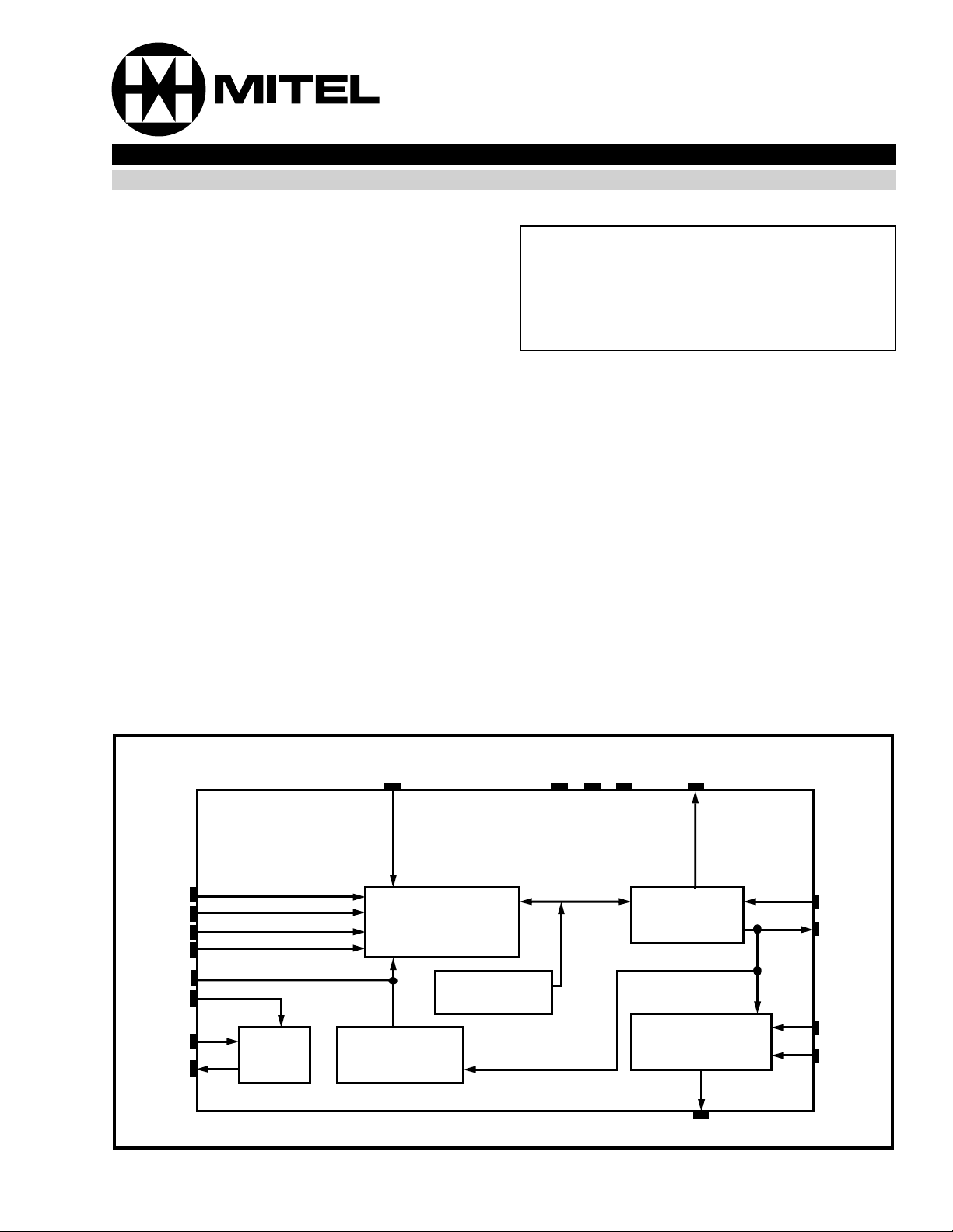
TF
TIP
RING
RF
RV
VRLY
RC
RD
Relay
Drive
Circuit
VBat
Current & Voltage
Sensing
Over Current
Protection
Constant
Current
Feed
FIgure 1 - Functional Block Diagram
VDD VEE GNDA
GS
2-Wire to
4-Wire
Conversion
Loop
Supervision
SHK
VR
VX
VRef
CAP
2-113
Page 2
MH88612C Preliminary Information
IC
TF
IC
VR
VRef
VEE
GNDA
GS
VX
TIP
RING
RF
VDD
RC
RD
RV
VRLY
IC
VBat
CAP
SH K
0
1
2
3
4
5
6
7
8
9
10
11
12
13
14
15
16
17
18
19
20
Figure 2 - Pin Connections
Pin Description
Pin # Name Description
0ICInternal Connection. No pin fitted in this position.
1TFTip Feed. Connects to external diode to LPGND for protection.
2ICInternal Connection. No pin fitted in this position.
3VRVoice Receive (input) is the 4 wire analog sign al to the SLIC.
4VRefVoltage Reference to set the constant current feed to the subscriber line. Constant current
feed can be adjusted by the input voltage on the VRef. This pin can also be grounded for
normal 21mA loop current.
5VEE Negative Power Supply voltage. (-5V).
6GNDAAnalo g Ground. (0V)
7GS
Gain setting (Input). A logic low at this input adds an additional -0.5dB gain in the receive
direction. This gain is in additio n to the gai n set by the Codec. A high adds 0dB gain.
8VXVoice Transmit (Output) is the 4-wire analog signal from the SLIC.
9 TIP Connects to the “Tip” lead of the telephone line.
10 RING Connects to the “Ring” lead of the telephone line.
11 RF Ring Feed (Input). is connected via the ring relay to either negative battery feed voltage,
(RV), or ringing voltage input.
12 VDD Positive Power Supply Voltage. (+5V)
13 RC Relay Con trol (Input). Active high will appl y ringing to th e line.
14 RD Outpu t Drive Sources current when RC is at a logic high.
15 RV Ring Feed Voltage connects to pin 11 (RF) through a normally closed relay contact.
16 VRLY Relay voltage Supply. (+5V)
17 IC Internal Connection. No pin fitted in this position.
18 VBat Negative Battery Feed Supply Voltage. (-48V)
19 CAP Co n nects externa l capacitor to ground for ring trip.
20 SHK Switch Hoo k Detect (Outp ut). Active high.
2-114
Page 3

Preliminary Information MH88612C
Functional Description
The SLIC performs a transformerless 2-wire to
4-wire conversion of the analog signal. The 2-wire
circuit is the balanced line going to the subscriber
loop, while the 4-wire circuit is the audio signal going
to and from devices such as the voice codec or
switching circuit. The SLIC also provides a switch
hook (SHK) status output which goes high when the
telephone is set off-hook.
Constant Current Feed
The SLIC employs a complex feedback circuit to
supply a constant feed current to the line. This is
done by sensing the sum of the voltages across the
internal feed resistors and comparing it to an input
reference v o lt ag e ( V
feed current. If V
the constant current is set at 21mA. For a constant
current setting between 18mA and 30mA, V
be set between -8.75 Vdc and -6.35 Vdc. The
relationship is detailed in the formula below:
) that determines the constant
Ref
(pin 4) is externally grounded,
Ref
Ref
can
For applications requiring dial pulse detection the
capacitor connection to ground should be controlled
so that the capacitor is only connected during
ringing.
During off-hook conditions (closed loop), the
capacitor should be switched out. This can be
performed using a transistor, relay to system drive
output of a codec. Applying GNDA to Ring Trip Filter
Control pin will switch in the filter, whilst removing
GNDA, (with the switch in a tristate condition), will
switch out the filter.
For applications using DTMF signalling, the
capacitor can be permanently connected to ground.
Once an off-hook condition has been detected a
logic low on the Relay Control (RC) input deactivates
the relay (K1) to disconnect the ringing voltage from
pin 11 (RF)and reconnect to pin 15 (RV). At that time
the SLIC will revert to constant current feed
operation.
Current Limit
I
Loop
= [-2.6(V
) + 21.5] mA +2mA
Ref
Switch Ho ok Det ecti on
When the DC current exceeds an internal threshold
level, the switch hook (SHK) will go high. If the loop
resistance is so high that V
can no longer supply
Bat
the required amount of loop current as determined
by constant current supply circuit, the output of the
switch hook (SHK) will go low to indicate that the
loop resistance is too high and the line is on hook.
Ringing And Ring Trip Detection
In Figure 3 a ringing signal (e.g. 90 Vrms
superimposed on -48 VDC) is applied to the line by
disconnecting pin 15 (RV) from pin 11 (FR), and
connecting the ringing voltage at pin 11 (RF) by use
of the relay K1.
The SLIC can detect an off-hook condition during
ringing but there is a large AC component which
must be filtered out to give a true off-hook condition
at SHK.
The Tip or Ring may accidentally short to ground. In
such a case, current will only flow through the feed
resistor. This high current will be sensed and
reduced by the current limit circuit to a lower value to
protect the internal circuitry.
Receive G ain
The MH88612C Receive Gain (VR to 2-wire) can be
adjustable by -0.5dB if GS
0dB if GS
is taken logic high. When the MH88612C
issued with an off hybrid MT896x codec the Receive
Gain can be set to either -3.5dB or -7dB by writing to
control Register A of Codec and programming GS
appropriately.
is taken logic low or by
A 1µF capacitor connected from pin 19 (CAP) to
ground will provide adequate attenuation when
ringing is applied.
2-115
Page 4

MH88612C Preliminary Information
Applications
Component L ist
R1 = 1/4 W, +
10% 200Ω
R2, = 1/4W, ±5%, 470KΩ
C1 = Cap. Elec., 1.0µF, +
10%, 25V
D1,D2 = Diode R e ct., 200V, 1A, IN 4 00 3
K1 = Relay E/M, 5 or 6V, 1 form C
Decoupling capacitors (Cap. Cer 0.1µF, 50% + 20%) should be added to V
and V
RLY
.
Options RV1, RV2= 160 Vrms, 250V 10J
D4
D1
D2
D3
VBat
15
11
MH88612C
RF
RV
TF
1
VR
VX
3
8
90 VRMS
SUPERIMPOSED
ON -48VDC
R1
K1
, VEE, V
DD
Bat
, V
Ref
RV1
RV2
+5V
K1
VBat
10
13
16
14
9
TIP
RING
RC
VRLY
RD
18
-48V
12
VDDVBat
+5V
VEE
5
-5V
VRef
SHK
GS
CAP
GNDA
6
4
20
7
19
C1
-
+
R2
Ring Trip
Filter
Control
2-116
Figure 3 - Application Circuit
Page 5

Preliminary Information MH88612C
Absolute Maximum Ratings*
Parameter Symbol Min Max Units
1 DC Supply Voltage V
2 Storage Temperature T
3 Package Power Dissipation P
* Excee di ng these values ma y cause perm anen t damage . Function al ope rati on under the se conditi ons is not impl ied.
V
V
DD
EE
Bat
STG
D
-0.3
+0.3
0.3
+15
-15
-60
-40 100 °C
2w
Recommended Operating Conditions
Parameter Sym Min Typ* Max Units Commen ts
1 Operating Supply Voltage V
2 Operating Temperature T
* Typical figures are at 25°C and are for desi gn aid only.
DD
V
EE
V
Ref
V
Bat
V
RLY
O
4.75 5.0 5.25 V
-4.75 -5.0 -5.25 V
0 V Adjustable
-27 -48 -60 V
5V
070°C
DC Electrical Characteristics† - Voltages are with respect to GNDA unless otherwise stated.
Characteristics Sym Min Typ* Max Units Test Conditions
1 Supply Current
V
DD
V
EE
VBat
2 Power Consumption P
3 Constant Current Line Feed I
4 Adjustable Loop Current Rang e I
5 Operating Loop Resistance R
I
DD
I
EE
I
BAT
Loop
Loop
Loop
C
6 Ring Ground Over-Current
protection
7 Off-Hook Detect
Output Low Current (On-hook)
Output High Current (Off-hook)
V
OL
V
OH
8 Off- Hook Detect
Output Low Current (on-hook)
Input High Current. (activation)
I
I
OL
OH
9 RC Control Input
Input Low Volt. (no activation)
Input High Volt. (activation)
V
IL
V
IH
10 RC control Input
Input Low Current (no
I
IL
activation)
Input high current (activation)
† DC Electrical Characteristics are over recommended operating supply voltages.
* Typical figures are at 25°C with nominal +/-5V supplies and are for design aid only.
I
IH
0.8
0.5
0.0
18 21 24 m A V
5
3
2
210
1410
12
10
2.5
mA
mA
mA
Idle State
mWmWStandby
Active
= GNDA,
Ref
= -48V
V
Bat
18 30 mA Adjustable with Ext.
V
input, V
Ref
1850 Ω V
= -48V @ I
Bat
18mA, R
telephone set
40 m A
Active high logic
0.0
2.7
0.4
5.25
8
-400
V
V
mA
µA
Active high logic
0.7 V
2.0
-50
50
V
µA
µA
Bat
includes
Loop
V
V
V
= -48V
=
Loop
2-117
Page 6

MH88612C Preliminary Information
AC Electrical Characteristics
Characteristics Sym Min Typ* Max Units Test Conditi ons
1 Ringing Voltage V
RING
40 90
25
V
rms
Hz
Superimposed on
V
2 Ringer Equivalence Numbe r REN 3
3 Ring Trip Detect time 100 ms
4 Input AC Impedance 2-wire
Z
in
719 Ω @1020Hz
(1)
5 Input Impedance at V
6 Output Impedance at V
7 Gain 2-wire to V
X
R
X
100 kΩ
10 Ω
0
dB
Input 3 dBm, 1kHz across
Tip and Ring,
Gain relative to Gain @ 1kHz -0.5
-0.22
0.1
0.1
dB
dB
300Hz & 3k4Hz
600Hz & 2k4Hz
Z
8 Gain V
Gain relative to Gain @ 1kHz
with GS
to 2-wire
R
@ logic high
-0.6
-0.5
0.22
Input 1.0V
0
-0.4
0.1
0.1
dB
dB
dB
dB
with GS @ at logic high
with GS
300Hz & 3k4Hz
600Hz & 2k4Hz
Z
9 2-wire Return Loss over
300-3400Hz
20 30 dB Inp ut 0.5 V
and Ring, Z
network. See Note (1).
10 Transhybrid Loss over
300-3400 Hz
THL 20 35 dB Input 0.5V V
complex network. See
Note (1).
11 Longitudinal to Metallic
46 55 dB Inp ut 1 V
Balance over 300-3400 Hz
12 Total Harmonic Distortion
at V
THD
X
0.1
1.0
%
Input 3dBm, 1 kHz
across Tip and Ring,
Inp ut 1.0 V
at Tip and Ring
13 Common Mode Rejection
CMRR 40 50 dB I np ut 1 V
0.1
1.0
%
Ratio
2-wire to V
14 Idl e channel Noise (at V
15 Power supply rejection ratio
X
)
X
(at T & R)
Nc 14
-76
12
-78
dBrnC
dBrnp
dBrnC
dBrnp
C- Message
psophemetric
C- Message
psophometric
PSRR
V
DD
V
EE
V
Bat
20
20
20
30
30
30
dB
dB
dB
1 V
V
Vx and across Tip and
Ring
* Typical figure are at 25°C and are for design aid only: not guaranteed and not subject to production testing.
Note (1): Zin = 200 + 560Ω //0.1µF
=-48V
Bat
See Note (1).
Load
rms
@ at logic low
, See Note (1).
Load
rms ,
Load
rms
rms
, 1KHz
rms
ripple, 1 k H z o n
PP
DD/VEE//VBat
, 1kHz @ V
acro s s Tip
= complex
rms, ZLoad
=
1kHz at V
,measure at
R
R
2-118
Page 7

Preliminary Information MH88612C
Side View
0.010 +
(0.25 +
Notes:
1) N ot to scal e
2)Dimensi ons in inches).
3) (Dimensions in millimetres).
*Dimensio ns to centre of pin &
tolerance non ac cumulati ve.
0.002
0.05)
0.080 Max
(2.0 Max)
0.27 Max
(6.9 Max)
0.6 Max
(15.3 Max)
0.025 Max
1
*
0.02
0.15 +
0.5)
(3.81 +
Figure 4 - Mechanical Data
2.13 Max
(54.34 Max)
0.020 typ
0.100 +
(2.54 +
20
0.05 + 0.02
0.5)
(1.3 +
*
0.010
0.26)
*
0.180 +
(4.6 +
0.02
0.5)
2-119
Page 8

MH88612C Preliminary Information
Notes:
2-120
 Loading...