

Page 1
MH88524
Dual 2-4 Wire Circuit
Preliminary Information
Features
• Full duple x operat ion
• Two complete circuits per package
• Transformerless 2-4 W ire (4 -2 Wire) conversi on
5V operation
•+
• Wide bandwidth (50kHz)
• Small Package Size
Applications
4-2 Wire and 2-4 Wire conversion for:
• MH88630/ 631, MH88 632, MH88 50 0 & MT8 840
• PBX
• Key Telephone Sy stem
• Channel b ank
•Voice Mail
• Terminal Equipm ent
• Digital Loop Carrier
• Modem
• Intercom
ISSUE 4 April 1995
Ordering Information
MH88524 10 Pin SIL Pa ckag e
0°C to 70°C
Descript io n
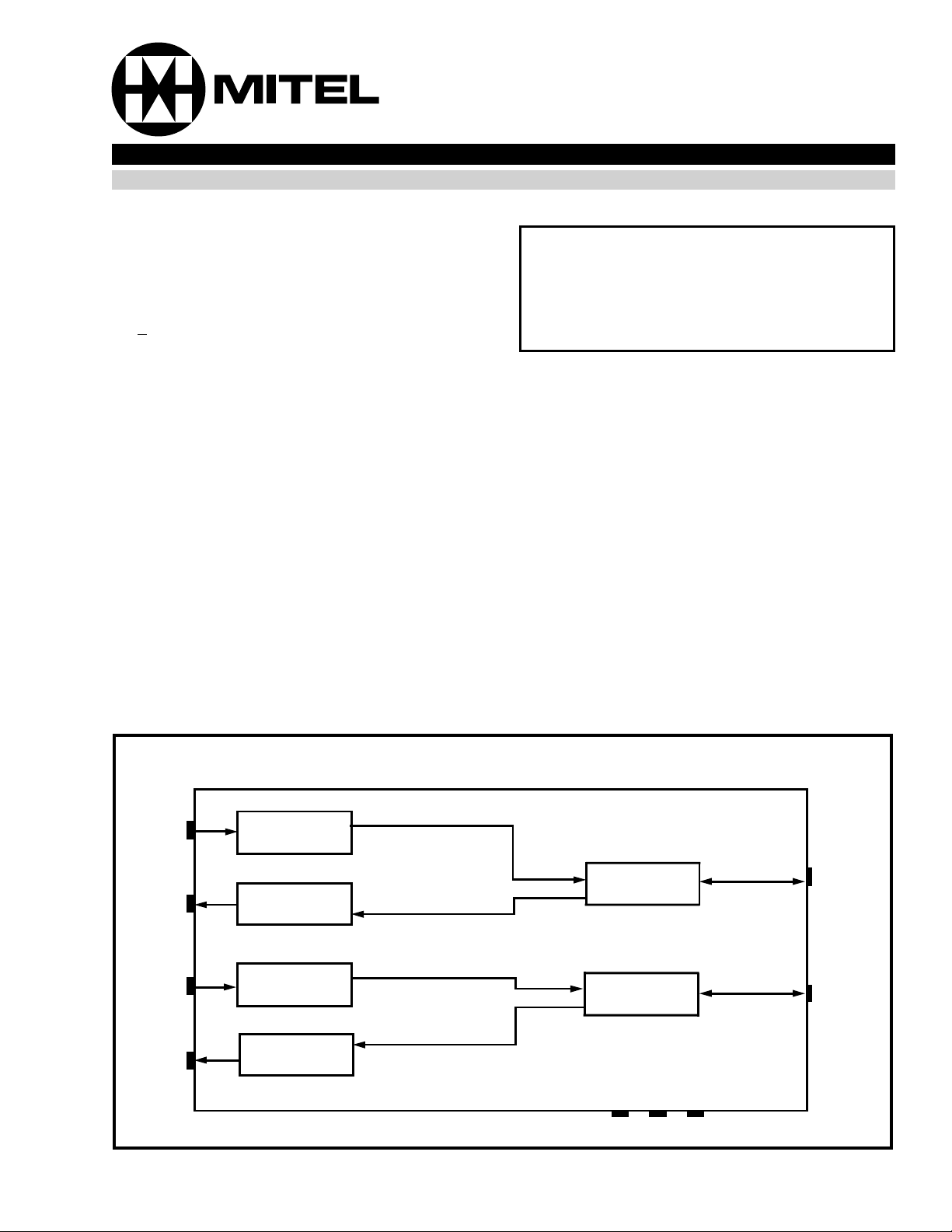
The Mitel MH88524 (Dual 2-4 wire Circuit) provides
two independent interfaces between4-Wire devices
such as the MH 8 86 3 1 CO IC (Central Offi ce In te rfa c e
CIrcuit) and a speech switch such as the MT8814
(Analog Switch Array), requiring only a single
bidirectional switch per crosspoint. The MH88524
can accommodate two full duplex audio links. The
device is fabricated as a thick film hybrid which
incorporates various technologies for optimum circuit
design and very high reliability.
RX1
TX1
RX2
TX2
Receive Gain
Circuit1
Transmit Gai n
Circuit 1
Receive Gain
Circuit 2
Transmit Gain
Circuit 2
VDD VEE AGND
Figure 1 - Functiona l Block Dia gram
2-4 Wire
Circuit 1
2-4 Wire
Circuit 2
JUN1
JUN2
2-73
Page 2
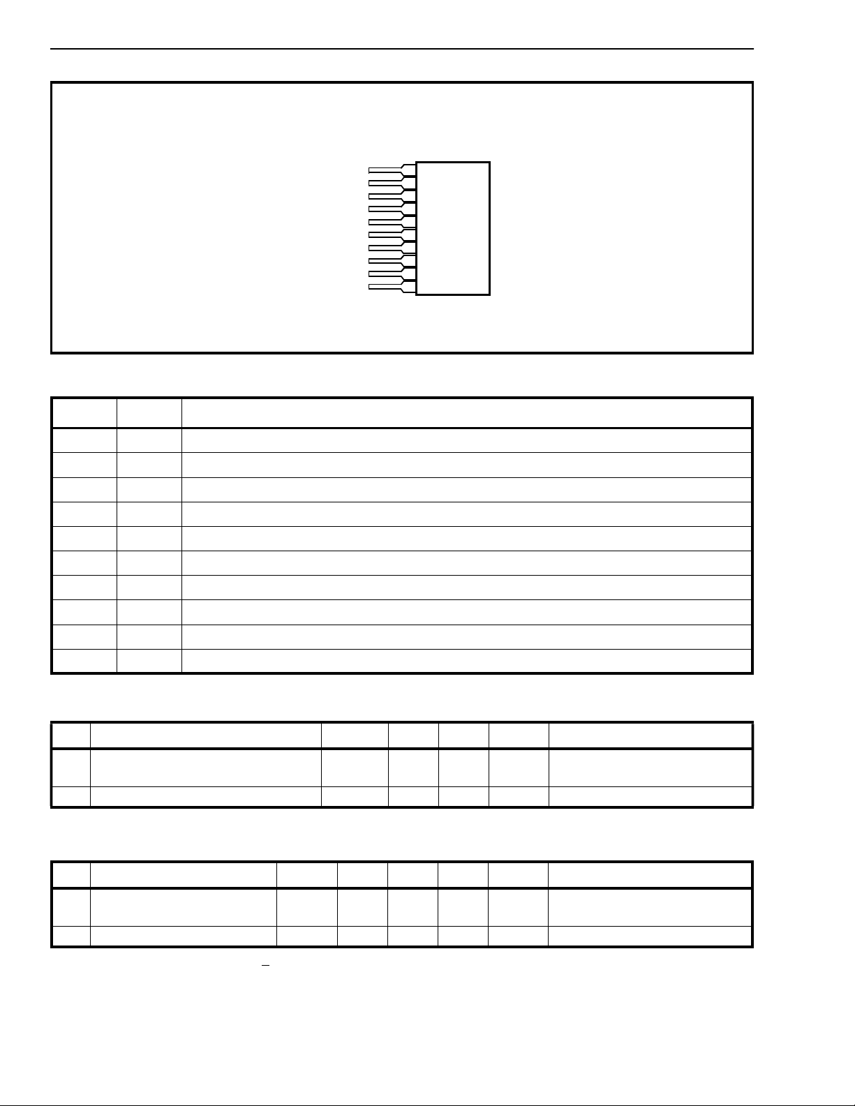
MH88524 Preliminary Information
RX1
JUN1
TX1
VDD
AGND
VEE
IC
TX2
JUN2
RX2
1
2
3
4
5
6
7
8
9
10
Figure 2 - Pin Connections
Pin Description
Pin # Name Description
1RX1Receive 1 (Input). 4-Wire ground (AGND) referenced audio out put .
2 JUN1 Junctor 1 (Transmit and Receive). Ground referenced transmit and receive speech path.
3TX1Transmit 1. 4-Wire ground (AGND) referenced audio output.
4VDDPositive Supply Voltage. Typically +5V.
5AGNDAnalog Gr ou nd. 2-Wire and 4-Wire ground . Normally connecte d to System Ground.
6 VEE Negative Su pp ly Voltage. Typically -5V.
7ICInternal Connection. This pin is internally connected.
8TX2Transmit 2 (Output). 4-Wire gro und AGND) referenced audi o outp ut.
9 JUN2 Junctor 2 (Transmit and Receive). Ground referenced transmit and receive speech path.
10 RX2 Receive 2 (Input). 4-Wire ground (AGND) refere nced audio output .
Absolute Maximum Ratings*
Parameter Sym Min Max Un its Comment s
1 DC Supply Voltage V
2 Storage Temperature T
* Exceeding these values ma y cause perm anen t dama ge. Functi onal operati on und er these cond ition s is not implied.
DD
V
EE
S
-0.3
+0.315-15
-55 125 °C
V
With respect LG ND
V
Recommended Operating Conditions
Parameter Sym T yp* Min Max Units Comments
1 DC Supply Voltage V
2 Operating Temperature T
* Typical figures are at 25°C with nominal +5V supplies and are for design aid only.
DD
V
EE
OP
5.0
-5.0
4.75
-4.7510-10
V
V
070°C
2-74
Page 3

Preliminary Information MH88524
DC Electrical Characteristics
‡
Characteristics Sym Min Typ* Max Uni ts Test Conditions
1 Supply Current I
DD
P
EE
4
4
mA VDD = +5.0
2 Power Dissipation PC 40 mW V
‡ DC Electrical Characteristics are over recommended operating conditions unless otherwise stated.
* Typical figures are at 25°C with nominal +5V supplies and are for design aid only.
AC Electrical Interdependence Characteristics
‡
Characteristics Sym Min Typ* Ma x Units Test Conditions
1 Cross, Circuit 1 or 2
JUN1 to JUN2
JUN1 to TX2
RX1 to JUN2
RX1 to TX2
JUN1 to JUN2
JUN1 to TX2
RX1 to JUN2
RX1 to TX2
80
80
80
80
60
60
60
60
dB
dB
dB
dB
dB
dB
dB
dB
2 Crosstalk, Circuit 1 or 2
= 5.0
V
EE
= +5.0
DD
= 5.0
V
EE
Input 1.0V
200Hz-3400Hz
200Hz-50kHz
Input 1.0V
JUN1 to JUN2
JUN1 to TX2
RX1 to JUN2
RX1 to TX2
JUN1 to JUN2
JUN1 to TX2
RX1 to JUN2
RX1 to TX2
‡ AC Electrical Characteristics are over recommended operating conditions unless otherwise stated.
* Typical figures are at 25°C with nominal +5V supplies and are for design aid only.
80
80
80
80
60
60
60
60
dB
dB
dB
dB
dB
dB
dB
dB
200Hz-3400Hz
200Hz-50kHz
2-75
Page 4

MH88524 Preliminary Information
AC Electrical Characteristics
‡
Characteristics Sym Min Typ* Max Units Test Conditions
1 Ret urn Loss at junctor①
(Ref. = 604Ω )
46
40
dB
dB
200-3400Hz
200-50kHz
2 Impedance at Junctor 604 Ω
3 Transhybrid Loss②
(Junctor - 754Ω)
4 Transhybrid Loss ③
(Frequency = 1kHz)
5 Transhybrid Loss
(Frequency = 50kHz)
42
36
18
21
15
18
dB
dB
dB
dB
dB
dB
200-3400Hz
200-50kHz
Junctor = 600Ω
Junctor = 900Ω
Junctor = 600Ω
Junctor = 900Ω
6 Inp ut Impedance at RX 10k Ω
7 Output Impedance at TX 5 Ω
8 Gain RX to Junctor
9 Frequen cy Response Gain
(relative to gain at 1kHz)
10 Gain junctor to TX AJT 0.99
11 Frequen cy Response Gain
relative to gain at 1kHz
12 Signal Output Overload Level
at TX
at Junctor
13 Total Harmonic Distortion
RX to Junctor
Junctor to TX
RX to Junctor
Junctor to TX
14 Idle Channel Noise
at TX
at Junctor
15 Power Supply Rejection Ratio
ARJ
THD
Nc
PSRR
0.99
-0.1
-0.1
-0.1
-0.1
-0.1
-0.1
6.0
6.0
1.00
0.0
1.01
0.1
0.1
1.0
1.0001.01
0.1
0.1
0.1
0.4
0.4
1.0
1.0
2
2
V/V
dBV
dB
dB
V/V
dBV
dB
dB
dBm
dBm
%
%
%
%
dBrnC
dBrnC
Input 0.5V 1kHz
200-3400Hz
200-50kHz
Input 0.5V 1kHz
200-3400Hz
200Hz-50kHz
%THD<5%
Reference: 6 00 Ω
Reference: 7 54 Ω
Input 0.5V 1kHz
200-3400Hz
200-3400Hz
200-50kHz
200-50kHz
Reference: 6 00 Ω
Referenc e 754Ω
Ripple 0.1V 1kHz
at TX and Junctor
V
DD
V
EE
* Typical figure are at 25°C with nominal +5V supplie s and are for desig n aid only.
‡ AC Electrical Characteristics are over recommended operating conditions unless otherwise stated.
Both of the 2-4 Wire circuits are tested. TX, RX and Junctor actual ly refer to TX1, RX1 and JUN1; and TX2, RX2 and JUN2.
All of the above test conditions use 754Ω connected between Junctor and AGND, unless otherwise stated.
All the above test conditions use 200Hz to 3400Hz unless otherwise stated.
Notes:
① RX is connected to AGND, see Figure 3.
② See Figure 5.
③ See Figure 4.
40
40
dB
dB
2-76
Page 5

Preliminary Information MH88524
Functional Description
The MH88524 is a Dual 2-4 Wire Circuit used to
interface between ground reference 2-Wire circuitry
and ground referenced 4-Wire circuitry. The device
can accommodate two full duplex audio links.
Hybrid
The 2-4 Wire hybrid circuit separates the ground
reference full duplex s ignal at JUNi (where i=1 or 2)
of the switched line into receive and transmit ground
referenced signals the RXi (Receive) and TXi
(Transmit). The hybrid also prevents the input signal
at RXi from appearing at TXi. The degree to which
the hybrid minimises the contribution to the RXi
signal at the TXi output is specified as transhybrid
loss. For maximising transhybrid loss, see the
Transhybrid Loss section.
The 4-Wire side c an be interfaces to a COIC such as
the MH88631 for use in analog voice switched
systems; or a filter/codec, such as the Mite l MT896X,
for use in digital voice switched systems.
Figure 6, shows, illustrates a typical connection
between an Interface Circuit (MH88631) and the
MH88524. Note how the return loss occurs when
JUNi is terminated with 7 54 Ω.
Figure 8 illustrates a typical connection bet ween two
interface circuits (MH88631), through an MH88524
and two crosspoint switches. Optimum return loss
occurs when JUNi is terminated with 754Ω. Since the
JUNi input/output impedance is 604Ω, the MH88510
JUNC input/output impedance is 604Ω, and the
crosspoint switches resistance are 75W + 75Ω, this
configuration gives optimum return loss.
Tra nshybrid Loss
THL = log (VRX/VTX)
Transhybrid loss is maximised when the JUNi
termination impedance is 754W. In addition, good
transhybrid loss is indicated in Figure 4 and AC
Electrical Characteristics.
Fixed Transmit and Receive Gai n
The 2-wire side can be interfaces to a crosspoint
switch such as the MT8816 or a junctor SLIC such
as the MH88510 for use in analog voice switched
systems.
Return Loss at Junc tor
The MH88524’s Junctor impedance (Zin) is fixed at
604Ω nominal when RXi and TXi in a feedback loop
as shown in Figure 6, the JUNi impedance will
change, se e Re tu r n Loss with Inte rf ac e Circuit.
Return Loss with Interfa ce Circuit
To maximise return loss at Tip-Ring of the Interface
Circuit, the termination impedance at Tip-Ring of the
Interface Circuit (COIC or SLIC) should match the
Interface Circuit’s input impedance (600Ω, 900Ω or
complex). However, with the inclusion of the
MH88524, the interface circuit’s input impedance is
dependent on the JUNi termination resistance. For
optimum return loss the JUNi should be terminated
with 754Ω.
Transmit Gain (JUNi to TXi, TXi/JUNi) and receive
Gain (RXi to JU Ni, JUNi/R Xi) are both fixed at 0dBV
providing the MH88524 JUNi impedance is 754Ω.
Application with MT8840, MH88500 and
MH88524
Figure 11 illustrates an application for the
MH88524’s wide bandwidth. The MT8840 requires a
2-4 Wire converter which has good transhybrid loss
at 32kHz. Since the MH88524 operates to 50kHz, it
is ideal for this application. In addition, if a SLIC
(Subscriber Line Interface Circuit) is required, the
MH88500 can also be used since it also has a 604Ω
Junctor and a wide bandwidth.
Mechanica l Data See F igure 12 .
2-77
Page 6

MH88524 Preliminary Information
RETURN
LOSS
JUNCTOR
RESISTANCE
MH88524
JUN1
AGND
MH88524
JUN1
TYPICAL
TX1
TX1
RETURN
LOSS
Ref: 604Ω
(dB)
10
20
30
40
50
0
100
1000
10,000
Frequency (Hz)
Figure 3 - Retu rn L oss a t Junc tor vs Freque ncy w ith MH 885 24
TRANSHYBRID
TX1
LOSS
10
20
100,000
754Ω
JUNCTOR
RESISTANCE
AGND
MH88524
JUN1
AGND
(dB)
30
40
50
60
550
600
650
700
Frequency (Hz)
750
800
TX1
TYPICAL
TRANSHYBRID
LOSS
Figure 4 - Transhybr id Los s vs Ju nctor Re sist ance w ith MH885 24
0
(dB)
10
20
30
40
50
100
1000
10,000
TX1
TX1
TYPICAL
TRANSHYBRID
LOSS
850
900 950
100,000
2-78
Frequency (Hz)
Figure 5 - Transh ybrid Loss vs Fre que ncy wi th MH 8852 4
Page 7

Preliminary Information MH88524
TYPICAL
RETURN
LOSS
(dB)
JUNCTOR
RESISTANCE
10
20
30
40
50
60
MH88524
JUN1
AGND
TX1
TX1
MH88631
RX1
TX1
TIP
RING
RETURN LOSS
FREQ = 1000Hz
JUNCTOR
RESISTANCE
(Ω)
550
600
650
700
750
800
850
900
Figure 6 - R eturn Loss vs Jun ctor Resista nce w ith MH 8863 1 and MH88 524
1
RECEIVE 1 INPUT
TRANSMIT 1 OUTPUT
RECEIVE 1 INPUT
TRANSMIT 2 OUTPUT
RX1
3
TX1
10
RX2
8
TX2
V
DD
45
AGND
JUN1
JUN2
V
EE
6
2
9
JUNCTOR1
INPUT/OUPUT
JUNCTOR 2
INPUT/OUTPUT
950
+5V -5V
Figure 7 - MH88524 Application Circuit
2-79
Page 8

MH88524 Preliminary Information
Notes:
See MH88631, MT8804
and MT8816 data
sheets for device
details.
Figure 8 - Ap plic ation C ircu it with M H88 631, Cro ssp oint Switc h an d MH885 24
TO CO LINE
TIP 1
RING 1
TO CO LINE
TIP 2
RING 2
MH88631
T
R
RECEIVE 1 INPUT
MH88631
T
R
VX
VR
VX
VR
MH88524
RX1
TX1
MH88524
RX2
TX2
RX1
JUN1
AGND
JUN2
(1/2)
e.g.
MT8804
MT8816
etc.
(1/2)
(1/2)
JUN1
AGND
Notes:
See MH 88631, MT8804
and MT8816 data
sheets for device
details.
TO CO LINE
TIP 1
RING 1
TO CO LINE
TIP 2
RING 2
MH88631
T
R
RECEIVE 1 INPUT
MH88510
T
R
VX
VR
JUNC
AGND
MH88524
RX1
TX1
RX1
Figure 9 - App lica tion Ci rcuit w ith MH 886 31, MH 885 10, Cro sspo int Sw itch an d MH 88524
e.g
MT8804
MT8816
etc.
2-80
Page 9

Preliminary Information MH88524
MH88524
VIN RX1
RX1
JUN1
TX1
754Ω
VOUT
Notes
1) In addition to the a bo ve test circuit:
Apply VIN JUN1 and measure VOUT TX2 and VOUT JUN1.
Apply VIN JUN2 and measure VOUT TX1 and VOUT JUN1
Apply VIN RX2 and measure VOUT TX1 and VOUT JUN1.
2) All ground connections are star configured (i.e., single
point ground).
TX2
Figure 1 0 - Application Circuit for Crosstalk Test
Analog Signal Input
Digital Data Input
(2kHz max)
Digital Data Output
TXD1
RXD0
MT8840
VSS
TX0
RX1
RX2
TX2
V
DD
+5V
AGND
JUN2
V
EE
-5V
VOUT
754Ω
CT (Crosstalk) calculation
Examples:
CT = 20xlog (VIN RX1/VOUT JUN2)
CT = 20xlog (VIN RX1/VOUT TX2)
MH88524
RX1
TX1
AGND
JUN2
32kHz ASK plus
Analog Input /Output
JUN1
Analog Signal Output
Notes:
1) See MT8840 data sheet for device details.
2) See MH88500 data sheet for device details. Note that
this device is optional in this applications circuit.
3) High Pass Filter is typically 2nd order 15kHz
4) Low Pass Filter is typically 2nd order 4kHz
Figure 11 - Application Circu it with MT884 0, M H8850 0 and MH88 524
High Pass
Filter
Low Pass
Filter
MH88500
JUNCTOR
GND
TIP
RING
To Telephone Stat ion
Set Input/Output
2-81
Page 10

MH88524 Preliminary Information
Side View
0.010 +
(0.25 +
Notes:
1) Not to scale
2) Dimensions in inches).
3) (Dimensi ons in millimetres).
*Dimension s to centre of pin &
tolerance non accumulative.
0.002
0.05)
0.080 Ma x
(2.0 Max)
0.12 Max
(3.1 Max)
0.02
0.56+
(14.2+
0.05 +
(1.3 +
0.5)
0.01
0.5)
12 34 910
***
0.05 +
0.02
(1.3 +
0.05)
Figure 12 - Mechanical Data
0.02 0 +
(0.51 +
1.00 + 0.03
0.0. 08)
(25.4 +
0.05
0.13)
0.100 +
(2.54 +
0.10
0.13)
0.18+
(4.6 +
0.02
0.5)
2-82
 Loading...