

Page 1
E2Q0018-38-71
This version: Jul. 1998
Previous version: Jan. 1998
KGF1521¡ electronic components
¡ electronic components
KGF1521
Small-Signal Amplifier
GENERAL DESCRIPTION
The KGF1521 is a high-performance GaAs FET small-signal amplifier for L-band frequencies that
features low voltage operation, low current operation, low noise, and low distortion. The
KGF1521 specifications are guaranteed to a fixed matching circuit for 3 V and 1.9 GHz; external
impedance-matching circuits are also required. Because of its high 3rd-order intercept point,
even at its low operating current, the KGF1521 is ideal as a small-signal amplifier for L-band
personal handy phones, such as digital keying cordless phones that require low intermodulation
properties.
FEATURES
• Low voltage and low current operation: 3 V, 2.5 mA (max.)
• Specifications guaranteed to a fixed matching circuit for 3 V, 1.9 GHz
• Low noise figure: 1.8 dB (typ.) at 1.9 GHz
• High linear gain: 12.5 dB (typ.) at 1.9 GHz
• High output power: 1 dB compression point = 0 dBm (typ.) at 1.9 GHz
• Low distortion: 3rd-order intercept point = 12 dBm (typ.) at 1.9 GHz
• Self-bias circuit configuration with built-in source capacitor
• Package: 4PSOP
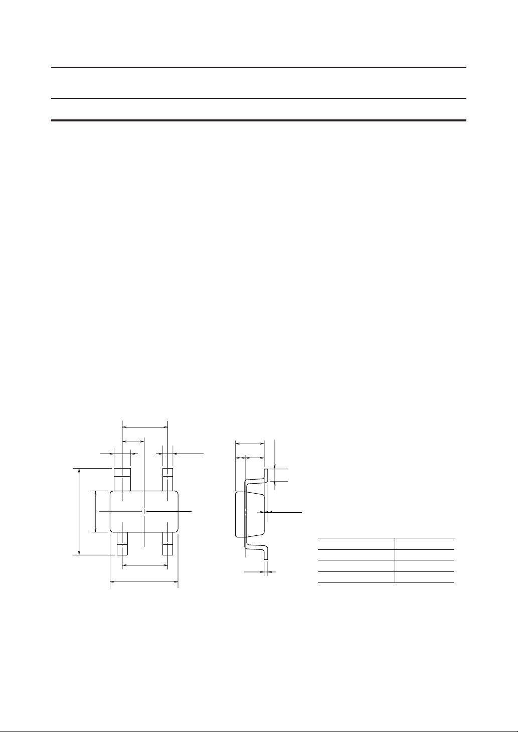
PACKAGE DIMENSIONS
1.8±0.1
0.85±0.05
+0.1
0.6
–0.05
3.0±0.2
1.5±0.15
1.9±0.1
2.8±0.15
0.4
+0.1
–0.05
1.1±0.15
0.36 0.74
+0.03
0.125
–0
(Unit: mm)
0.3 MIN
0 to 0.15
Package material
Lead frame material
Pin treatment
Solder plate thickness
Epoxy resin
42 alloy
Solder plating
5 mm or more
1/8
Page 2
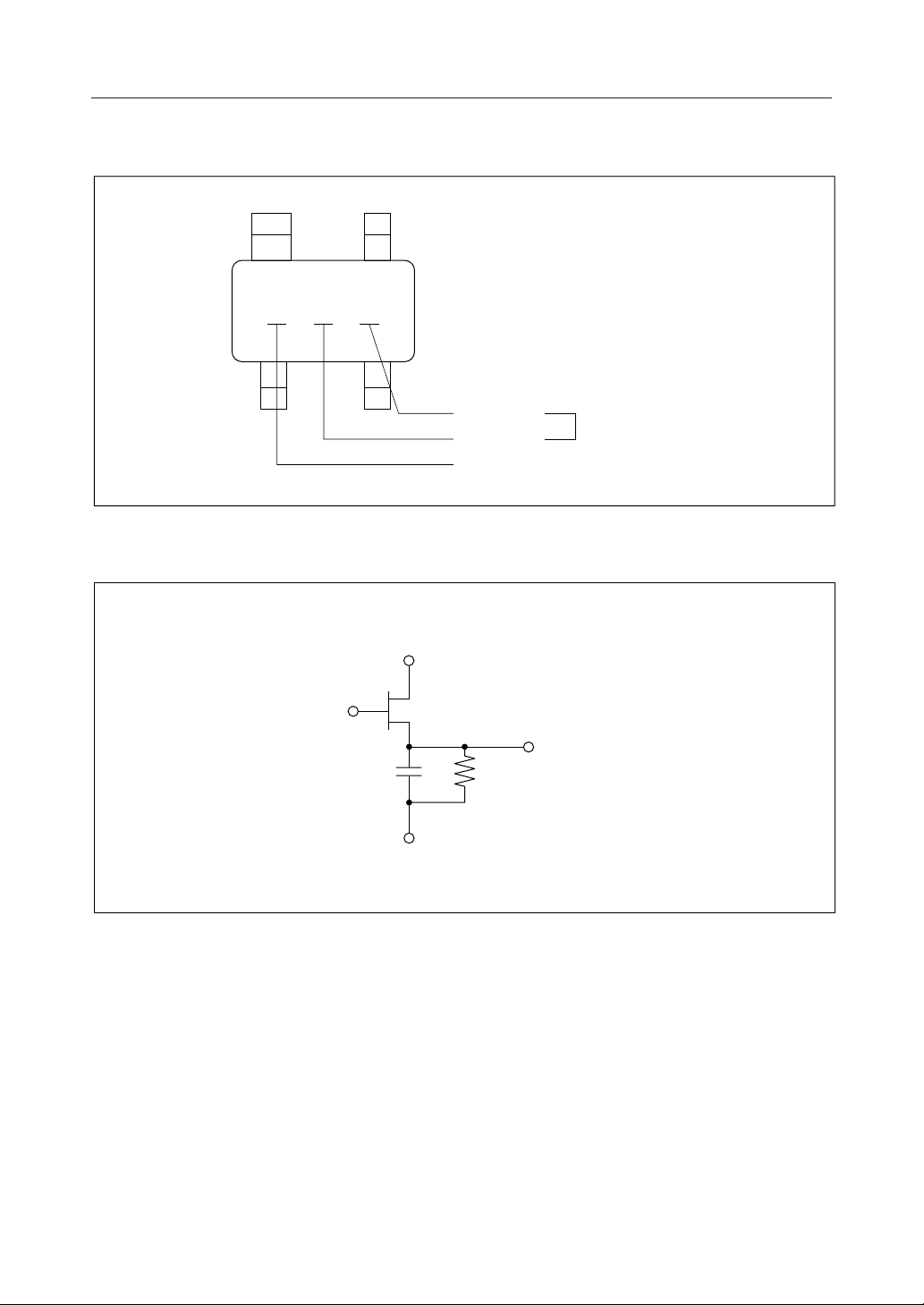
MARKING
(4) (3)
X
XF
KGF1521¡ electronic components
CIRCUIT
(1)
G(1)
(2)
D(3)
GND(4)
NUMERICAL
NUMERICAL
PRODUCT TYPE
S(2)
LOT
NUMBER
(1) Gate
(2) Source
(3) Drain
(4) GND
2/8
Page 3
ABSOLUTE MAXIMUM RATINGS
KGF1521¡ electronic components
Item
Drain-source voltage
Gate-source voltage
Drain current I
Total power dissipation
Channel temperature
Storage temperature T
Symbol Condition Max.Unit
V
DS
V
GS
DS
P
tot
T
ch
stg
Ta = 25°C
Ta = 25°C
V
V
Ta = 25°C 50mA —
Ta = 25°C
—
mW
°C
— 125°C
Min.
—
–3.0
—
—
–45
4.0
0.4
200
150
ELECTRICAL CHARACTERISTICS
(Ta = 25°C)
Item
Gate-source leakage current 30mA—VGS = –3 V —
Gate-drain leakage current 30mA—VGD = –6 V —
Drain-source leakage current 30mA—VDS = 3 V, VGS = –2 V —
Drain current —mA 15VDS = 3 V, VGS = 0 V 25
Operating current 2.5mA —(*1), P
Gate-source cut-off voltage –0.6V –1.4VDS = 3 V, IDS = 100 mA—
Transconductance —mS 14VDS = 3 V, IDS = 2 mA 17
Linear gain G
Output power —dBm
Third-order intercept point IP
Symbol Condition Max.Unit
I
GSS
I
GDO
I
DS(off)
I
DSS
V
GS(off)
g
P
I
D
m
LIN
O1
(*1)
3
= –20 dBm 2.0
IN
= –20 dBm
IN
dB
dBm ——12(*2), f2 = 1.901 GHz
Min.
—
–3.0
Typ.
1.8Noise figure F (*1) dB
0
2.5
—11.0 12.5(*1), P
*1 Self-bias condition: V
= 3 V ± 0.3 V, V
DD
= 0 V, f = 1.9 GHz
G
3/8
Page 4

RF CHARACTERISTICS
KGF1521¡ electronic components
4/8
Page 5

KGF1521¡ electronic components
5/8
Page 6

Typical S Parameters
Freq(MHz)
1000.0
1100.0
1200.0
1300.0
1400.0
1500.0
1600.0
1700.0
1800.0
1900.0
2000.0
2100.0
2200.0
2300.0
2400.0
2500.0
2600.0
2700.0
2800.0
2900.0
3000.0
MAG(S11) ANG(S11) MAG(S21) ANG(S21) MAG(S12) ANG(S12) MAG(S22) ANG(S22)
500.0
600.0
700.0
800.0
900.0
1.006
1.004
1.001
0.998
0.995
0.992
0.987
0.983
0.978
0.972
0.966
0.959
0.950
0.941
0.935
0.924
0.915
0.905
0.893
0.881
0.866
0.852
0.837
0.821
0.806
0.790
–9.13
–10.96
–12.83
–14.68
–16.53
–18.33
–20.18
–22.02
–23.88
–25.70
–27.62
–29.46
–31.22
–33.22
–35.13
–37.04
–38.95
–40.60
–42.34
–44.23
–15.91
–47.73
–49.40
–51.16
–52.74
–54.25
1.330
1.338
1.346
1.353
1.354
1.359
1.359
1.369
1.374
1.376
1.388
1.397
1.393
1.409
1.418
1.434
1.440
1.435
1.440
1.458
1.448
1.455
1.447
1.467
1.454
1.462
176.30
172.44
168.98
165.93
163.08
160.07
157.16
154.84
152.28
149.79
146.67
144.51
141.98
138.88
136.15
133.84
131.23
128.21
125.19
122.85
120.01
116.96
114.13
111.27
108.42
105.45
0.010
0.012
0.013
0.015
0.016
0.018
0.018
0.020
0.021
0.022
0.022
0.022
0.023
0.023
0.023
0.022
0.023
0.024
0.023
0.023
0.023
0.024
0.025
0.027
0.029
0.032
77.66
75.14
74.67
74.75
74.68
72.86
73.49
72.57
71.18
70.96
71.48
70.80
70.04
71.52
72.15
75.12
80.13
80.50
82.84
87.86
91.51
97.20
105.76
110.78
118.12
122.68
KGF1521¡ electronic components
= 3 V, ID = 2.23 mA
V
DD
0.939
0.937
0.934
0.933
0.932
0.930
0.927
0.926
0.925
0.922
0.920
0.918
0.914
0.911
0.910
0.905
0.903
0.900
0.894
0.892
0.887
0.883
0.879
0.874
0.871
0.868
–6.40
–7.42
–8.59
–9.60
–10.71
–11.75
–12.88
–13.89
–14.99
–16.04
–17.08
–18.12
–18.95
–20.20
–21.19
–22.16
–23.29
–24.24
–25.15
–26.13
–26.95
–27.96
–28.80
–29.63
–30.58
–31.21
6/8
Page 7

Typical S Parameters
V
= 3 V, ID = 2.23 mA
DD
Frequency : 0.5 to 3.0 GHz
Z0 = 50 W
KGF1521¡ electronic components
7/8
Page 8

Test Circuit and Bias Configuration for KGF1521 at 1.9 GHz
KGF1521¡ electronic components
IN
C
C
T
1
R
G
T1: Z0 = 75 W, E = 23 deg
T
: Z0 = 100 W, E = 2 deg
2
T
: Z0 = 100 W, E = 68 deg
3
T
= T8: Z0 = 100 W, E = 10 deg
4
C
= 1.40 pF, C2 = 1.35 pF
1
C
C(DC Block)
RFC = 60 nH, R
T
T
2
T
4
C
1
= 1000 pF, C
= 1000 W
G
3
(1) (3)
KGF
1521
(4)
T
B(By-pass)
T
T
9
6
5
T
8
C
2
T5: Z0 = 100 W, E = 87 deg
T
: Z0 = 100 W, E = 25 deg
6
T
: Z0 = 75 W, E = 20 deg
7
T
: Z0 = 100 W, E = 5 deg
9
= 1000 pF, C
F(Feed through)
T
RFC
C
7
B
C
C
C
= 1000 pF
OUT
F
V
DD
8/8
 Loading...