

Page 1
Features
■
80MHz full-power bandwidth (20Vpp, 100Ω)
■
200mA output current
■
0.4% settling in 10ns
■
6000V/µs slew rate
■
4ns rise and fall times (20V)
■
Direct replacement for CLC103
Applications
■
Coaxial line driving
■
DAC current to voltage amplifier
■
Flash A to D driving
■
Baseband and video communications
■
Radar and IF processors
General Description
The KH103 is a high-power, wideband op amp designed
for the most demanding high-speed applications. The
wide bandwidth, fast settling, linear phase, and very
low harmonic distortion provide the designer with
the signal fidelity needed in applications such as driving
flash A to Ds. The 80MHz full-power bandwidth and
200mA output current of the KH103 eliminate the
need for power buffers in most applications; the
KH103 is an excellent choice for driving large highspeed signals into coaxial lines.
In the design of the KH103 special care was taken in
order to guarantee that the output settle quickly to
within 0.4% of the final value for use with ultra fast
flash A to D converters. This is one of the most
demanding of all op amp requirements since settling
time is affected by the op amps bandwidth, passband
gain flatness, and harmonic distortion. This high
degree of performance ensures excellent performance
in many other demanding applications as well.
The dynamic performance of the KH103 is based on a
current feedback topology that provides performance
far beyond that available from conventional op amp
designs. Unlike conventional op amps where optimum
gain-bandwidth product occurs at a high gain, minimum
settling time at a gain of -1, and maximum slew rate
at a gain of +1, the KH103 provides consistent
predictable performance across its entire gain range.
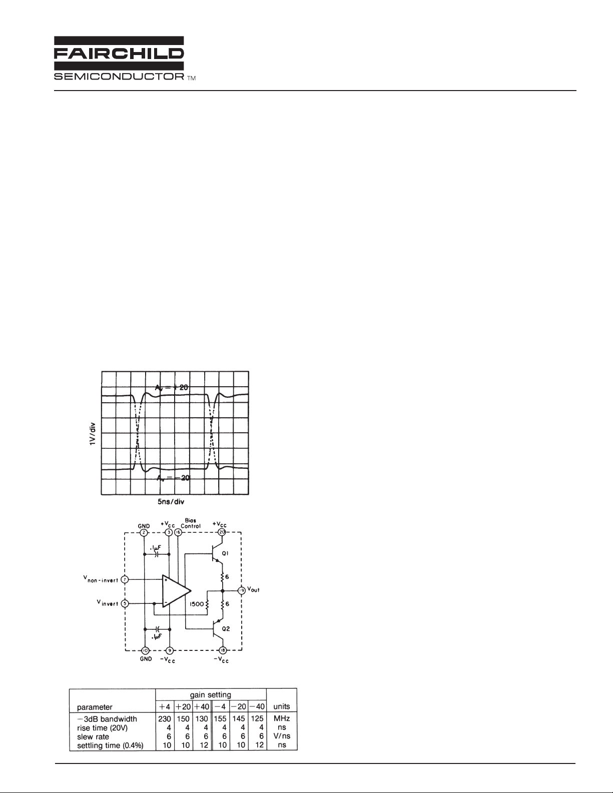
For example, the table below shows how the -3dB
bandwidth remain nearly constant over a wide range
of gains. And since the amplifier is inherently stable,
no external compensation is required. The result is
shorter design time and the ability to accommodate
design changes (in gain, for example) without loss of
performance or redesign of compensation circuits.
The KH103 is constructed using thin film resistor/
bipolar transistor technology, and is available in the
following versions:
KH103AI -25°C to +85°C 24-pin Ceramic DIP
KH103AK -55°C to +125°C 24-pin Ceramic DIP,
features burn-in and
hermetic testing
KH103AM -55°C to +125°C 24-pin Ceramic DIP,
environmentally screened
and electronically tested
to MIL-STD-883
KH103
Fast Settling, High Current Wideband Op Amp
www.fairchildsemi.com
REV. 1A February 2001
Small Signal Pulse Response
Typical Performance
Page 2
DATA SHEET KH103
2 REV. 1A February 2001
Absolute Maximum Ratings
VCC(reversed supplies will destroy part) ±20V
junction temperature (see thermal model) +175°C
thermal resistance see thermal model
storage temperature -65°C to +150°C
lead temperature (soldering 10s) +300°C
output current ±200mA
operating temperature: AI -25°C to +85°C
AK, AM -55C to +125°C
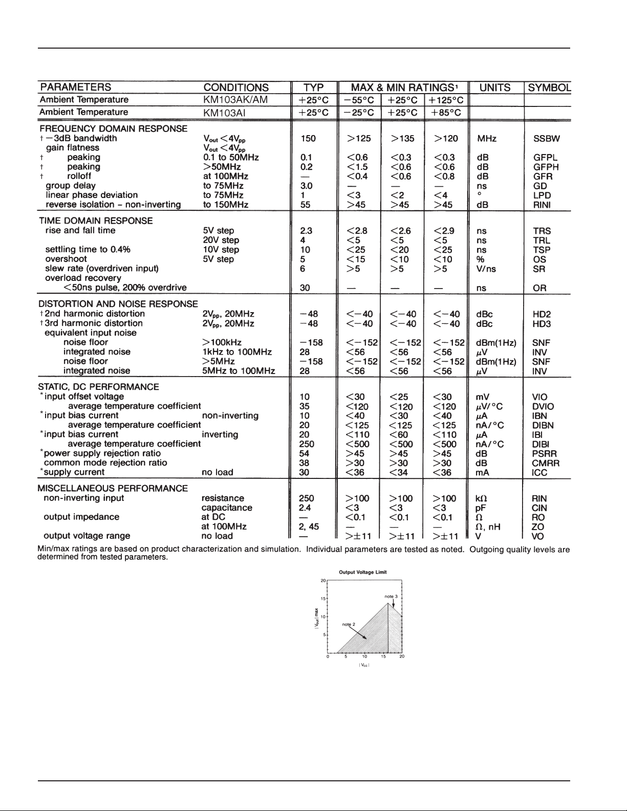
KH103 Electrical Characteristics
(Av= +20V, VCC= ±15V, RL= 100Ω; unless noted)
Notes
1) * AI, AK, AM 100% tested at +25°C
✝ AK, AM 100% tested at at +25°C and sample tested at -55°C and +125°C
✝ AI sample tested at +25°C
2) This rating protects against damage to the input stage caused by saturation of either the input or output stages. Under
transient conditions not exceeding 1
µs (duty cycle not exceeding 10% maximum input voltage may be as large as twice the maximum V
cm
should never exceed ±5V. (Vcmis the voltage at the non-inverting input, pin 7).
3) This rating protects against exceeding transistor collector-emitter breakdown ratings. Recommended V
CC
is ±15V.
Page 3
KH103 DATA SHEET
REV. 1A February 2001 3
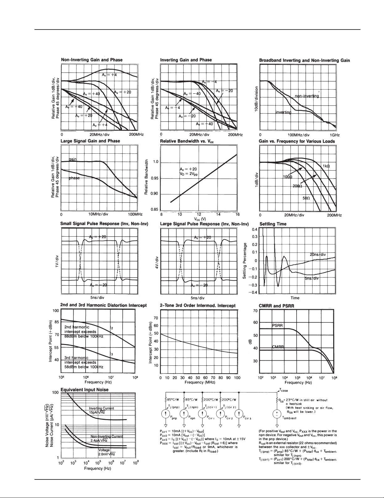
KH103 Performance Characteristics
(Av= +20°C, VCC= ±15V, RL= 100Ω; unless noted)
Page 4
DATA SHEET KH103
4 REV. 1A February 2001
KH103 Operation
The KH103 is based on a unique design which uses
current feedback instead of the usual voltage feedback.
This design provides dynamic performance far beyond
that previously available, yet it is used basically the same
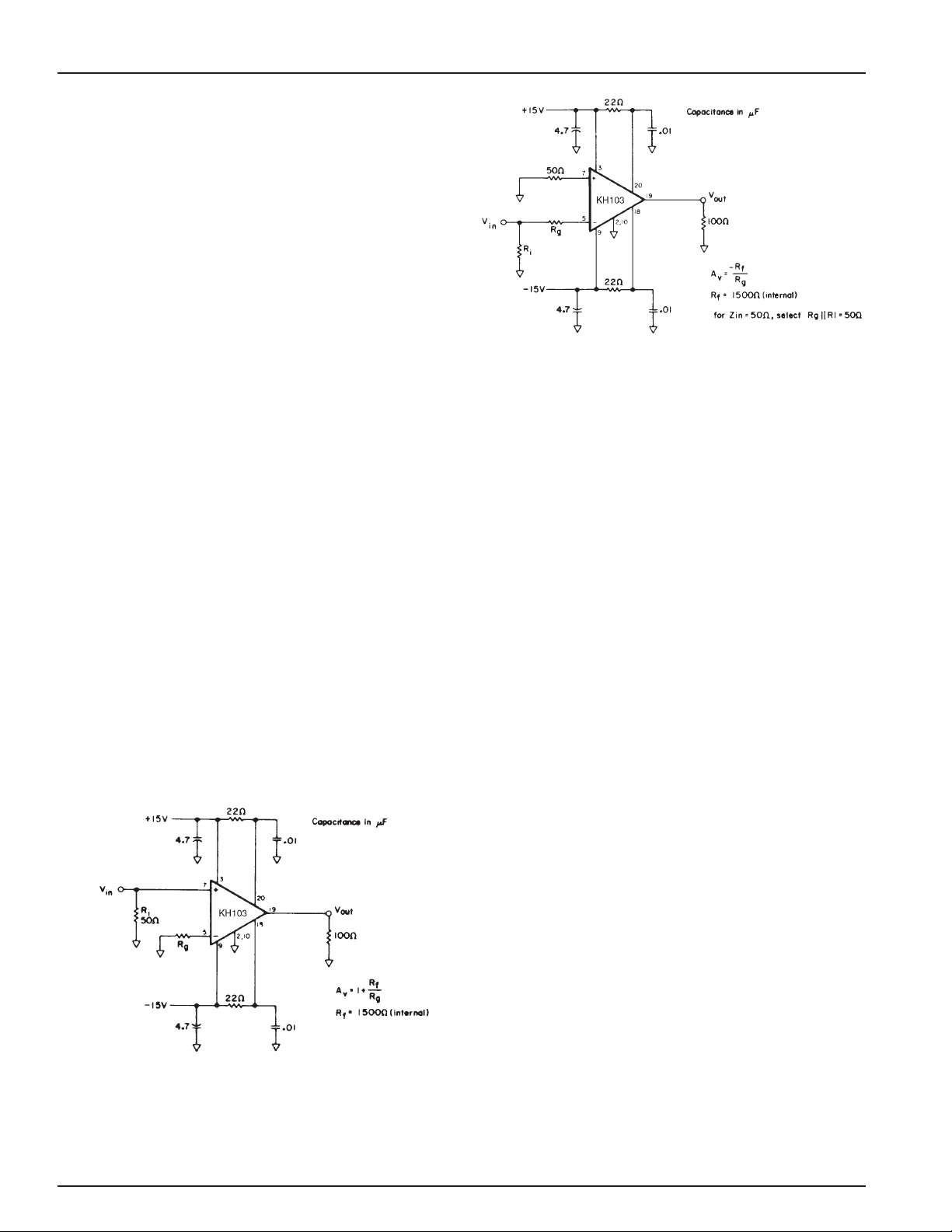
as the familiar voltage-feedback op amp (see the gain
equations above).
Layout Considerations
To obtain optimum performance from any circuit
operating at high frequencies, good PC layout is
essential. Fortunately, the stable, well-behaved response
of the KH103 makes operation at high frequencies less
sensitive to layout than is the case with other wideband
op amps, even though the KH103 has a much wider
bandwidth.
In general, a good layout is one which minimizes the
unwanted coupling of a signal between nodes in a circuit.
A continuous ground plane from the signal input to output
on the circuit side of the board is helpful. Traces should
be kept short to minimize inductance. If long traces are
needed, use microstrip transmission lines which are
terminated in their characteristic impedance. At some
high-impedance nodes, or in sensitive areas such as
near pin 5 of the KH103, stray capacitance should be
kept small by keeping nodes small and removing ground
plans directly around the node.
The ±VCCconnections to the KH103 are internally
bypassed to ground with 0.1µF capacitors to provide
good high-frequency decoupling. It is recommended that
1µF or larger tantalum capacitors be provided for lowfrequency decoupling. The 0.01µF capacitors shown at
pins 18 and 20 in figures 1 and 2 should be kept within
0.1” of those pins. A wide strip of ground plane should be
provided for a signal return path between the load-resistors ground and these capacitors.
Figure 1: Recommended Non-Inverting Gain Circuit
Figure 2: Recommended Inverting Gain Circuit
Since the layout of the PC board forms such an important
part of the circuit, much time can be saved if prototype
amplifier boards are tested early in the design stage.
Settling Time, Offset, and Drift
After an output transition has occurred. the output settles
very rapidly to the final value and no change occurs for
several microseconds. Thereafter, thermal gradients
inside the KH103 will cause the output to begin to drift.
When this cannot be tolerated, or when the initial offset
voltage and drift is unacceptable, use of a composite
amplifier is advised.
A composite amplifier can also be referred to as a feedforward amplifier. Most feed-forward techniques such as
those used In the vast majority of wideband op amps
involve the use of a wideband AC-coupled channel in parallel with a low-bandwidth, high-gain DC-coupled amplifier. For the composite amplifier suggested for use with
the KH103, the KH103 replaces the wideband AC-coupled amplifier and a low-cost monolithic op amp is used
to supply high open-loop gain at low frequencies. Since
the KH103 is strictly DC coupled throughout, crossover
distortion of less than 0.01dB and 1° results.
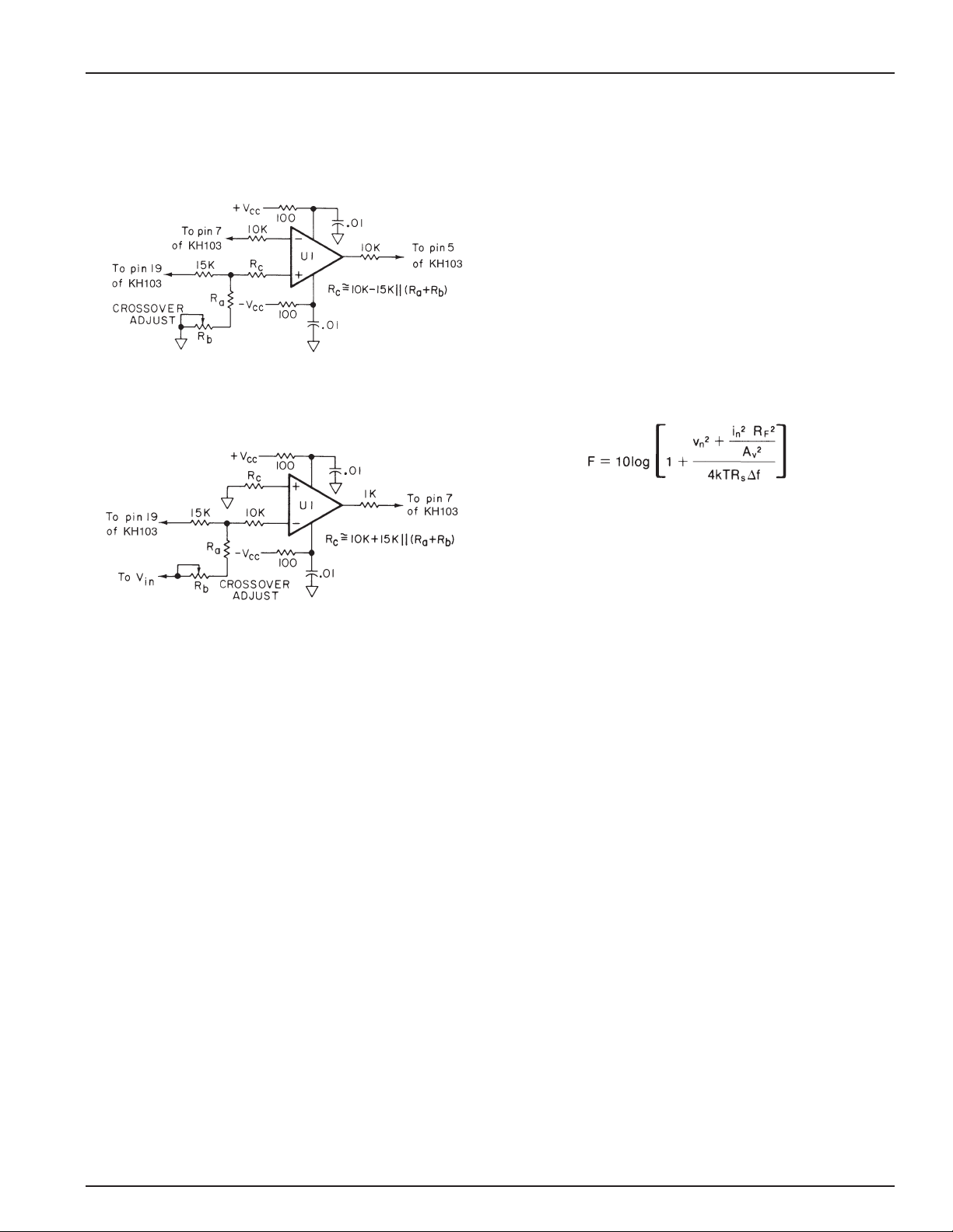
For composite operation in the non-inverting mode, the
circuit in Figure 1 should be modified by the addition of
the circuit shown in Figure 3. For Inverting operation,
modify the circuit in Figure 2 by the addition of the circuit
in Figure 4. Keep all resistors which connect to the
KH103 within 0.2” of the KH103 pins. The other side of
these resistors should likewise be as close to U1 as
possible. For good overall results, U1 should be similar
to the LF356; this gives 5mV/°C input offset drift and the
crossover frequency occurs at about 2MHz. Since U1
has a feedback network composed of Ra+ Rband a
15kΩ resistor, which is in parallel with Rgand the internal
1.5kΩ feedback resistor of the KH103, Rbmust be
adjusted to match the feedback ratios of the two networks. This in done by driving the composite amplifier
Page 5
REV. 1A February 2001 5
KH103 DATA SHEET
with a 70kHz square wave large enough to produce a
transition from +5V to -5V at the KH103 output and
adjusting Rbuntil the output of U1 is at a minimum. R
a
should be about 9.5Rgfor bad results; thus, Rbshould be
adjusted around the value of 0.5Rg.
Figure 3: Non-Inverting Gain Composite Amplifier
to be Used with Figure 1 Circuit
Figure 4: Inverting Gain Composite Amplifier to be
Used with Figure 2 Circuit
Bias Control
In normal operation, the bias control pin (pin 16) is left
unconnected. However, if control over the bias of the
amplifier is desired, the bias control pin may be driven
with a TTL signal; a TTL high level will turn the amplifier
off.
Distortion and Noise
The graphs of intercept point versus frequency on the
page 3 make it easy to predict the distortion at any frequency, given the output voltage of the KH103. First convert the output voltage Voto V
rms
= (Vpp/2√2) and then to
P = (10log10(20V
rms
2
)) to get the output power in dBm.
At the frequency of interest, its 2nd harmonic will be S2=
(I2- P) dB below the level of P. Its third harmonic will be
S3= 2(I3- P) dB below the level of P, as will the two-tone
third order intermodulation products. These approximations are useful for P < -1dB compression levels.
Approximate noise figure can determined for the KH103
using the Equivalent Input Noise graph on page 3. The
following equation can be used to determine noise figure
(F) in dB.
where vnis the rms noise voltage and inis the rms noise
current. Beyond the breakpoint of the curves (i.e. where
they are flat) broadband noise figure equals spot noise,
so ∆f should equal one (1) and vnand inshould be read
directly off the graph. Below the breakpoint, the noise
must be integrated and ∆f set to the appropriate bandwidth.
Page 6
DISCLAIMER
FAIRCHILD SEMICONDUCTOR RESERVES THE RIGHT TO MAKE CHANGES WITHOUT FURTHER NOTICES TO ANY PRODUCTS HEREIN TO IMPROVE RELIABILITY, FUNCTION OR DESIGN. FAIRCHILD
DOES NOT ASSUME ANY LIABILITY ARISING OUT OF THE APPLICATION OR USE OF ANY PRODUCT OR CIRCUIT DESCRIBED HEREIN; NEITHER DOES IT CONVEY ANY LICENSE UNDER ITS PATENT
RIGHTS, NOR THE RIGHTS OF OTHERS.
LIFE SUPPORT POLICY
FAIRCHILD’S PRODUCTS ARE NOT AUTHORIZED FOR USE AS CRITICAL COMPONENTS IN LIFE SUPPORT DEVICES OR SYSTEMS WITHOUT THE EXPRESS WRITTEN APPROVAL OF THE PRESIDENT
OF FAIRCHILD SEMICONDUCTOR CORPORATION. As used herein:
1. Life support devices or systems are devices or systems which, (a) are intended for
surgical implant into the body, or (b) support or sustain life, and (c) whose failure to
perform when properly used in accordance with instructions for use provided in the
labeling, can be reasonably expected to result in a significant injury of the user.
2. A critical component in any component of a life support device or system whose
failure to perform can be reasonably expected to cause the failure of the life
support device or system, or to affect its safety or effectiveness.
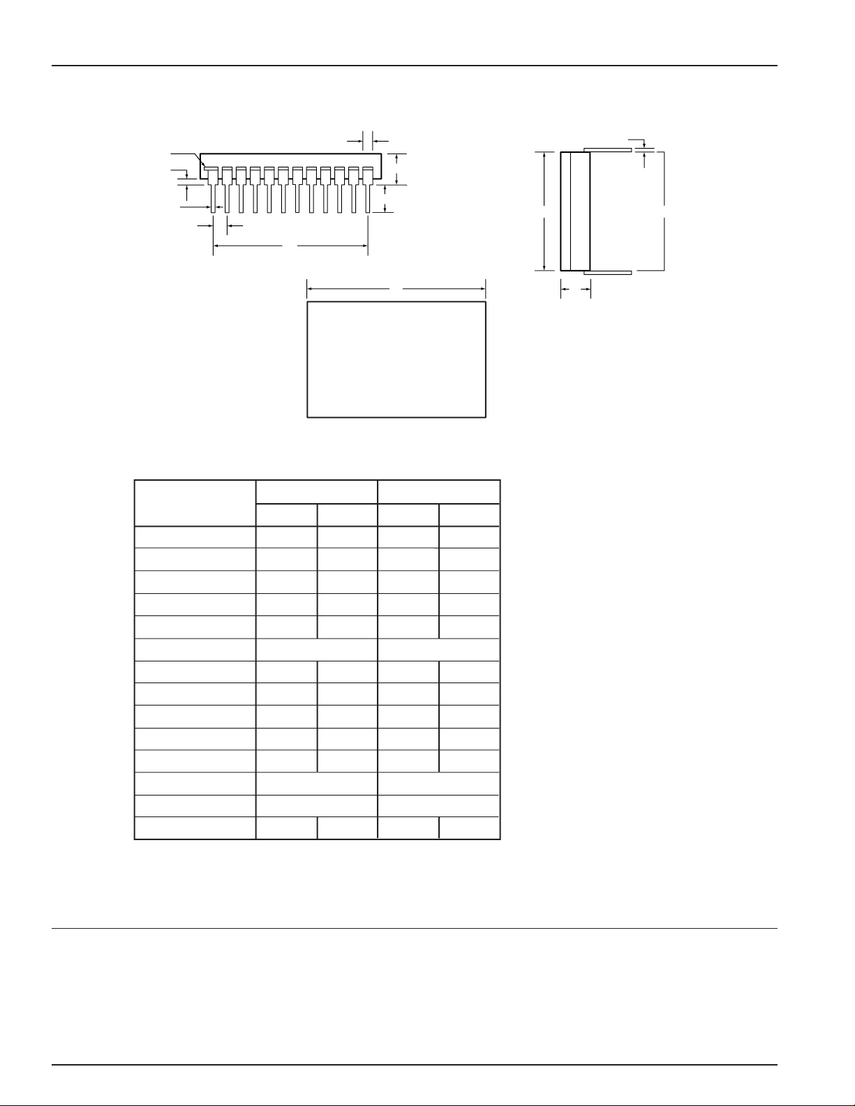
KH103 Package Dimensions
DATA SHEET KH103
www.fairchildsemi.com © 2001 Fairchild Semiconductor Corporation
Pin #1
Index
Q
b
Symbol
e
D1
Inches Milimeters
b1
A
L
D
Minimun Maximum Minimum Maximum
A-Metal Lid 0.180 0.240 4.57 6.10
A-Ceramic Lid 0.195 0.255 4.95 6.48
A1-Metal Lid 0.145 0.175 3.68 4.45
A1-Ceramic Lid 0.160 0.190 4.06 4.83
b 0.014 0.026 0.36 0.66
b1 0.050 BSC 1.27 BSC
c 0.008 0.018 0.20 0.46
D 1.275 1.310 33.39 33.27
D1 1.095 1.105 27.81 28.07
E 0.785 0.815 19.94 20.70
E1 0.790 0.810 20.07 20.57
e 0.100 BSC 2.54 BSC
L 0.165 BSC 4.19 BSC
Q 0.015 0.075 0.38 1.91
C
E
A1
NOTES:
NOTES:
Seal: seam weld (AM, AK), epoxy (AI)
Lead finish: gold finish
Package composition:
Package: ceramic
Lid: kovar/nickel (AM, AK), ceramic (AI)
Leadframe: alloy 42
Die attach: epoxy
E1
 Loading...