

Page 1
Features
■
165MHz closed-loop – -3dB bandwidth
■
15ns settling to 0.05%
■
1mV input offset voltage, 10µV/°C drift
■
100mA output current
■
Excellent AC and DC linearity
■
Direct replacement for CLC231
Applications
■
Driving flash A/D converters
■
Precision line driving
(a gain of 2 cancels matched-line losses)
■
DAC current-to-voltage conversion
■
Low-power, high-speed applications (50mW @ ±5V)
General Description
The KH231 Buffer/Amplifier is a wideband operational
amplifier designed specifically for high-speed, lowgain applications. The KH231 is based on a current
feedback op amp topology-a unique design that both
eliminates the gain-bandwidth tradeoff and permits
unprecedented high-speed performance. (See table below.)
The KH231 Buffer/Amplifier is the ideal design alternative to low precision open-loop buffers and oscillationprone conventional op amps. The KH231 offers precise
gains from ±1.000 to ±-5.000 and linearity that is a
true 0.1%-even for demanding 50
Ω loads. Open-loop
buffers, on the other hand, offer a nominal gain of
0.95 ±0.03 and a linearity of only 3% for typical loads.
A buffer’s settling time may look impressive but it is
usually specified at unrealistically large load resistances or when the effects of thermal tail are not
included; the KH231 Buffer/Amplifier settles to 0.05%
in 15ns-while driving a 100Ω load.
Offsets and drifts, usually a low priority in conventional high-speed op amp designs, were not ignored
in the KH231; the input offset voltage is typically 1mV
and input offset voltage drift is only 10µV/°C. The
KH231 is stable and oscillation-free across the entire
gain range and since it’s internally compensated, the
user is saved the trouble of designing external compensation networks and having to “tweak” them in
production. The absence of a gain-bandwidth tradeoff in the KH231 allows performance to be predicted
easily; the table below shows how the bandwidth is
affected very little by changing the gain setting.
The KH231 is constructed using thin film resistor/bipolar
transistor technology, and is available in the following
versions:
The KH231 is constructed using thin film resistor/bipolar
transistor technology, and available in these versions:
KH231AI -25°C to +85°C 12-pin TO-8 can
KH231AK -55°C to +125°C 12-pin TO-8 can, features
burn-in & hermetic testing
KH231AM -55°C to +125°C 12-pin TO-8 can,
environmentally
screened and electrically
tested to MIL-STD-883
KH231HXC -55°C to +125°C SMD#: 5962-8959401HXC
KH231HXA -55°C to +125°C SMD#: 5962-8959401HXA
KH231
Fast Settling, Wideband Buffer/Amplifier (Av= ±1 to ±5)
www.fairchildsemi.com
REV. 1A February 2001
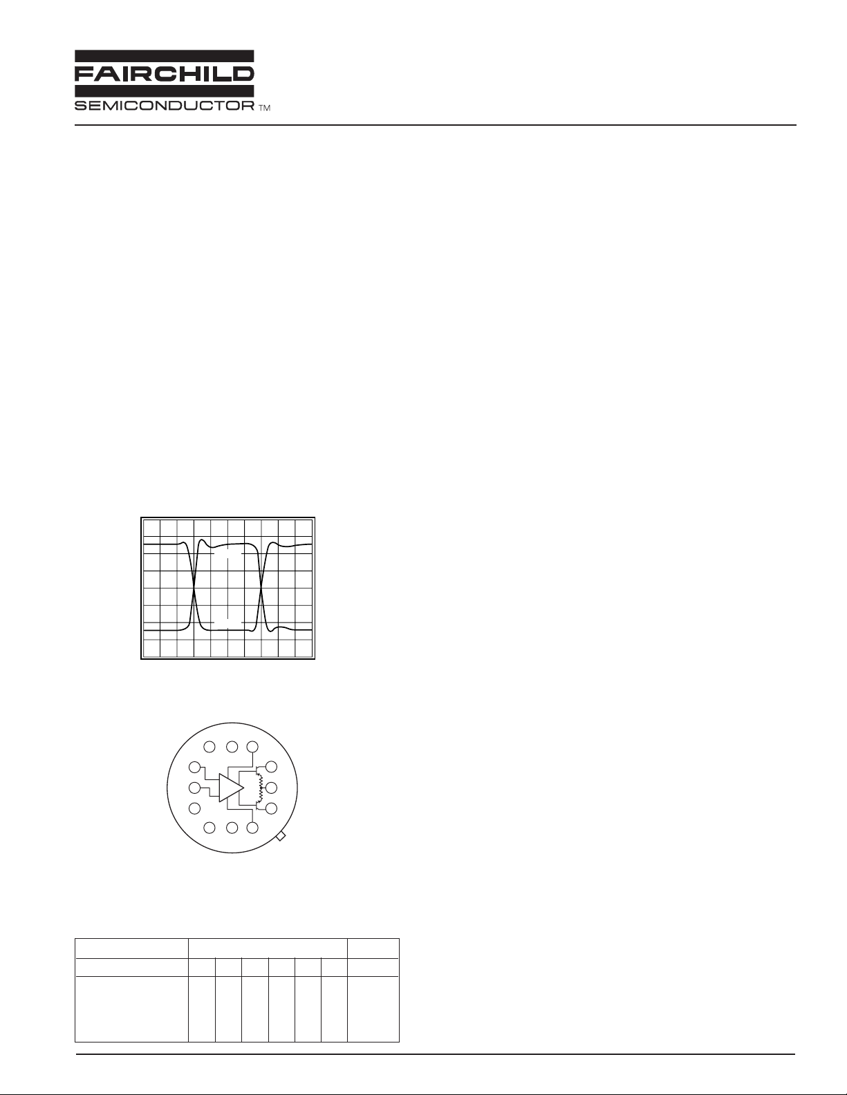
Small Signal Pulse Response
Output Voltage (400mV/div)
Time (5ns/div)
Av = -2
Av = 2
Supply
Voltage
8
Adjust
7
GND
9
-V
CC
2
Adjust
3
GND
1
+V
CC
6
V+
5
V-
4
NC
10
-V
CC
V
o
+V
CC
11
12
4
4
Collector
Supply
Output
Collector
Supply
Supply
Voltage
I
CC
Adjust
I
CC
Adjust
Case
ground
Non-Inverting
Input
Inverting
Input
Not
Connected
Case
ground
+
-
Bottom View
Pins 2 and 8 are used to adjust the supply current or to adjust the offset voltage (see text). These pins are normally left unconnected.
Typical Performance
Gain Setting
Parameter 125-1-2-5Units
-3dB bandwidth 180 165 130 165 150 115 MHz
rise time (2V) 1.8 2.0 2.5 2.0 2.2 2.9 ns
slew rate 2.5 3.0 3.0 3.0 3.0 3.0 V/ns
settling time (to 0.1%) 12 12 12 12 12 15 ns
Page 2

2 REV. 1A February 2001
DATA SHEET KH231
PARAMETERS CONDITIONS TYP MIN & MAX RATINGS UNITS SYM
Ambient Temperature KH231AI +25°C -25°C +25°C +85°C
Ambient Temperature KH231AK/AM/HXC/HXA +25°C -55°C +25°C +125°C
FREQUENCY DOMAIN RESPONSE
✝ -3dB bandwidth (note 2) V
o
≤2V
pp
165 >145 >145 >120 MHz SSBW
large-signal bandwidth V
o
≤10V
pp
95 >80 >80 >60 MHz FPBW
gain flatness (note 2) V
o
≤2V
pp
✝ peaking 0.1 to 50MHz 0.1 <0.6 <0.3 <0.6 dB GFPL
✝ peaking >50MHz 0.1 <1.5 <0.3 <0.8 dB GFPH
✝ rolloff at 100MHz 0.4 <0.6 <0.6 <1.0 dB GFR
group delay to 100MHz 3.5 ± 0.5 –––ns GD
linear phase deviation to 100MHz 0.5 <2.0 <2.0 <2.0 ° LPD
reverse isolation
non-inverting 53 >43 >43 >43 dB RINI
inverting 36 >26 >26 >26 dB RIIN
TIME DOMAIN RESPONSE
rise and fall time 2V step 2.0 <2.4 <2.3 <2.7 ns TRS
10V step 5.0 <7.0 <6.5 <6.5 ns TRL
settling time to 0.05% 5V step 15 –––ns TS
to 0.1% 2.5V step 12 <22 <17 <22 ns TSP
overshoot 5V step 5 <15 <10 <15 % OS
slew rate (overdriven input) 3.0 >2.5 >2.5 >1.8 V/ns SR
overload recovery <1% error
<50ns pulse, 200% overdrive 120 –––ns OR
NOISE AND DISTORTION RESPONSE
✝ 2nd harmonic distortion 0dBm, 20MHz -55 <-47 <-47 <-47 dBc HD2
✝ 3rd harmonic distortion 0dBm, 20MHz -59 <-47 <-47 <-47 dBc HD3
equivalent input noise
noise floor >5MHz -153 <-150 <-150 <-150 dBm(1Hz) SNF
integrated noise 5MHz to 200MHz 70 <100 <100 <100
µVrms INV
STATIC, DC PERFORMANCE
* input offset voltage 1 <4.0 <2.0 <4.5 mV VIO
average temperature coefficient 10 <25 <25 <25
µV/°C DVIO
* input bias current non-inverting 5.0 <29 <21 <31
µA IBN
average temperature coefficient 50 <125 <125 <125 nA/°C DIBN
* input bias current inverting 10 <31 <15 < 35
µA IBI
average temperature coefficient 125 <200 <200 <200 nA/°C DIBI
* power supply rejection ratio 50 >45 >45 >45 dB PSRR
common mode rejection ratio 46 >40 >40 >40 dB CMRR
* supply current no load 18 <22 <22 <22 mA ICC
MISCELLANEOUS PERFORMANCE
non-inverting input resistance DC 400 >100 >200 >400 kΩ RIN
non-inverting input capacitance 1.3 <2.5 <2.5 <2.5 pF CIN
output impedance @ 100MHz 5, 37 –––
Ω, nH RO
output voltage range no load ±12 >±11 >±11 >±11 V VO
Min/max ratings are based on product characterization and simulation. Individual parameters are tested as noted. Outgoing quality levels are
determined from tested parameters.
Absolute Maximum Ratings Recommended Operating Conditions
V
CC
±20V V
CC
±5V to ±15V
I
o
±100mA I
o
±75mA
common mode input voltage, V
o
(see Vcmand V
o
common mode input voltage ±(|VCC| -5)V
limits plot on page 3) gain range ±1 to ±5
differential input voltage ±3V
thermal resistance (see thermal model)
junction temperature +175°C
operating temperature AI: -25°C to +85°C
AK/AM: -55°C to +125°C
storage temperature -65°C to +150°C
lead temperature (soldering 10s) +300°C
KH231 Electrical Characteristics
(
T
A
= +25°C,
A
v
= +2V, VCC= ±15V, RL= 100Ω, Rf= 250Ω; unless specified)
note 1: * AI/AK/AM/HXC/HXA 100% tested at +25°C
✝ AK/AM/HXC/HXA 100% tested at +25°C and sample
tested at -55°C and +125°C
✝ AI sample tested at +25°C
note 2: The output amplitude used in testing is 0.63Vpp. Performance
is guaranteed for conditions listed.
note 3: In the noninverting configuration, care should be taken when
choosing Ri, the input impedance setting resistor; bias
currents of typically 5µA but as high as 24µA can create an
input signal large enough to cause overload. It is therefore
recommended that Ri< (VCC/Av)/24µA.
note 4: These ratings protect against damage to the input stage
caused by saturation of either the input or output stages at
lower supply voltages, and against exceeding transistor
collector-emitter breakdown ratings at high supply voltages.
V
out(max)
is calculated by assuming no output saturation.
Saturation is allowed to occur up to this calculated level of
V
out.Vcm
is defined as the voltage at the non-inverting
input, pin 6.
Page 3
KH231 DATA SHEET
REV. 1A February 2001 3
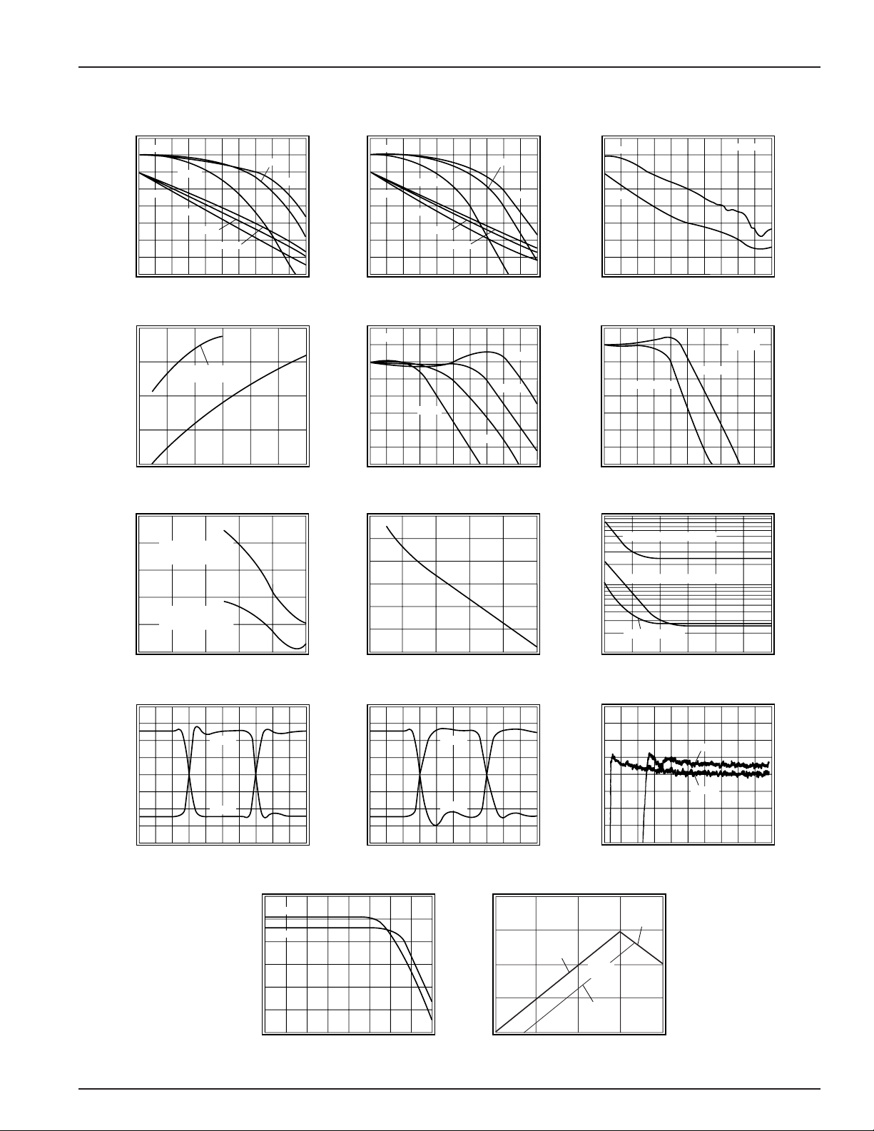
KH231 Typical Performance Characteristics
(TA= +25°C, Av= +2, VCC= ±15V, RL= 100Ω,
R
f
= 250Ω
; unless specified)
Non-Inverting Frequency Response
Gain
Av = 5
Phase
Av = 5
Av = 2
Av = 1
Normalized Magnitude (1dB/div)
0
100
Frequency (MHz)
Bandwidth vs. V
1.2
1.0
0.8
0.6
Relative Bandwidth
0.4
4 6 8 10 12 14 16
CC
Pins 1 and 2 Shorted
Pins 8 and 9 shorted
±VCC (V)
2nd and 3rd Harmonic Distortion Intercept
130
110
2nd harmonic intercept
exceeds +120dBm
90
below 350KHz
I
2
70
3rd harmonic intercept
50
Intercept Point (+dBm)
30
1k 10k 100k 1M 10M 100M
exceeds +65dBm
below 350KHz
I
3
Frequency (Hz)
Small Signal Pulse Response
Av = 2
Av = -2
Output Voltage (400mV/div)
Time (5ns/div)
Av = 2
Phase (45 deg/div)
Av = 1
200
Inverting Frequency Response
Gain
Phase
Av = -5
Av = -5
Av = -2
Av = -1
Normalized Magnitude (1dB/div)
0
100
Frequency (MHz)
Frequency Response vs. R
Av = 2
(1dB/div)
0
RL = 50
RL = 100
125
Frequency (MHz)
2-Tone, 3rd Order Intermod. Intercept
50
45
40
35
30
Intercept Point (+dBm)
25
20
20 40 60 80
0
Frequency (MHz)
Large Signal Pulse Response
Av = 2
Av = -2
Output Voltage (2V/div)
Time (5ns/div)
L
Av = -2
RL = 1K
RL = 200
Av = -1
200
250
Av = 2
100
Broadband Gain and Phase
Phase (45 deg/div)
Phase
Magnitude (10dB/div)
0
Full Power Gain vs. Frequency
(1dB/div)
0
Equivalent Input Noise
100
10
Noise Voltage (nV/√Hz)
1
100
Settling Time
0.20
0.15
0.10
0.05
0
-0.05
Settling Error (%)
-0.10
-0.15
-0.20
Gain
500
Frequency (MHz)
Non-Inverting
100
Frequency (MHz)
Inverting Current 23.8pA/√Hz
Non-Inverting Current 2.5pA/√Hz
Voltage 2.8nV/√Hz
1k 10k 100k 1M
Frequency (Hz)
50ns/div
Time (ns)
Inverting
5ns/div
V
Av = 2
Av = 2
= 10V
o
10M
Phase (180 deg/div)
1000
pp
200
100
Noise Current (pA/√Hz)
10
1
100M
CMRR and PSRR
PSRR
50
CMRR
40
30
20
PSRR/CMRR (dB)
10
1 10 100 1k 10k 100k
Frequency (Hz)
1M 10M
100M
Vcm and Vo Voltage Limits
20
15
|V
| max
10
Indicated Voltage
5
0
05 10
out
|±VCC| (V)
note 4
on page 2
|Vcm| max
|V
| max
out
| max
|V
cm
20
15
Page 4
DATA SHEET KH231
4 REV. 1A February 2001
Operation
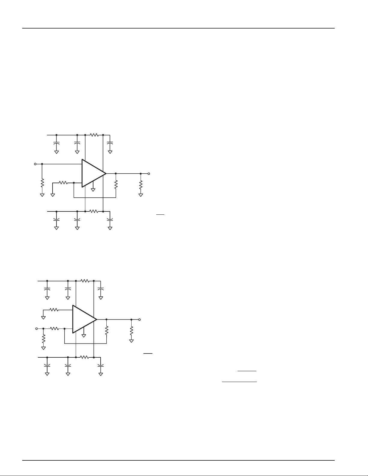
The KH231 Buffer/Amplifier is based on the current feedback op amp topology, a design that uses current feedback instead of the usual voltage feedback.
The use of the KH231 is basically the same as that of the
conventional op amp (see Figures 1 and 2). Since the
device is designed specifically for low gain applications,
the best performance is obtained when the circuit is used
at gains between ±1 and ±5. Additionally, performance is
optimum when a 250Ω feedback resistor is used.
Figure 1: Recommended non-inverting gain circuit
Figure 2: Recommended inverting gain circuit
Layout Considerations
To assure optimum performance the user should follow
good layout practices which minimize the unwanted
coupling of signals between nodes. During initial breadboarding of the circuit use direct point to point wiring,
keeping the lead lengths to less than 0.25”. The use of
solid, unbroken ground plane is helpful. Avoid wire-wrap
type pc boards and methods. Sockets with small, short
pin receptacles may be used with minimal performance
degradation although their use is not recommended.
During pc board layout keep all traces short and direct
The resistive body of Rgshould be as close as possible
to pin 5 to minimize capacitance at that point. For the
same reason, remove ground plane from the vicinity of
pins 5 and 6. In other areas, use as much ground plane
as possible on one side of the board. It is especially
important to provide a ground return path for current from
the load resistor to the power supply bypass capacitors.
Ceramic capacitors of 0.01 to 0.1µf (with short leads)
should be less than 0.15 inches from pins 1 and 9.
Larger tantalum capacitors should be placed within one
inch of these pins. VCCconnections to pins 10 and 12
can be made directly from pins 9 and 1, but better supply
rejection and settling time are obtained if they are
separately bypassed as in figures 1 and 2. To prevent
signal distortion caused by reflections from impedance
mismatches, use terminated microstrip or coaxial cable
when the signal must traverse more than a few inches.
Since the pc board forms such an important part of the
circuit, much time can be saved if prototype boards of any
high frequency sections are built and tested early in the
design phase. Evaluation boards designed for either
inverting or non-inverting gains are available.
Distortion and Noise
The graphs of intercept point, I2and I3, versus
frequency on the preceding page make it easy to predict
the distortion at any frequency given the output voltage of
the KH231. First, convert the output voltage (Vo) to V
rms
= (Vpp/2√2) and then to P = [(10log10(20V
rms
2
)] to get the
power output in dBm. At the frequency of interest, its 2nd
harmonic will be S2= (I2-P)dB below the level of P. Its
third harmonic will be S3= 2(I3- P)dB below P, as will the
two-tone third order intermodulation products. These
approximations are useful for P < -1dB compression levels.
Approximate noise figure can be determined for the
KH231 using the equivalent input noise graph on the
preceding page. The following equation can be used to
determine noise figure (F) in dB.
Where Vnis the rms noise voltage and inis the rms noise
current. Beyond the breakpoint of the curves (i.e., where
they are flat), broadband noise figure equals spot noise figure, so ∆f should equal one (1) and Vnand inshould be
read directly off the graph. Below the breakpoint, the noise
must be integrated and ∆f set to the appropriate bandwidth.
6
KH231
5
0.1
+
-
33Ω
1
9
33Ω
3,7
12
10
.01
Capactance in µF
11
250Ω
.01
V
R
L
100Ω
A
= 1+
v
Rf = 250Ω
o
R
f
R
g
+15V
V
in
R
49.9Ω
-15V
3.9
i
R
3.9
0.1
g
6
5
0.1
33Ω
1
+
KH231
-
3,7
9
33Ω
12
10
.01
Capactance in µF
11
250Ω
A
.01
Rf = 250Ω
For Z
R
V
o
R
L
100Ω
R
=−
v
R
= 50Ω, select
in
|| Ri = 50Ω
g
f
g
+15V
V
in
-15V
3.9
R
i
100Ω
R
g
3.9
0.1
2
2
2
V
n
F 10log 1
=+
4kTR f
+
iR
n
f
2
A
v
∆
s
Page 5
KH231 DATA SHEET
REV. 1A February 2001 5
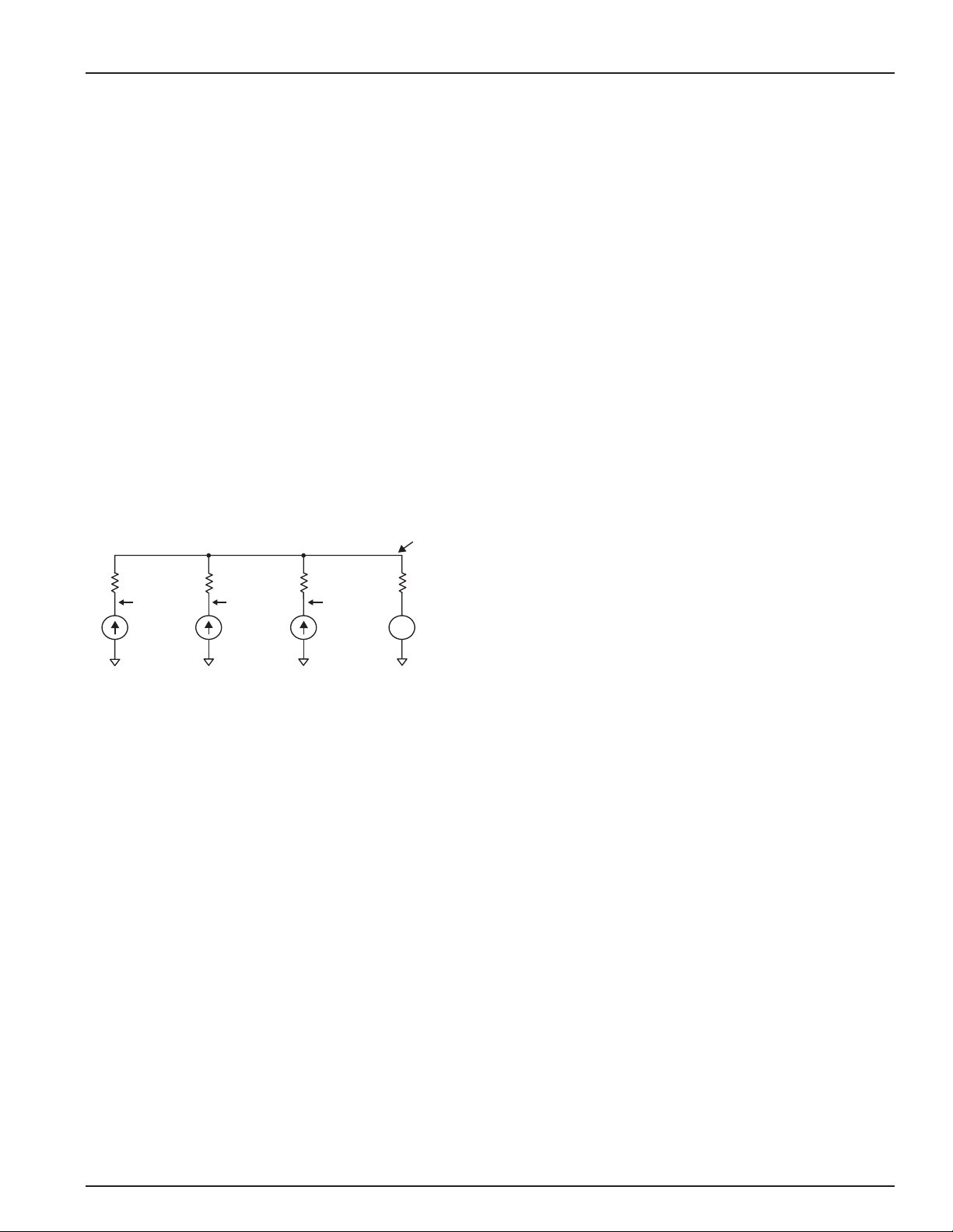
θca= 65°C/W for the KH231 without heat sink in still air.
30°C/W for the KH231 with a Wakefield 215 heat
sink in still air.
10°C/W for the KH231 with a Wakefield 215 heat
sink at 300 ft/min air.
30°C/W for the KH231 with a Thermalloy 2240A
heat sink in still air.
5°C/W for the KH231 with a Thermalloy 2240A
heat sink at 500 ft/min air.
For example, with the KH231 operating at ±15V while
driving a 100Ω load at 15Vppoutput (50% duty cycle
pulse waveform, DC = 0), P
(npn)
= P
(pnp)
= 190mW (R
col
= 33) and P
(cir)
= 0.48W. Then with the Wakefield
215 heat sink and air flow of 300 ft/min the output
transistors’ Tjis 28°C above ambient and worst case Tjin
the rest of the circuit is 32°C above ambient. In still air,
however, the rise in Tjis 45°C and 49°C, respectively.
With no heat sink, the rise in Tjis 75°C and 79°C,
respectively! Under most conditions, HEAT SINKING IS
REQUIRED.
Other methods of heat sinking may be used, but for
best results, make contact with the base of the KH231
package, use a large thermal capacity heat sink and use
forced air convection.
Low VCCOperation: Supply Current Adjustment
The KH231 is designed to operate on supplies as low as
±5V. In order to improve full bandwidth at reduced supply voltages, the supply current (ICC) must be increased.
The plot of Bandwidth vs. VCC, shows the effect of shorting pins 1 and 2 and pins 8 and 9; this will increase both
bandwidth and supply current. Care should be taken to
not exceed the maximum junction temperatures; for this
reason this technique should not be used with supplies
exceeding ±10V. For intermediate values of VCC,
external resistors between pins 1 and 2 and pins 8 and 9
can be used.
Offset Voltage Adjustment
If trimming of the input offset voltage (Vos= Vni-Vin) is
desired, a resistor value of 10kΩ to 1MΩ placed between
pins 8 and 9 will cause Vosto become more negative by
8mV to 0.2mV respectively. Similarly, a resistor placed
between pins 1 and 2 will cause Vos, to become more
positive.
Thermal Considerations
At high ambient temperatures or large internal power
dissipations, heat sinking is required to maintain
acceptable junction temperatures. Use the thermal
model on the previous page to determine junction
temperatures. Many styles of heat sinks are available for
TO-8 packages; the Thermalloy 2240 and 2268 are good
examples. Some heat sinks are the radial fin type which
cover the pc board and may interfere with external
components. An excellent solution to this problem is to
use surface mounted resistors and capacitors. They
have a very low profile and actually improve high
frequency performance. For use of these heat sinks with
conventional components, a 0.1”high spacer can be inserted
under the TO-8 package to allow sufficient clearance.
P
(circuit)
= (ICC)((+VCC) – (VCC)) where ICC= 16mA at ±15V
P
(xxx)
= [(±VCC) – V
out
– (I
col
) (R
col
+ 4)] (I
col
) (%Duty)
For positive Voand VCC, this is the power in the npn
device. For negative Voand VCC, this is the power in the
pnp device.
I
col
= Vo/RLor 4mA, whichever is greater. (Include feed-
back R in RL.)
R
col
is a resistor (33Ω recommended) between the xxx
collector and ±VCC.
The limiting factor for output current and voltage is junction
temperature. Of secondary importance is I
(out)
, which
should not exceed 150mA.
T
j(pnp)
= P
(pnp)
(100 + θca) + (P
(cir)
+ P
(npn)
)(θca) + Ta,
similar for T
j(npn)
.
T
j(cir)
= P
(cir)
(48 + θca) + (P
(pnp)
+ P
(npn)
)(θca) + Ta.
T
case
100°C/W
T
j(pnp)
P
pnp
100°C/W
T
j(npn)
P
npn
17.5°C/W
T
j(circuit)
P
circuit
+
-
θ
ca
T
ambient
Page 6
DISCLAIMER
FAIRCHILD SEMICONDUCTOR RESERVES THE RIGHT TO MAKE CHANGES WITHOUT FURTHER NOTICES TO ANY PRODUCTS HEREIN TO IMPROVE RELIABILITY, FUNCTION OR DESIGN. FAIRCHILD
DOES NOT ASSUME ANY LIABILITY ARISING OUT OF THE APPLICATION OR USE OF ANY PRODUCT OR CIRCUIT DESCRIBED HEREIN; NEITHER DOES IT CONVEY ANY LICENSE UNDER ITS PATENT
RIGHTS, NOR THE RIGHTS OF OTHERS.
LIFE SUPPORT POLICY
FAIRCHILD’S PRODUCTS ARE NOT AUTHORIZED FOR USE AS CRITICAL COMPONENTS IN LIFE SUPPORT DEVICES OR SYSTEMS WITHOUT THE EXPRESS WRITTEN APPROVAL OF THE PRESIDENT
OF FAIRCHILD SEMICONDUCTOR CORPORATION. As used herein:
1. Life support devices or systems are devices or systems which, (a) are intended for
surgical implant into the body, or (b) support or sustain life, and (c) whose failure to
perform when properly used in accordance with instructions for use provided in the
labeling, can be reasonably expected to result in a significant injury of the user.
2. A critical component in any component of a life support device or system whose
failure to perform can be reasonably expected to cause the failure of the life
support device or system, or to affect its safety or effectiveness.
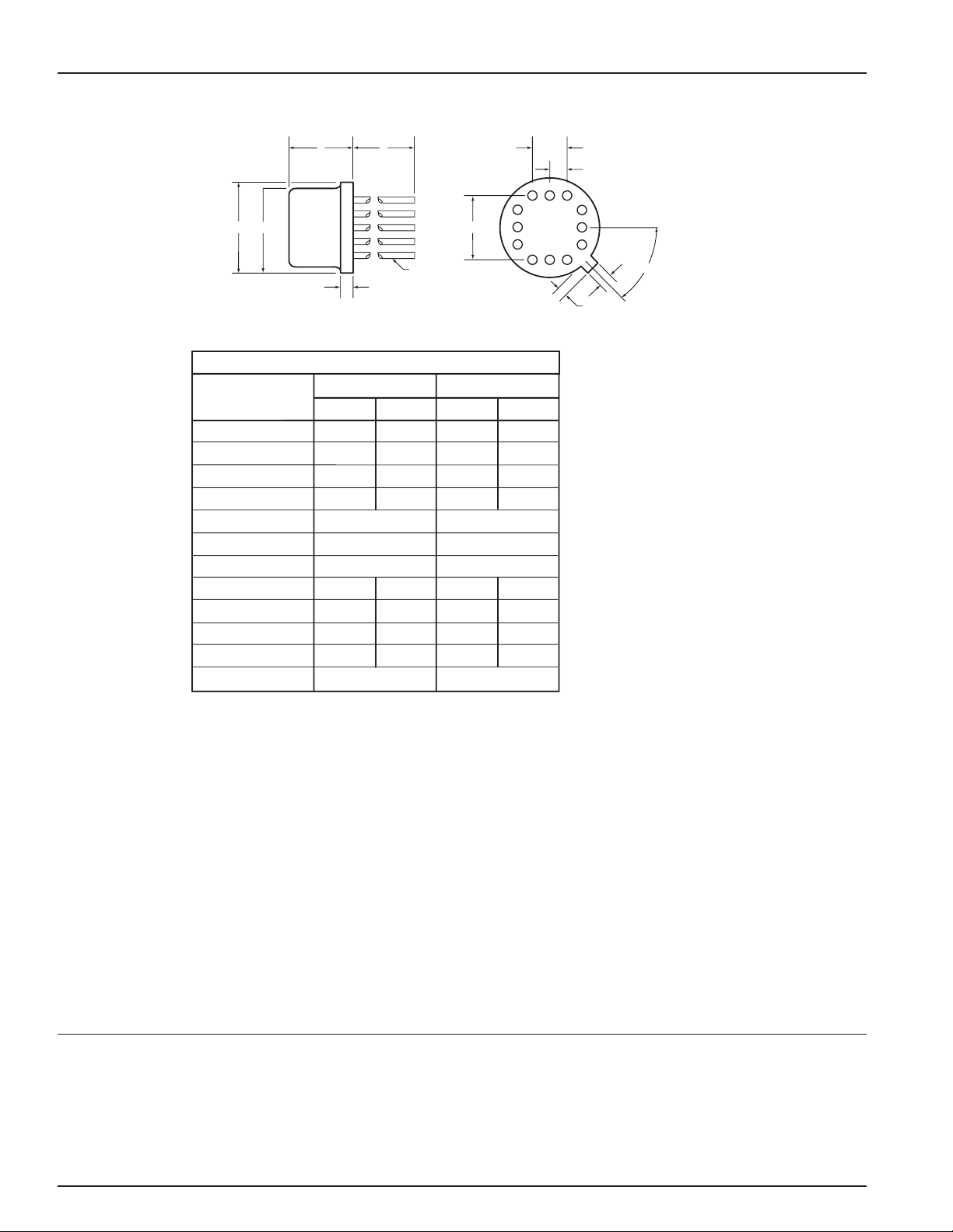
KH231 Package Dimensions
DATA SHEET KH231
www.fairchildsemi.com © 2001 Fairchild Semiconductor Corporation
L
e
φb
φDD
A
1
F
TO-8
SYMBOL
A 0.142 0.181 3.61 4.60
φb 0.016 0.019 0.41 0.48
φD 0.595 0.605 15.11 15.37
φD
1
e 0.400 BSC 10.16 BSC
e
1
e
2
F 0.016 0.030 0.41 0.76
k 0.026 0.036 0.66 0.91
k
1
L 0.310 0.340 7.87 8.64
α 45° BSC 45° BSC
INCHES MILIMETERS
Minimun Maximum Minimum Maximum
0.543 0.555 13.79 14.10
0.200 BSC 5.08 BSC
0.100 BSC 2.54 BSC
0.026 0.036 0.66 0.91
e
1
e
2
9
87
6
10
5
11
4
12
k
1
23
k
1
NOTES:
α
Seal: cap weld
Lead finish: gold per MIL-M-38510
Package composition:
Package: metal
Lid: Type A per MIL-M-38510
 Loading...