

Page 1
E2Q0030-38-72
This version: Jul. 1998
Previous version: Jan. 1998
KGF1323¡ electronic components
¡ electronic components
KGF1323
Power FET(Plastic Package Type)
GENERAL DESCRIPTION
The KGF1323, housed in a SOT-89 type plastic-mold package, is a discrete UHF-band power FET
that features high efficiency and high output power. The KGF1323 specifications are guaranteed
to a fixed matching circuit for 5.8 V and 850 MHz; external impedance-matching circuits are also
required. Because of its high efficiency, high output power (more than 33 dBm), and plastic
package, the KGF1323 is ideal as a transmitter-final-stage amplifier for personal handy phones,
such as TDMA-type cellular phones.
FEATURES
• High output power: 33 dBm (min.)
• High efficiency: 70% (typ.)
• Low thermal resistance: 23°C/W (typ.)
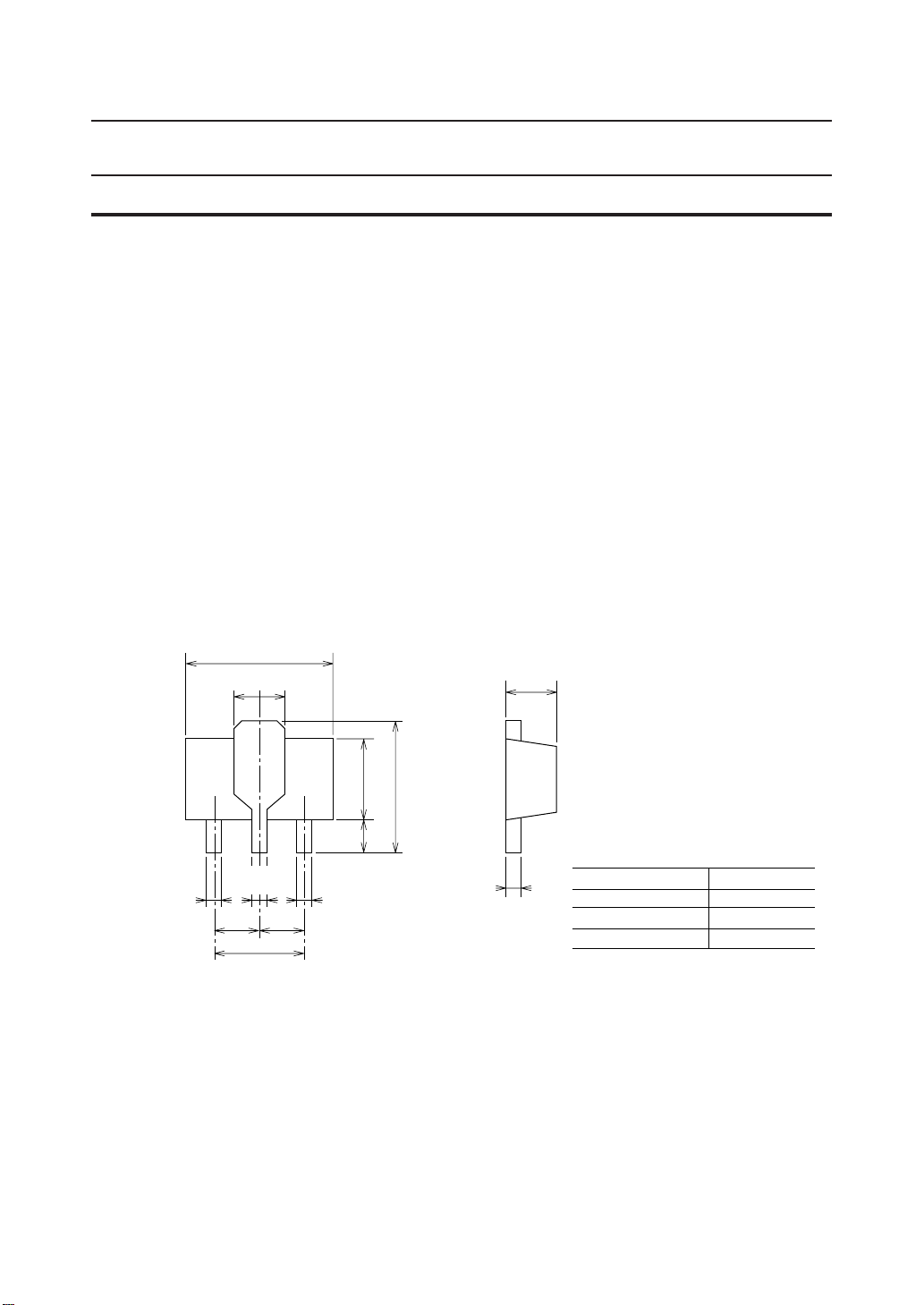
• Package: 3PMMP (SOT-89 type)
PACKAGE DIMENSIONS
4.5±0.1
+0.15
1.6
–0.10
+0.08
0.48
–0.05
3±0.1
0.4
+0.08
–0.05
1.5±0.1 1.5±0.1
0.4
+0.08
–0.05
0.11
±
2.5
0.2
±
0.2
±
4
±
0.05
0.39
(Unit: mm)
1.5±0.1
Package material
Lead frame material
Pin treatment
Solder plate thickness
Epoxy resin
Cu
Solder plating
5 mm or more
1/7
Page 2
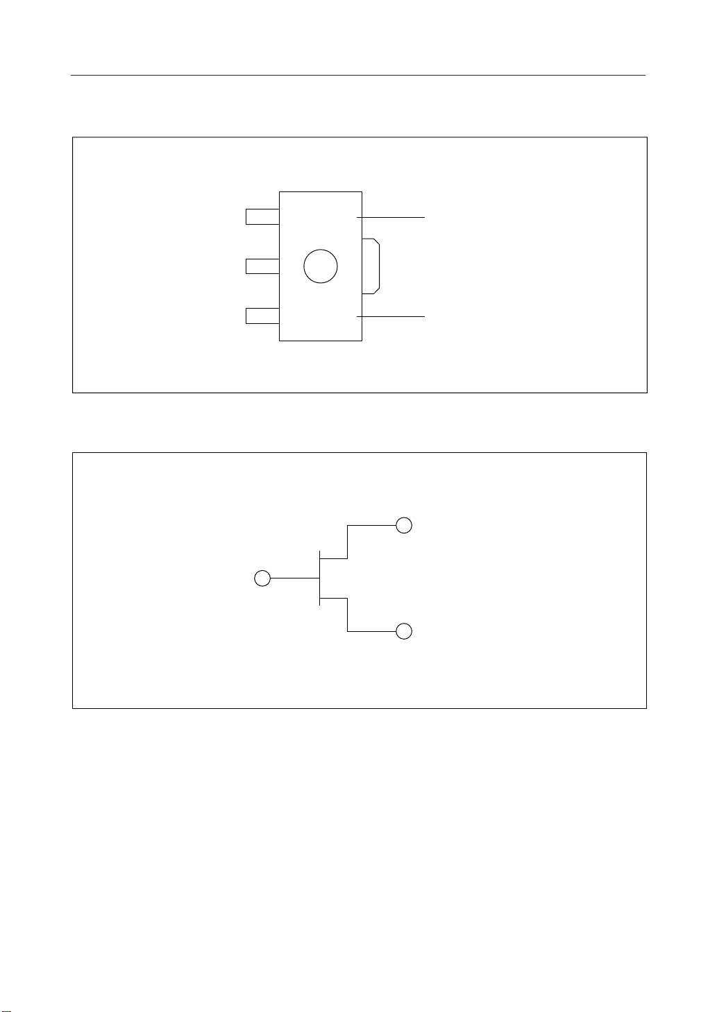
MARKING
KGF1323¡ electronic components
CIRCUIT
(1)
(2)
(3)
Gate(1)
P2
XX
PRODUCT TYPE
LOT NUMBER
(NUMERICAL or
ALPHABETICAL)
Drain(3)
(1) Gate
(2) Source
(3) Drain
Source(2)
2/7
Page 3
ABSOLUTE MAXIMUM RATINGS
KGF1323¡ electronic components
Item
Drain-source voltage
Gate-source voltage
Drain current I
Total power dissipation
Channel temperature
Storage temperature T
Symbol Condition Max.Unit
V
DS
V
GS
DS
P
tot
T
ch
stg
Ta = 25°C
Ta = 25°C
V
V
Ta = 25°C 3.0A —
Ta = Tc = 25°C
—
W
°C
— 125°C
Min.
—
–6.0
—
—
–45
ELECTRICAL CHARACTERISTICS
Item
Gate-source leakage current 100mA—VGS = –6 V —
Gate-drain leakage current 500mA—VGD = –16 V —
Drain-source leakage current 1500mA—VDS = 10 V, VGS = –6 V —
Drain current —A 2.0VDS = 1.5 V, VGS = 0 V —
Gate-source cut-off voltage –2.8V –3.8VDS = 3 V, IDS = 4.8 mA —
Output power —dBm
Linear gain G
Thermal resistance R
*1 Condition: f = 850 MHz, V
Symbol Condition Max.Unit
I
GSS
I
GDO
I
DS(off)
I
DSS
V
GS(off)
P
O
D
LIN
th
= 5.8 V, I
DS
(*1), P
(*1), P
= 22 dBm
IN
= 22 dBm %
IN
= 0 dBm
IN
= 240 mA
DSQ
dB
°C/W ——14Channel to case
Min.
33.0
60
Typ.
33.5
70Drain efficiency h
10
0.4
5
150
(Ta = 25°C)
—
—— 15.0(*1), P
3/7
Page 4

RF CHARACTERISTICS
KGF1323¡ electronic components
4/7
Page 5

Typical S Parameters
Freq(MHz)
1000.0
1100.0
1200.0
1300.0
1400.0
1500.0
1600.0
1700.0
1800.0
1900.0
2000.0
2100.0
2200.0
2300.0
2400.0
2500.0
2600.0
2700.0
2800.0
2900.0
3000.0
MAG(S11) ANG(S11) MAG(S21) ANG(S21) MAG(S12) ANG(S12) MAG(S22) ANG(S22)
500.0
600.0
700.0
800.0
900.0
0.921
0.921
0.920
0.917
0.917
0.914
0.913
0.911
0.909
0.907
0.903
0.901
0.899
0.893
0.892
0.888
0.885
0.881
0.875
0.873
0.869
0.866
0.863
0.856
0.854
0.852
–154.27
–160.15
–164.62
–168.17
–171.22
–173.90
–176.22
–178.42
179.67
177.63
175.71
173.93
172.15
170.52
169.01
167.01
165.66
163.90
162.38
160.75
159.09
157.56
155.95
154.35
152.84
151.31
3.891
3.291
2.854
2.519
2.250
2.041
1.871
1.721
1.599
1.491
1.404
1.324
1.248
1.188
1.127
1.077
1.027
0.983
0.944
0.906
0.876
0.844
0.816
0.789
0.756
0.736
91.63
87.28
82.96
79.31
76.01
72.42
69.42
66.28
63.39
60.39
57.29
54.72
51.47
48.90
45.99
43.37
40.36
37.89
35.01
32.96
29.90
27.58
24.58
22.20
19.48
17.09
V
0.037
0.038
0.039
0.040
0.040
0.041
0.042
0.043
0.044
0.045
0.046
0.047
0.048
0.048
0.050
0.051
0.052
0.053
0.055
0.055
0.057
0.058
0.060
0.061
0.063
0.063
= 5.8 V, V
DS
20.87
19.65
18.86
18.39
18.30
17.74
17.99
17.72
18.08
17.76
17.98
17.75
17.57
17.85
17.23
17.60
17.24
16.83
16.62
16.02
16.20
15.62
14.77
14.20
12.48
11.90
= –2.80 V, I
GS
0.655
0.657
0.659
0.661
0.660
0.661
0.660
0.660
0.660
0.661
0.658
0.660
0.654
0.660
0.653
0.658
0.651
0.655
0.650
0.652
0.649
0.649
0.649
0.646
0.649
0.646
KGF1323¡ electronic components
= 240 mA
DS
–176.53
–178.18
–179.48
179.28
178.41
177.38
176.61
175.52
174.76
173.75
172.81
171.94
170.90
170.04
169.08
168.02
167.14
165.92
164.99
163.98
162.58
161.68
160.24
159.52
158.10
157.17
5/7
Page 6

Typical S Parameters
V
DS
= 5.8 V, V
= –2.80 V, I
GS
Frequency : 0.5 to 3.0 GHz
Z0 = 50 W
= 240 mA
DS
KGF1323¡ electronic components
6/7
Page 7

Test Circuit and Bias Configuration for KGF1323 at 850 MHz
KGF1323¡ electronic components
C
V
GS
F
RFC
C
B
T
T
1
(1)
2
(3)
C
B
T
3
IN
C
C
C
C
1
2
(2)
C
C
F
V
DS
RFC
T
4
OUT
C
C
C
3
4
f = 850 MHz
T
: Z0 = 50 W, E = 28.5 deg
1
T
: Z0 = 50 W, E = 16.5 deg
2
C
= 2.0 pF, C2 = 10.0 pF, C3 = 5.0 pF, C4 = 1.0 pF
1
C
= 1000 pF, CF = 1000 pF, CB = 1000 pF, RFC = 200 nH
C
T3: Z0 = 50 W, E = 15.0 deg
T
: Z0 = 50 W, E = 30.0 deg
4
7/7
 Loading...