

Page 1
E2Q0025-38-71
This version: Jul. 1998
Previous version: Jan. 1998
KGF1262¡ electronic components
¡ electronic components
KGF1262
Medium-Power Amplifier
GENERAL DESCRIPTION
The KGF1262 is a medium-power amplifier, with frequencies ranging from the UHF-band to the
L-band, that features high gain, high output power, and low current operation. The KGF1262
specifications are guaranteed to a fixed matching circuit for 5.2 V and 1.9 GHz; external
impedance-matching circuits are also required. Because of the high gain and high output power
at the low operating current, the KGF1262 is ideal as a transmitter-driver amplifier for personal
handy phones of more than 1.5 GHz band.
FEATURES
• High linear gain: 15 dB (min.) at 1.9 GHz
• High output power: 18 dBm (min.) at 1.9 GHz
• Low current operation: 70 mA (max.)
• Self-bias circuit configuration with built-in source capacitor
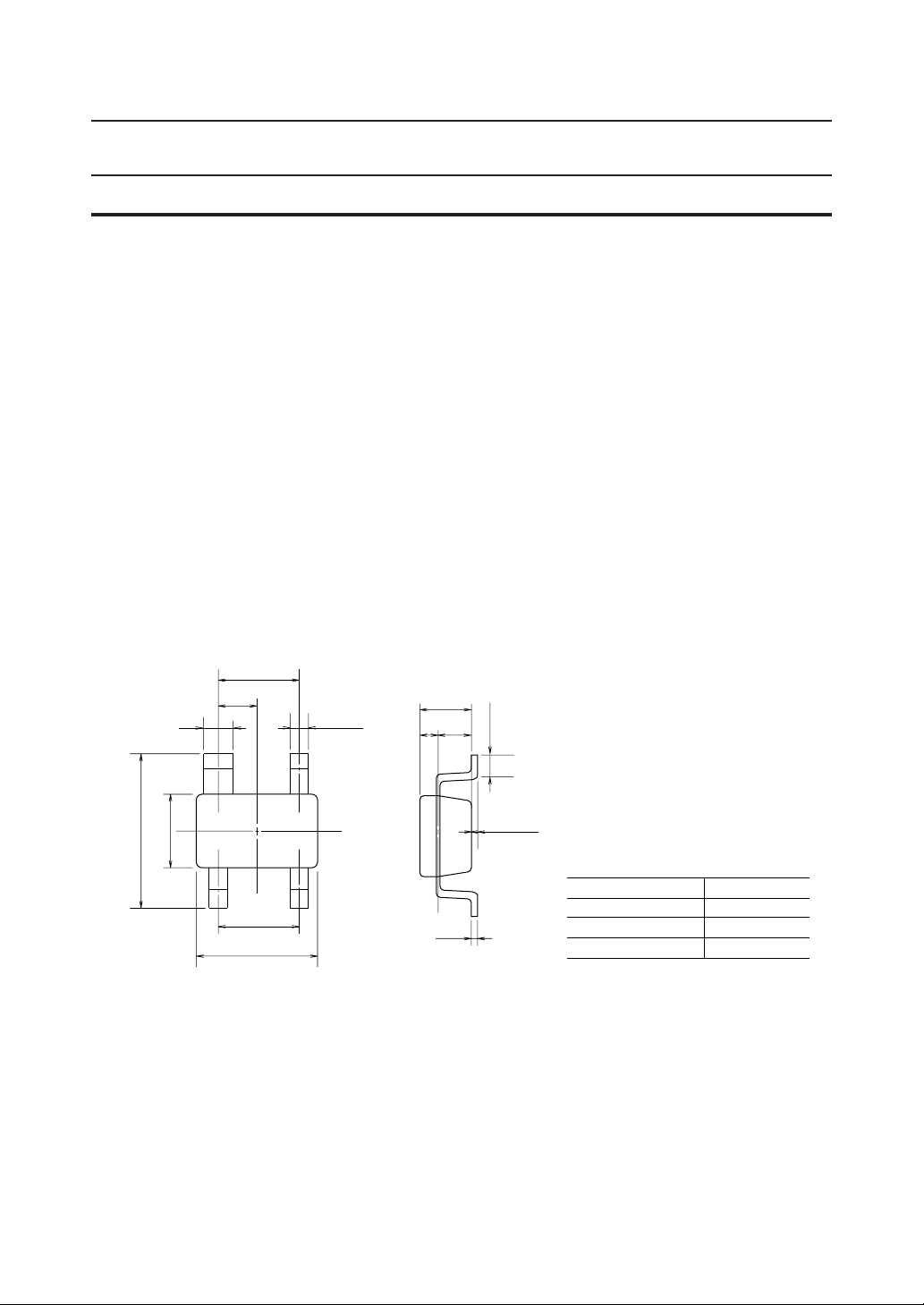
• package: 4PSOP
PACKAGE DIMENSIONS
1.8±0.1
0.85±0.05
+0.1
0.6
–0.05
3.0±0.2
1.5±0.15
1.9±0.1
2.8±0.15
0.4
+0.1
–0.05
1.1±0.15
0.36 0.74
+0.03
0.125
–0
(Unit: mm)
0.3 MIN
0 to 0.15
Package material
Lead frame material
Pin treatment
Solder plate thickness
Epoxy resin
42 alloy
Solder plating
5 mm or more
1/10
Page 2
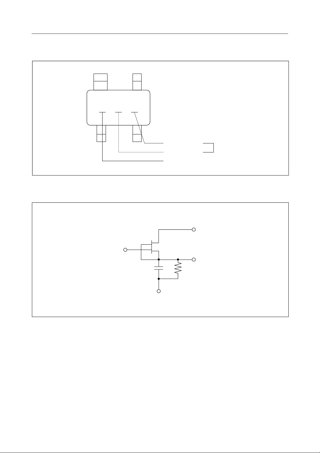
MARKING
(4) (3)
X
XN
KGF1262¡ electronic components
CIRCUIT
(1)
Gate(1)
(2)
NUMERICAL
ALPHABETICAL
PRODUCT TYPE
GND(4)
Drain(3)
Source(2)
LOT
NUMBER
(1) Gate
(2) Source
(3) Drain
(4) GND
2/10
Page 3
ABSOLUTE MAXIMUM RATINGS
KGF1262¡ electronic components
Item
Drain-source voltage
Gate-source voltage
Drain current I
Total power dissipation
Channel temperature
Storage temperature T
Symbol Condition Max.Unit
V
DS
V
GS
DS
P
tot
T
ch
stg
Ta = 25°C
Ta = 25°C
V
V
Ta = 25°C 360mA —
Ta = 25°C
—
mW
°C
— 125°C
Min.
—
–5.0
—
—
–45
10
0.4
300
150
ELECTRICAL CHARACTERISTICS
(Ta = 25°C)
Item
Gate-source leakage current 0.1mA —VGS = –5 V —
Gate-drain leakage current 0.5mA —VGD = –15 V —
Drain-source leakage current 1.0mA —VDS = 3 V, VGS = –2.5 V —
Drain current —mA 180VDS = 3 V, VGS = 0 V —
Operating current 70.0mA —(*1), P
Gate-source cut-off voltage –1.0mA –2.0VDS = 3 V, IDS = 720 mA—
Linear gain G
Output power —dBm
*1 Self-bias condition: V
Symbol Condition Max.Unit
I
GSS
I
GDO
I
DS(off)
I
DSS
I
D
V
GS(off)
m
LIN
P
O
= 5 V±0.25 V, V
DD
V
(*1), P
= 7 dBm 50.0
IN
= 3 V, IDS = 60 mA mS
DS
= –10 dBm
IN
= 7 dBm
IN
= 0 V, f = 1.9 GHz
G
dB
Min.
100
18.0
Typ.
—Transconductance g
20.0
—
—15.0 16.5(*1), P
3/10
Page 4

RF CHARACTERISTICS
KGF1262¡ electronic components
4/10
Page 5

KGF1262¡ electronic components
5/10
Page 6

Typical S Parameters
Freq(MHz)
1000.0
1100.0
1200.0
1300.0
1400.0
1500.0
1600.0
1700.0
1800.0
1900.0
2000.0
2100.0
2200.0
2300.0
2400.0
2500.0
2600.0
2700.0
2800.0
2900.0
3000.0
MAG(S11) ANG(S11) MAG(S21) ANG(S21) MAG(S12) ANG(S12) MAG(S22) ANG(S22)
500.0
600.0
700.0
800.0
900.0
0.861
0.885
0.938
0.969
0.972
0.942
0.907
0.852
0.804
0.756
0.718
0.681
0.654
0.631
0.618
0.603
0.594
0.585
0.581
0.582
0.578
0.581
0.587
0.592
0.597
0.611
–43.20
–46.52
–53.35
–62.62
–72.43
–82.27
–91.58
–99.25
–105.78
–112.04
–116.78
–121.54
–125.66
–129.73
–133.88
–137.40
–140.49
–143.89
–146.80
–150.18
–152.79
–156.41
–158.85
–161.90
–164.17
–167.83
8.314
7.319
7.176
7.448
7.617
7.566
7.454
7.080
6.706
6.346
6.004
5.672
5.394
5.093
4.889
4.659
4.501
4.321
4.179
4.056
3.902
3.786
3.685
3.578
3.502
3.398
132.26
131.88
131.57
127.57
121.79
113.36
105.56
97.79
91.46
85.32
79.92
74.96
70.48
65.90
61.24
57.66
53.61
50.05
46.29
42.23
38.65
35.05
31.84
27.91
25.03
20.74
0.023
0.032
0.035
0.038
0.041
0.037
0.038
0.037
0.038
0.038
0.040
0.046
0.052
0.057
0.064
0.074
0.083
0.095
0.107
0.117
0.128
0.143
0.156
0.171
0.185
0.202
KGF1262¡ electronic components
V
= 5 V, VG = 0 V, ID = 45.4 mA
DD
81.74
73.96
68.04
58.11
59.61
52.91
55.56
61.75
66.19
75.05
78.36
85.13
88.18
93.35
95.49
95.70
94.46
94.21
96.61
94.20
92.99
91.07
89.38
88.38
87.34
84.36
0.708
0.740
0.739
0.724
0.693
0.657
0.630
0.610
0.599
0.591
0.584
0.589
0.588
0.594
0.598
0.605
0.614
0.619
0.624
0.628
0.643
0.646
0.662
0.668
0.683
0.696
–20.18
–23.72
–29.36
–34.75
–39.17
–42.84
–44.99
–46.73
–48.16
–49.34
–51.27
–52.35
–54.02
–56.54
–59.04
–60.99
–63.71
–66.74
–69.08
–72.55
–76.40
–80.05
–83.66
–86.20
–91.62
–96.08
6/10
Page 7

Typical S Parameters
V
= 5 V, VG = 0 V, ID = 45.4 mA
DD
Frequency : 0.5 to 3.0 GHz
Z0 = 50 W
KGF1262¡ electronic components
7/10
Page 8

Typical S Parameters
Freq(MHz)
1000.0
1100.0
1200.0
1300.0
1400.0
1500.0
1600.0
1700.0
1800.0
1900.0
2000.0
2100.0
2200.0
2300.0
2400.0
2500.0
2600.0
2700.0
2800.0
2900.0
3000.0
MAG(S11) ANG(S11) MAG(S21) ANG(S21) MAG(S12) ANG(S12) MAG(S22) ANG(S22)
500.0
600.0
700.0
800.0
900.0
0.916
0.927
0.964
0.993
1.005
0.987
0.967
0.920
0.876
0.836
0.797
0.763
0.733
0.706
0.691
0.669
0.661
0.651
0.643
0.648
0.638
0.646
0.650
0.651
0.659
0.667
–43.51
–48.23
–54.71
–63.63
–72.69
–82.39
–91.73
–99.80
–107.04
–113.69
–119.30
–124.95
–129.64
–134.46
–139.12
–143.06
–146.80
–149.92
–153.50
–157.16
–160.05
–164.22
–167.02
–170.84
–173.51
–177.55
6.335
5.762
5.580
5.892
5.909
6.026
5.982
5.754
5.571
5.299
5.086
4.821
4.628
4.421
4.262
4.068
3.913
3.747
3.620
3.475
3.359
3.210
3.130
3.000
2.930
2.809
140.34
139.83
136.14
132.31
126.70
117.94
111.07
101.93
95.56
88.68
82.78
77.21
71.96
67.14
61.28
56.47
51.74
47.17
43.20
38.19
34.18
30.03
26.08
21.96
18.10
13.75
0.027
0.039
0.042
0.043
0.048
0.047
0.051
0.053
0.055
0.059
0.060
0.065
0.071
0.076
0.083
0.089
0.100
0.112
0.123
0.136
0.146
0.164
0.176
0.193
0.211
0.225
KGF1262¡ electronic components
V
= 3 V, VG = 0 V, ID = 48.5 mA
DD
98.55
83.96
75.40
69.15
69.44
65.48
67.55
67.95
70.09
72.60
73.94
76.41
78.66
80.42
84.73
83.56
83.44
83.94
86.10
84.08
84.76
81.24
80.05
78.05
76.90
74.08
0.457
0.498
0.502
0.515
0.483
0.493
0.477
0.490
0.495
0.498
0.501
0.507
0.514
0.524
0.540
0.562
0.562
0.576
0.578
0.579
0.598
0.591
0.618
0.607
0.634
0.638
–4.57
–8.99
–19.93
–24.18
–28.86
–33.12
–34.38
–39.74
–41.60
–45.70
–49.18
–52.17
–55.11
–58.04
–62.81
–66.89
–71.44
–76.90
–79.82
–85.80
–90.54
–96.30
–101.05
–104.47
–112.05
–117.04
8/10
Page 9

Typical S Parameters
V
= 3 V, VG = 0 V, ID = 48.5 mA
DD
Frequency : 0.5 to 3.0 GHz
Z0 = 50 W
KGF1262¡ electronic components
9/10
Page 10

Test Circuit and Bias Configuration for KGF1262 at 1.9 GHz
KGF1262¡ electronic components
IN
C
S
R
G
T
T
2
1
(2)
(1) (3)
KGF
T
5
1262
C
C
T
C
T
3
1
4
C
2
T1: Z0 = 75 W, E = 90 deg
T
: Z0 = 75 W, E = 55 deg
2
T
= T9: Z0 = 100 W, E = 1 deg
3
C
= 1.2 pF, C2 = 1.5 pF, C3 = 0.6 pF, C4 = 0.4 pF, CS = 100 pF
1
C
C(DC Block)
RFC = 60 nH, R
= 1000 pF, C
= 1000 W
G
(4)
B(By-pass)
T
9
T5: Z0 = 75 W, E = 70 deg
T
: Z0 = 75 W, E = 65 deg
6
T
= T7 = T8: Z0 = 100 W, E = 5 deg
4
= 1000 pF, C
F(Feed through)
C
B
T
6
RFC
C
F
V
DD
OUT
C
C
T
7
C
T
8
C
3
4
= 1000 pF
10/10
 Loading...