

Page 1
E2Q0022-38-71
This version: Jul. 1998
Previous version: Jan. 1998
KGF1183¡ electronic components
¡ electronic components
KGF1183
Medium-Power Amplifier
GENERAL DESCRIPTION
The KGF1183 is a two-stage medium-power UHF-band amplifier that features high gain and
high output power. The internally matched 50 W input eliminates external impedance-matching
circuits for the input, but it requires a simple matching circuit for the output. All specifications
for this device are guaranteed at 5 V and 850 MHz. Because of the high gain and high output
power, the KGF1183 is ideal as a transmitter-intermediate-stage amplifier for personal handy
phones.
FEATURES
• Internally matched 50 W input
• High linear gain: 20 dB (min.)
• High output power: 17 dBm (min.)
• Low current operation: 80 mA (max.)
• Self-bias circuit configuration with built-in source capacitor
• Package: 4PSOP
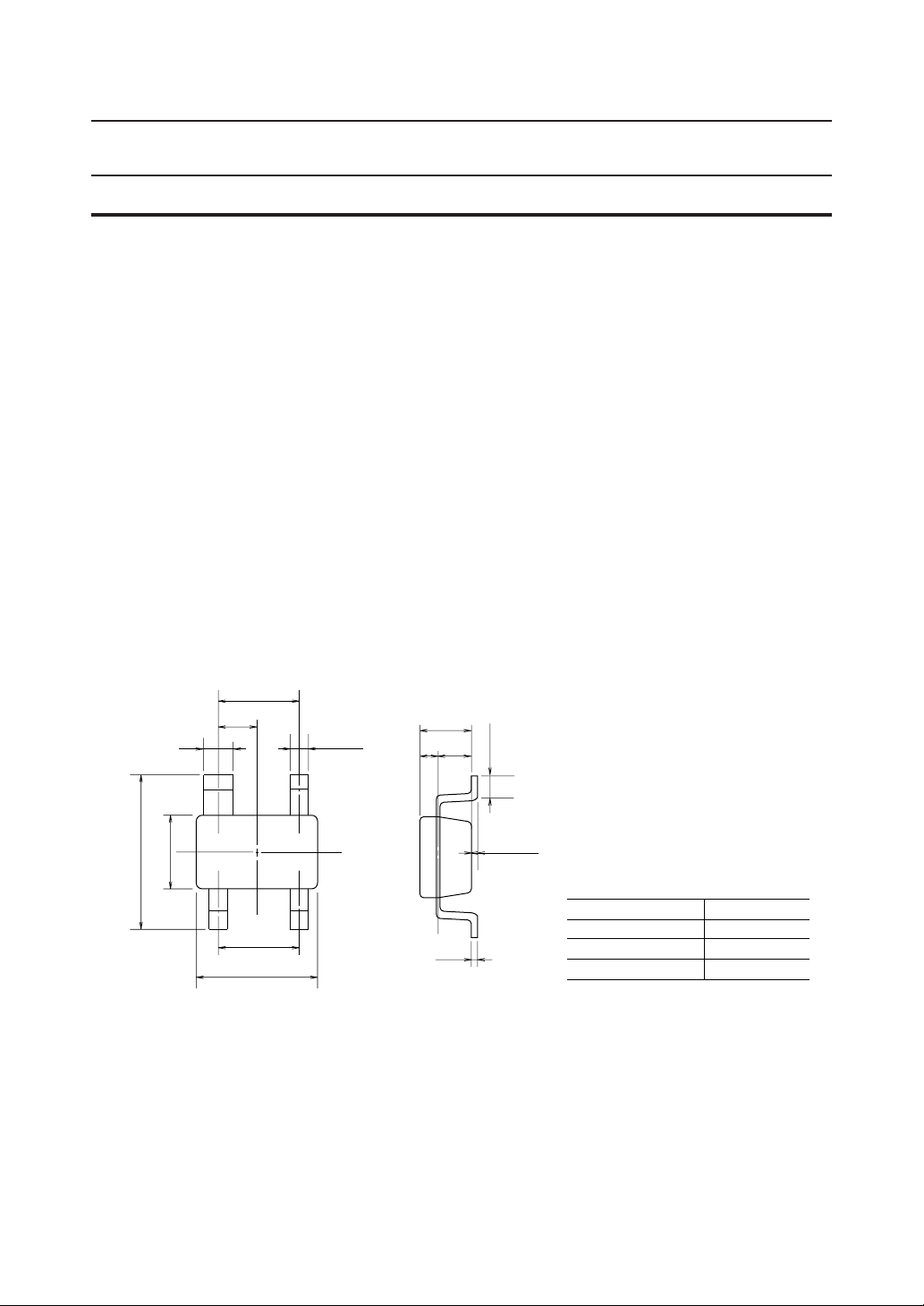
PACKAGE DIMENSIONS
1.8±0.1
0.85±0.05
+0.1
0.6
–0.05
3.0±0.2
1.5±0.15
1.9±0.1
2.8±0.15
0.4
+0.1
–0.05
1.1±0.15
0.36 0.74
+0.03
0.125
–0
(Unit: mm)
0.3 MIN
0 to 0.15
Package material
Lead frame material
Pin treatment
Solder plate thickness
Epoxy resin
42 alloy
Solder plating
5 mm or more
1/11
Page 2
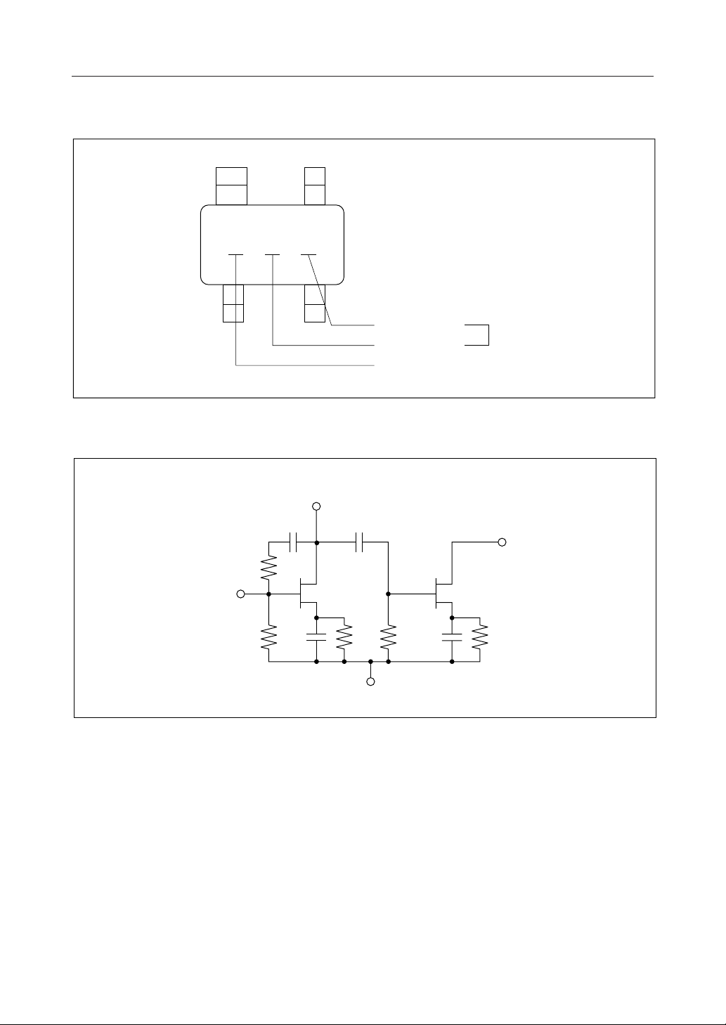
MARKING
(4) (3)
X
XC
KGF1183¡ electronic components
CIRCUIT
(1)
IN(1)
(2)
VD1(2)
C
f
R
f
Q
1
R
G1
C
S1
NUMERICAL
ALPHABETICAL
PRODUCT TYPE
C
C
R
S1
GND(4)
LOT
NUMBER
OUT(3)
Q
2
R
G2
C
S2
R
S2
(1) IN
(2) V
D1
(3) OUT
(4) GND
2/11
Page 3
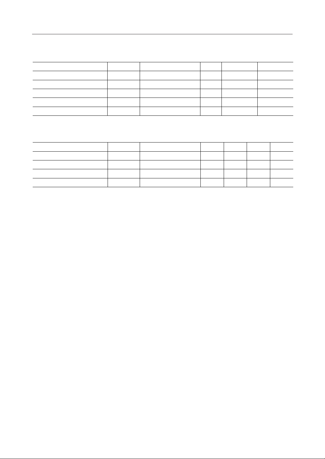
ABSOLUTE MAXIMUM RATINGS
KGF1183¡ electronic components
Item
Supply voltage
Input power
Total power dissipation
Channel temperature
Storage temperature T
Symbol Condition Max.Unit
V
DD
P
IN
P
tot
T
ch
stg
Ta = 25°C
Ta = 25°C
Ta = 25°C
—
— 125°C
ELECTRICAL CHARACTERISTICS
Item
Operating current 80.0mA
Linear gain G
Input return loss R
*1 Self-bias condition: V
Symbol Condition Max.Unit
I
D
O1
LIN
LIN
= 5.4 V, VG = 0 V, f = 850 MHz
DD
(*1), P
(*1), P
= 0 dBm
IN
= 0 dBm dBm
IN
= –20 dBm
IN
= –20 dBm
IN
V
dBm
mW
°C
dB
dB —— –9.0(*1), P
Min.
–45
Min.
—
17.0
—
—
—
—
Typ.
60.0
—Output power P
10
6
300
150
(Ta = 25°C)
—
—20.0 —(*1), P
3/11
Page 4
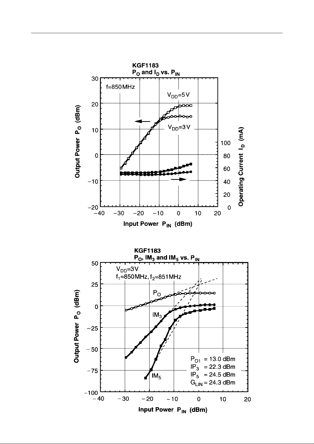
RF CHARACTERISTICS
KGF1183¡ electronic components
4/11
Page 5

KGF1183¡ electronic components
5/11
Page 6

KGF1183¡ electronic components
6/11
Page 7

Typical S Parameters
Freq(MHz)
1000.0
1100.0
1200.0
1300.0
1400.0
1500.0
1600.0
1700.0
1800.0
1900.0
2000.0
2100.0
2200.0
2300.0
2400.0
2500.0
2600.0
2700.0
2800.0
2900.0
3000.0
MAG(S11) ANG(S11) MAG(S21) ANG(S21) MAG(S12) ANG(S12) MAG(S22) ANG(S22)
500.0
600.0
700.0
800.0
900.0
0.314
0.322
0.343
0.383
0.423
0.444
0.452
0.434
0.412
0.391
0.378
0.358
0.345
0.337
0.329
0.326
0.316
0.314
0.306
0.304
0.306
0.306
0.299
0.305
0.306
0.309
–73.77
–92.04
–115.90
–145.41
–177.00
151.92
125.48
103.93
87.26
74.96
65.04
57.02
49.79
43.08
37.48
32.68
26.61
23.59
18.36
14.95
10.96
8.19
5.88
2.32
–0.50
–2.42
19.224
21.483
23.875
25.956
26.532
24.912
21.642
17.830
14.595
11.968
9.960
8.476
7.233
6.197
5.454
4.790
4.228
3.782
3.391
3.073
2.777
2.543
2.337
2.153
1.969
1.826
–23.89
–36.47
–51.66
–70.01
–90.60
–112.53
–132.14
–148.33
–160.93
–170.50
–179.14
173.73
167.79
162.18
157.26
152.77
148.19
143.78
139.98
136.45
133.45
129.56
126.43
123.33
120.37
117.03
0.018
0.024
0.030
0.041
0.049
0.056
0.059
0.057
0.054
0.058
0.055
0.056
0.060
0.058
0.063
0.063
0.065
0.065
0.071
0.071
0.072
0.079
0.082
0.080
0.089
0.090
103.91
106.42
104.25
95.92
84.93
71.59
64.47
59.02
56.85
55.96
51.34
53.89
50.50
51.85
53.39
52.40
49.90
52.61
52.15
53.77
54.15
54.77
47.98
51.00
49.99
52.10
KGF1183¡ electronic components
V
= 3 V, ID = 52.4 mA
DD
0.497
0.543
0.621
0.718
0.807
0.853
0.830
0.779
0.706
0.665
0.628
0.591
0.570
0.548
0.533
0.523
0.513
0.511
0.500
0.495
0.497
0.499
0.498
0.494
0.502
0.503
–89.19
–108.09
–129.90
–154.16
178.21
150.71
126.58
108.00
92.39
80.35
70.27
61.79
55.15
49.04
43.45
38.36
33.82
29.48
24.80
21.41
18.15
14.71
11.73
8.88
5.90
4.23
7/11
Page 8

Typical S Parameters
V
= 3 V, ID = 52.4 mA
DD
Frequency : 0.5 to 3.0 GHz
Z0 = 50 W
KGF1183¡ electronic components
8/11
Page 9

KGF1183¡ electronic components
Typical S Parameters
Freq(MHz)
1000.0
1100.0
1200.0
1300.0
1400.0
1500.0
1600.0
1700.0
1800.0
1900.0
2000.0
2100.0
2200.0
2300.0
2400.0
2500.0
2600.0
2700.0
2800.0
2900.0
3000.0
MAG(S11) ANG(S11) MAG(S21) ANG(S21) MAG(S12) ANG(S12) MAG(S22) ANG(S22)
500.0
600.0
700.0
800.0
900.0
0.311
0.316
0.329
0.357
0.388
0.400
0.400
0.382
0.358
0.344
0.331
0.316
0.308
0.301
0.296
0.291
0.286
0.283
0.276
0.276
0.277
0.278
0.272
0.274
0.283
0.281
–72.62
–91.07
–115.93
–146.89
179.78
147.73
120.80
100.26
85.18
72.14
62.96
55.47
48.64
42.07
37.46
32.35
27.68
22.88
18.39
15.62
12.64
9.04
6.80
3.45
0.55
–1.23
20.449
22.960
25.588
27.665
27.761
25.369
21.527
17.527
14.264
11.683
9.725
8.284
7.102
6.073
5.356
4.699
4.159
3.720
3.346
3.023
2.729
2.511
2.312
2.110
1.925
1.799
–24.73
–37.93
–54.09
–73.68
–95.44
–117.65
–136.72
–152.22
–163.95
–173.03
178.84
171.93
166.11
160.60
155.85
151.14
147.16
142.47
138.93
135.93
132.24
128.36
125.53
122.37
119.21
115.84
0.018
0.022
0.027
0.037
0.044
0.049
0.052
0.052
0.050
0.052
0.051
0.051
0.050
0.056
0.059
0.059
0.061
0.063
0.068
0.072
0.072
0.075
0.080
0.077
0.086
0.086
103.61
105.35
104.30
96.33
86.08
70.92
67.86
61.66
56.88
61.57
57.39
58.63
54.46
52.69
58.46
53.42
55.83
57.68
56.74
57.15
56.20
53.27
53.50
56.57
52.11
53.99
V
= 5 V, ID = 59.3 mA
DD
0.502
0.524
0.573
0.635
0.691
0.711
0.689
0.652
0.606
0.582
0.554
0.537
0.523
0.513
0.503
0.500
0.499
0.500
0.493
0.493
0.491
0.500
0.504
0.499
0.507
0.512
–78.78
–98.88
–122.75
–150.85
176.66
146.53
120.34
100.99
84.56
72.49
62.52
54.24
47.76
41.90
36.50
31.17
26.72
22.85
19.15
16.08
12.60
9.73
6.98
4.55
1.76
–0.19
9/11
Page 10

Typical S Parameters
V
= 5 V, ID = 59.3 mA
DD
Frequency : 0.5 to 3.0 GHz
Z0 = 50 W
KGF1183¡ electronic components
10/11
Page 11

Test Circuit and Bias Configuration for KGF1183
Feed through
Capacitor 1000 pF
KGF1183¡ electronic components
V
= 5 V
DD
1000 pF
IN OUT
DC Block
1000 pF
50 W Line Z0 = 80 W, E = 58 deg Line, f = 850 MHz
Test Circuit Board for KGF 1183
Choke Coil
200 nH
(1) (3)
(2)
KGF
1183
(4)
+
–
Choke Coil
60 nH
DC Block
1000 pF
10 mF
Substrate: Glass-epoxy resin
( 0.8 mmt, 18 mt Cu plated both side, er = 4.8 )
11/11
 Loading...