

Page 1
E2Q0011-38-71
This version: Jul. 1998
Previous version: Jan. 1998
KGF1146¡ electronic components
¡ electronic components
KGF1146
Small-Signal Amplifier
GENERAL DESCRIPTION
The KGF1146 is a two-stage small-signal UHF-band amplifier that features low current operation, high output power, and high isolation. The KGF1146 specifications are guaranteed to a fixed
matching circuit for 5 V and 850 MHz; external impedance-matching circuits are also required.
Because of the high isolation, the KGF1146 is an ideal part for a VCO-buffer amplifiers and an
intermediate-stage amplifier for personal handy phones, such as cellular phones.
FEATURES
• Low current operation: 2.5 mA (max.)
• High output power: 1.5 dBm (min.)
• High isolation: –40 dB
• Self-bias circuit configuration with built-in source capacitor
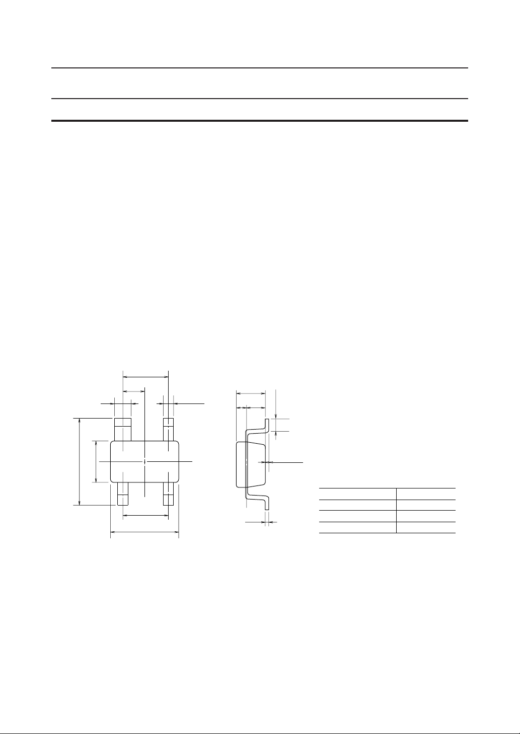
• Package: 4PSOP
PACKAGE DIMENSIONS
1.8±0.1
0.85±0.05
+0.1
0.6
–0.05
3.0±0.2
1.5±0.15
1.9±0.1
2.8±0.15
0.4
+0.1
–0.05
1.1±0.15
0.36 0.74
+0.03
0.125
–0
(Unit: mm)
0.3 MIN
0 to 0.15
Package material
Lead frame material
Pin treatment
Solder plate thickness
Epoxy resin
42 alloy
Solder plating
5 mm or more
1/7
Page 2
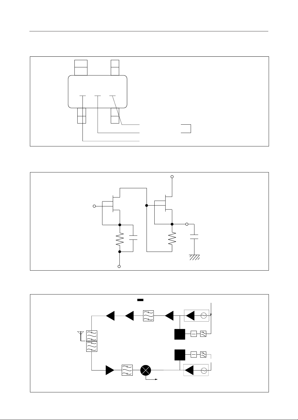
MARKING
(4) (3)
X
XB
KGF1146¡ electronic components
(1)
(2)
ALPHABETICAL
NUMERICAL
PRODUCT TYPE
CIRCUIT
D (3)
(1)
G
(4) GND
APPLICATION EXAMPLE FOR PORTABLE PHONES
S (2)
LOT
NUMBER
100 pF
(1) Gate
(2) Source
(3) Drain
(4) GND
Antenna
Duplexer
KGF1175
Head amplifier
KGF1305 KGF1254/56
SAW
filter
Driver
amplifler
amplifier
KGF1155
GaAs device
SAW
filter
amplifier
KGL2115
KGL2115
Mixer
Receiving
system
intermediate
frequency
KGF1165
Wide-band
amplifier
Prescaler
Prescaler
Transmission system
intermediate frequency
KGF1145/46
Buffer amplifier. OscillatorPower
Divider
1
n
Divider
1
n
Buffer amplifier. Oscillator
KGF1145/46
VCO
Filter
Filter
VCO
2/7
Page 3
KGF1146¡ electronic components
ABSOLUTE MAXIMUM RATINGS
Item Symbol Unit Min. Max.
Drain-source voltage
Gate-source voltage
Drain current
Total power dissipation
Channel temperature
Storage temperature
V
DS
V
GS
I
DS
Ptot
Tch
Tstg
ELECTRICAL CHARACTERISTICS
Item Symbol Condition Unit Min. Max.
Gate-source leakage current
Gate-drain leakage current
Drain-source leakage current
Drain current
Operating current
Gate-source cut-off voltage
Transconductance
Output power
Isolation
I
GSS
I
GDO
I
DS(off)
I
DSS
V
GS(off)
g
P
ISO
I
D
m
O
V
= –3 V
GS
= –6 V
V
GDO
= 3 V, VGS = –2.0 V
V
DS
= 3 V, VGS = 0 V
V
DS
(*1), P
V
V
(*1), P
(*1), P
= –10 dBm
IN
= 3 V, IDS = 120 mA
DS
= 3 V, IDS = 2.0 mA
DS
= –10 dBm
IN
= –10 dBm
IN
V
V
mA
mW
°C
°C
mA
mA
mA
mA
mA
V
mS
dBm
dB
—
–3
—
—
—
–45
—
—
—
15
—
–1.5
8
1.5
40
(Ta = 25°C)
6
0.4
60
200
150
125
(Ta = 25°C)
12
60
120
—
2.5
–0.5
—
—
—
*1 Self-bias condition: V
= 5.0 ± 0.25 V, V
DD
= 0 V, f = 850 MHz
G
3/7
Page 4

RF CHARACTERISTICS
KGF1146¡ electronic components
Po vs. P
IN
10
0
Po (dBm)
5
(mA)
4
D
I
3
–10
2
–20
Output Power
VDD = 4.75 V
1
Operating Current
f = 850 MHz
–30
–40
–30 –20 –10 0
Input Power
P
IN
(dBm)
0
4/7
Page 5

Typical S Parameters
Freq(MHz)
1000.0
1100.0
1200.0
1300.0
1400.0
1500.0
1600.0
1700.0
1800.0
1900.0
2000.0
2100.0
2200.0
2300.0
2400.0
2500.0
2600.0
2700.0
2800.0
2900.0
3000.0
MAG(S11) ANG(S11) MAG(S21) ANG(S21) MAG(S12) ANG(S12) MAG(S22) ANG(S22)
500.0
600.0
700.0
800.0
900.0
1.016
1.008
1.002
0.995
0.988
0.981
0.973
0.963
0.956
0.945
0.938
0.929
0.918
0.906
0.897
0.880
0.868
0.855
0.847
0.830
0.819
0.804
0.792
0.778
0.770
0.754
–13.78
–16.42
–19.14
–21.80
–24.38
–26.95
–29.64
–32.24
–34.90
–37.58
–40.39
–42.98
–46.03
–48.76
–51.64
–54.61
–57.75
–60.87
–63.86
–66.88
–69.77
–72.90
–76.11
–79.41
–82.77
–85.91
3.144
3.184
3.091
3.060
2.952
2.961
2.741
2.687
2.557
2.481
2.316
2.187
2.009
1.872
1.775
1.710
1.650
1.562
1.499
1.470
1.413
1.364
1.337
1.304
1.287
1.238
–53.83
–65.20
–76.19
–84.59 87.52
–92.88
–98.49
–105.75
–111.43
–117.29
–122.72
–129.37
–134.82
–140.24
–151.35
–155.91
–161.08
–166.40
–171.49
–176.27
179.50
176.86
174.40
169.45
164.51
159.93
155.02
0.002
0.002
0.001
0.002
0.003
0.002
0.001
0.002
0.001
0.001
0.001
0.001
0.002
0.001
0.003
0.003
0.005
0.007
0.008
0.009
0.013
0.014
0.016
0.019
0.024
0.028
91.21
72.13
88.37
75.89
69.05
51.70
89.09
31.04
96.43
138.33
124.06
–115.76
–129.25
–128.46
–121.98
–139.31
–126.58
–127.50
–139.94
–129.23
–134.15
–136.16
–140.71
–134.62
–137.56
KGF1146¡ electronic components
= 5 V, ID = 1.85 mA
V
DD
0.954
0.954
0.954
0.952
0.950
0.948
0.952
0.944
0.945
0.941
0.941
0.937
0.941
0.932
0.934
0.929
0.926
0.927
0.923
0.924
0.920
0.919
0.914
0.916
0.914
0.916
–7.09
–8.39
–9.92
–11.21
–12.84
–14.07
–15.34
–16.82
–18.09
–19.74
–20.90
–22.03
–23.52
–24.82
–26.27
–27.28
–28.67
–29.86
–30.90
–32.30
–33.42
–34.91
–35.62
–37.07
–37.84
–38.89
5/7
Page 6

Typical S Parameters
V
= 5 V, ID = 1.85 mA
DD
Frequency : 0.5 to 3.0 GHz
Z0 = 50 W
KGF1146¡ electronic components
j1.0
j0.5
j2.0
j0.2
S
3.0
S
11
3.0
0.0 0.2 0.5 1.0 2.0 5.0
90
135
45
j5.0
0.5
3.0
3.0
0
S
12
0.5
S
21
180
0.5
22
5.0 4.0 3.0 2.0 1.0 0.01 0.02 0.03 0.04 0.05
0.5
6/7
Page 7

Test Circuit
KGF1146¡ electronic components
L1L2L2L1
Cc
IN
W2
L1 = 20 mm
L2 = 8 mm
L3 = 10 mm
C1 and C2 are tuned to obtain maximum output power.
W1
L3
W1 = 1 mm
W2 = 3 mm
Cc = 1000 pF
C1
C1, C2: Trimmer Capacitor
(Murata Giga-Trimmer,
max. 4.5 pF)
C2
W1
L3
Cc
Substrate parameters
e
= 2.6
r
h = 1.6 mm
Cc
OUT
VdW2
7/7
 Loading...