

Page 1
MICROWAVE CORPORATION
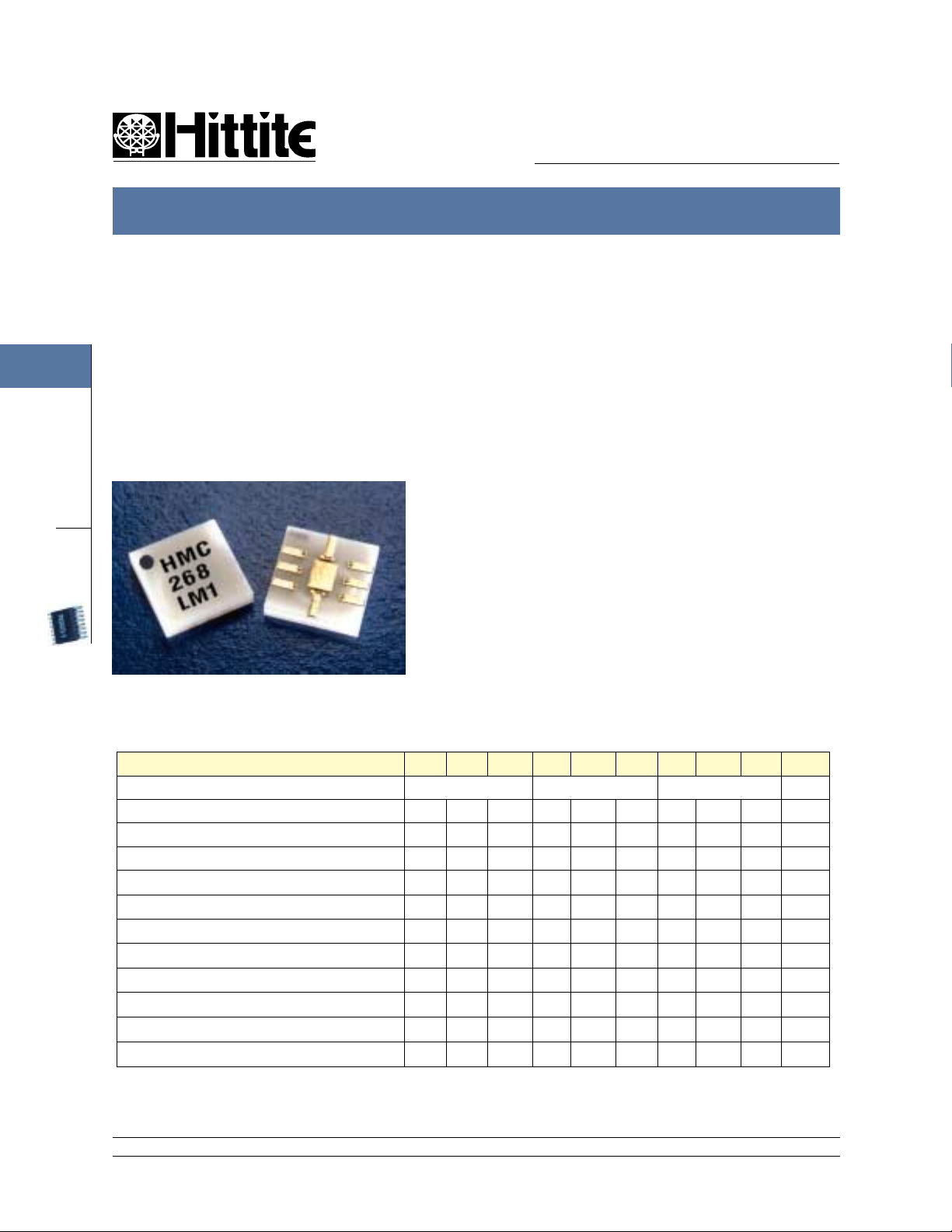
SMT LOW NOISE AMPLIFIER MMIC 20 - 32 GHz
HMC268LM1
FEBRUARY 2001
Features
SMT mmWAVE PACKAGE
1
EXCELLENT NOISE FIGURE : 2.6 dB
15 dB GAIN
P1 dB OUTPUT POWER: +13 dBm
AMPLIFIERS
SMT
V01.0900
General Description
The HMC268LM1 is a two stage GaAs MMIC Low
Noise Amplifier (LNA) in a SMT leadless chip
carrier package covering 20 to 32 GHz. The LM1
is a true surface mount broadband millimeterwave
package offering low loss & excellent I/O match,
preserving MMIC chip performance. Utilizing a
GaAs PHEMT process the device offers 2.6 dB
noise figure, 15 dB gain and +13 dBm output
power from a bias supply of +4V @ 45 mA. The
packaged LNA enables economical PCB SMT
assembly for millimeterwave point-to-point radios, LMDS, and SATCOM applications. As an
alternative to chip-and-wire hybrid assemblies
the HMC268LM1 eliminates the need for
wirebonding, thereby providing a consistent connection interface for the customer. All data is with
the non-hermetic, epoxy sealed LM1 packaged
LNA device mounted in a 50 ohm test fixture.
Guaranteed Performance, Vdd = +4V*, -55 to +85 deg C
retemaraP .niM .pyT .xaM .niM .pyT .xaM .niM .pyT .xaM stinU
**egnaRycneuqerF62-0203-6223-03zHG
niaG114171315181215181Bd
erugiFesioN5.22.36.24.38.28.3Bd
ssoLnruteRtupnI877Bd
ssoLnruteRtuptuO2187Bd
noitalosIesreveR623332823282Bd
)Bd1P(noisserpmoCBd1rofrewoPtuptuO711931931mBd
)tasP(rewoPtuptuOdetarutaS316141715181mBd
)3PI(tpecretnIredrOdrihTtuptuO312271225112mBd
)ddV(egatloVylppuS57.30.452.457.30.452.457.30.452.4cdV
)2ggV&1ggV(egatloVylppuS0.2-51.0-0.00.2-51.0-0.00.2-51.0-0.0cdV
)ddI(tnerruCylppuS540554055405Am
* Vdd = +4V, adjust Vgg1 & Vgg2 between -2.0 to 0.0 Vdc to achieve Idd = 45 mA.
** Acceptable gain and NF peformance is achievable down to 17 GHz.
12 Elizabeth Drive, Chelmsford, MA 01824 Phone: 978-250-3343 Fax: 978-250-3373 Web Site: www.hittite.com
1 - 28
Page 2
MICROWAVE CORPORATION
SMT LOW NOISE AMPLIFIER MMIC 20 - 32 GHz
HMC268LM1
V01.0900
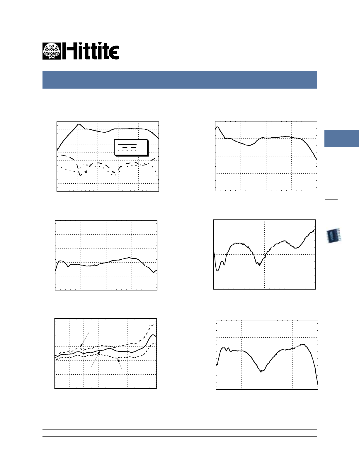
Broadband Gain and Return Loss
20
15
10
5
0
-5
-10
RESPONSE (dB)
-15
-20
-25
10 15 20 25 30 35
FREQUENCY (GHz)
S21
S11
S22
Isolation
0
-10
-20
-30
-40
REVERSE ISOLATION (dB)
FEBRUARY 2001
Gain
20
15
10
GAIN (dB)
5
0
15 20 25 30 35
FREQUENCY (GHz)
Input Return Loss
0
-5
-10
-15
INPUT R ETUR N L OSS (dB )
1
AMPLIFIERS
SMT
-50
15 20 25 30 35
FREQUENCY (GHz)
Noise Figure
5
4
3
2
NOISE FIGURE (dB)
1
0
20 22 24 26 28 30 32 34
+85 C
+25 C
FREQUENCY (GHz)
-40 C
-20
15 20 25 30 35
FREQUENCY (GHz)
Output Return Loss
0
-5
-10
-15
OUTPUT RETURN LOSS (dB)
-20
15 20 25 30 35
FREQUENCY (GHz)
12 Elizabeth Drive, Chelmsford, MA 01824 Phone: 978-250-3343 Fax: 978-250-3373 Web Site: www.hittite.com
1 - 29
Page 3
MICROWAVE CORPORATION
SMT LOW NOISE AMPLIFIER MMIC 20 - 32 GHz
HMC268LM1
FEBRUARY 2001
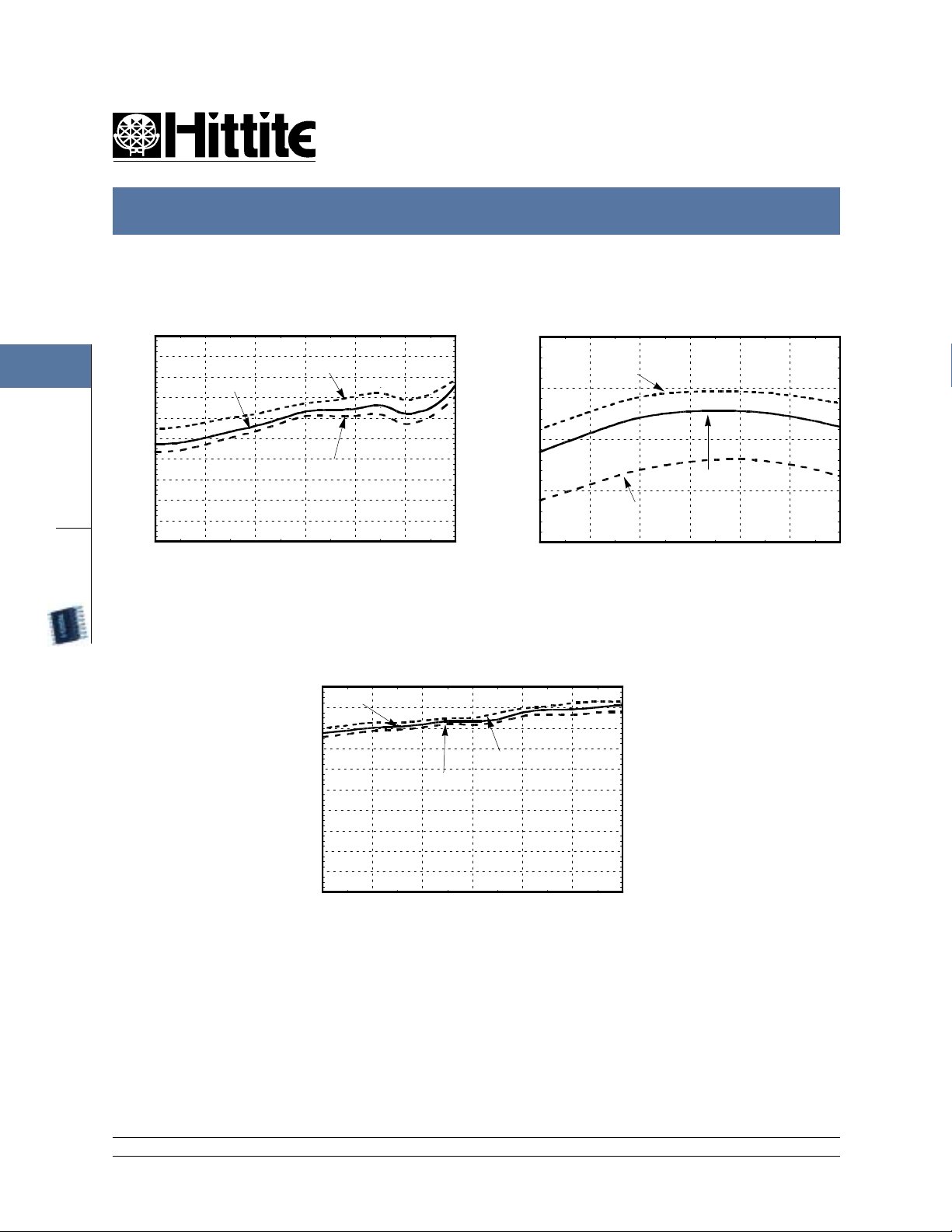
Output P1dB vs. Temperature
1
P1dB OUTPUT (dBm)
AMPLIFIERS
SMT
20
18
16
14
12
10
8
6
4
2
0
20 22 24 26 28 30 32
+25C
FREQUENCY (GHz)
-40C
+85C
Psat vs. Temperature
20
+25C
18
16
14
12
10
8
Psat (dBm)
6
4
2
0
20 22 24 26 28 30 32
Output IP3 vs. Temperature
THIRD ORDER INTERCEPT (dBm)
-40C
+85C
FREQUENCY (GHz)
V01.0900
30
-40C
25
20
+25C
15
+85C
10
20 22 24 26 28 30 32
FREQUENCY (GHz)
12 Elizabeth Drive, Chelmsford, MA 01824 Phone: 978-250-3343 Fax: 978-250-3373 Web Site: www.hittite.com
1 - 30
Page 4
MICROWAVE CORPORATION
SMT LOW NOISE AMPLIFIER MMIC 20 - 32 GHz
HMC268LM1
V01.0900
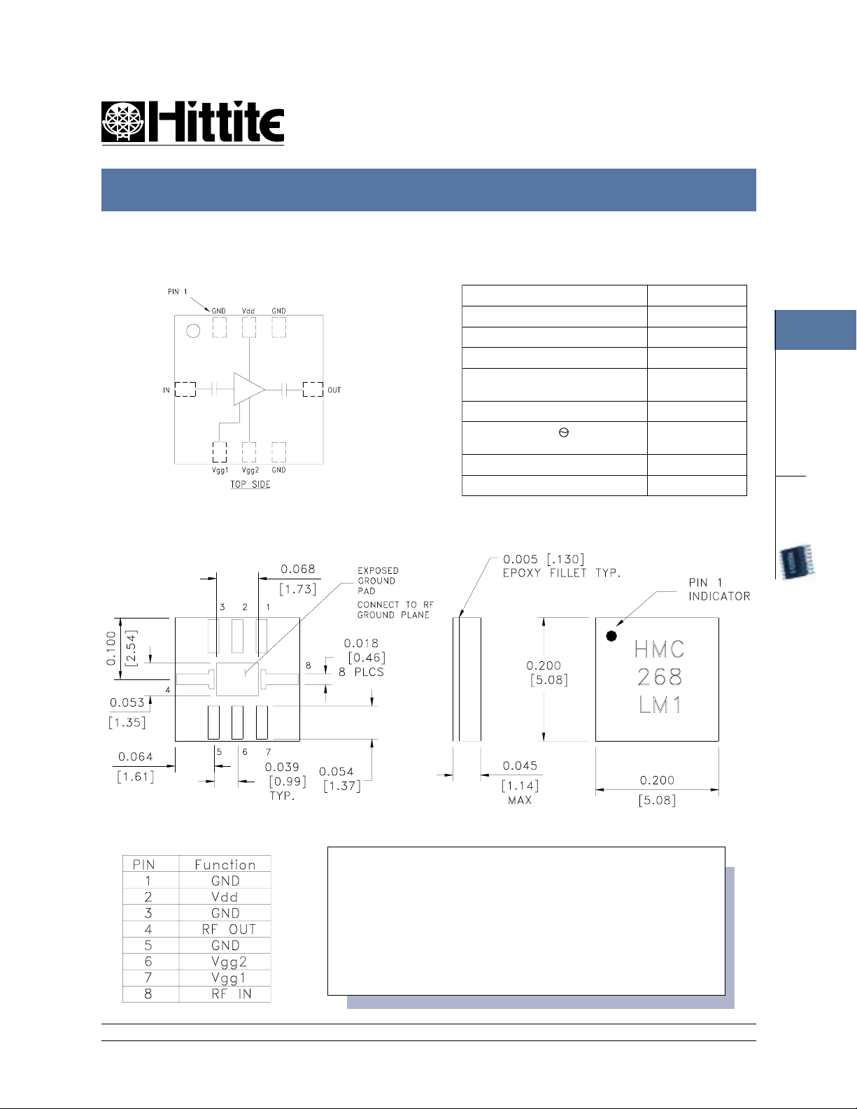
Functional Diagram
See HMC268LM1 Biasing Note Page 1 - 58
Outline
FEBRUARY 2001
Absolute Maximum Ratings
)ddV(egatloVylppuS
)ddI(tnerruCylppuSAm05
)2&1ggV(egatloVsaiBetaGcdV0.0ot0.2-
)2&1ggI(tnerruCetaGCDAm4
)niFR(rewoPtupnI
)ces1<deilpparewopFR,V4+=ddV(
)cT(erutarepmeTlennahC
)cj(ecnatsiseRlamrehT
)ediskcaBlennahC(
erutarepmeTegarotS051+ot56-
erutarepmeTgnitarepO58+ot55-
571oC
982oW/C
cdV5.4+
mBd51+
o
C
o
C
1
AMPLIFIERS
SMT
1. MATERIAL:
A) PACKAGE BODY & LID: PLASTIC.
B) PIN CONTACT : COPPER, 0.5 OUNCE.
2. PLATING : ELECTROLYTIC GOLD (20 TO 50 MICROINCHES TYPICAL) OVER
ELECTROLYTIC NICKEL (50 MICROINCHES MINIMUM).
3. DIMENSIONS ARE IN INCHES (MILLIMETERS).UNLESS OTHERWISE SPECIFIED
ALL TOLERANCES ARE ± 0.005 (± 0.13).
4. ALL GROUNDS MUST BE SOLDERED TO THE PCB RF GROUND.
5. SEE APPLICATION NOTE FOR RECOMMENDED ATTACHMENT TECHNIQUE TO PCB.
12 Elizabeth Drive, Chelmsford, MA 01824 Phone: 978-250-3343 Fax: 978-250-3373 Web Site: www.hittite.com
1 - 31
Page 5

MICROWAVE CORPORATION
SMT LOW NOISE AMPLIFIER MMIC 20 - 32 GHz
HMC268LM1
FEBRUARY 2001
HMC268LM1 Evaluation PCB
1
AMPLIFIERS
SMT
C2
C1
C1
C1
C2C2
LM1 Evaluation PCB
0.018
[0.46]
0.057
[1.45]
0.039
[0.99]
0.078
[1.98]
0.150
[3.81]
0.018
[0.46]
Suggested LM1 PCB Land Pattern
Tolerance: ±0.003" (±0.08 mm)
V01.0900
-B-
Suggested Ground Via Size:
Ø0.010" (0.25) and Qty: 8 to 12
-A-
0.053
[1.35]
ALL FEATURES
0.086
[2.18]
.003 A B
The grounded Co-Planar Wave Guide (G-CPW) PCB input/output transitions allow use of Ground-SignalGround (GSG) probes for testing. Suggested probe pitch is 400µm (16 mils). Alternatively, the board can
be mounted in a metal housing with 2.4 mm coaxial connectors.
Evaluation Circuit Board Layout Design Details
euqinhceTtuoyaLWPC-GotpirtSorciM
lairetaMuC,zo2/1htiw3004sregoR
ssenkcihTcirtceleiD)mm02.0("800.0
htdiWeniLpirtsorciM)mm64.0("810.0
htdiWeniLWPC-G)mm14.0("610.0
paGDNGoteniLWPC-G)mm31.0("500.0
remaiDeloHaiVdnuorG)mm31.0("800.0
1C.gkP2040,roticapaCFp001
2C
12 Elizabeth Drive, Chelmsford, MA 01824 Phone: 978-250-3343 Fax: 978-250-3373 Web Site: www.hittite.com
1 - 32
01
.gkP6021,roticapaCFp000,
LM1 Package Mounted to Evaluation PCB
Page 6

MICROWAVE CORPORATION
SMT LOW NOISE AMPLIFIER MMIC 20 - 32 GHz
HMC268LM1
V01.0900
FEBRUARY 2001
HMC268LM1 Recommended SMT Attachment Technique
Preparation & Handling of the LM1 Millimeterwave Package for Surface Mounting
The HMC LM1 package was designed to be compatible with
high volume surface mount PCB assembly processes. The
LM1 package requires a specific mounting pattern to allow
proper mechanical attachment and to optimize electrical
performance at millimeterwave frequencies. This PCB layout
pattern can be found on each LM1 product data sheet. It can
also be provided as an electronic drawing upon request from
Hittite Sales & Application Engineering.
Follow these precautions to avoid permanent damage:
Cleanliness: Observe proper handling procedures to ensure
clean devices and PCBs. LM1 devices should remain in their
original packaging until component placement to ensure no
contamination or damage to RF, DC & ground contact areas.
Static Sensitivity: Follow ESD precautions to protect against
ESD strikes ( see catalog page 8 - 2 ).
General Handling: Handle the LM1 package on the top with a
vacuum collet or along the edges with a sharp pair of bent
tweezers. Avoiding damaging the RF, DC, & ground contacts on the package bottom. Do not apply excess pressure
to the top of the lid.
Solder Materials & Temperature Profile: Follow the information contained in the application note. Hand soldering is
not recommended. Conductive epoxy attachment is not recommended.
Solder Paste
Solder paste should be selected based on the user’s experience and be compatible with the metallization systems
used. See the LM1 data sheet Outline drawing for pin & ground contact metallization schemes.
225
200
175
C)
0
150
125
100
TEMPERATURE (
75
50
25
012345678
Recommended solder reflow profile
for HMC LM1 SMT package
TIME (min)
1
AMPLIFIERS
SMT
Solder Paste Application
Solder paste is generally applied to the PCB using either a stencil printer or dot placement. The volume of solder
paste will be dependent on PCB and component layout and should be controlled to ensure consistent mechanical
& electrical performance. Excess solder may create unwanted electrical parasitics at high frequencies.
Solder Reflow
The soldering process is usually accomplished in a reflow oven but may also use a vapor phase process. A solder
reflow profile is suggested above.
Prior to reflowing product, temperature profiles should be measured using the same mass as the actual assemblies.
The thermocouple should be moved to various positions on the board to account for edge and corner effects and
varying component masses. The final profile should be determined by mounting the thermocouple to the PCB at the
location of the device.
Follow solder paste and oven vendor’s recommendations when developing a solder reflow profile. A standard
profile will have a steady ramp up from room temperature to the pre-heat temperature to avoid damage due to
thermal shock. Allow enough time between reaching pre-heat temperature and reflow for the solvent in the paste to
evaporate and the flux to completely activate. Reflow must then occur prior to the flux being completely driven off.
The duration of peak reflow temperature should not exceed 15 seconds. Packages have been qualified to withstand a peak temperature of 235°C for 15 seconds. Verify that the profile will not expose device to temperatures in
excess of 235°C.
Cleaning
A water-based flux wash may be used.
12 Elizabeth Drive, Chelmsford, MA 01824 Phone: 978-250-3343 Fax: 978-250-3373 Web Site: www.hittite.com
1 - 33
Page 7

MICROWAVE CORPORATION
SMT LOW NOISE AMPLIFIER MMIC 20 - 32 GHz
HMC268LM1
FEBRUARY 2001
HMC268LM1 General Biasing & Application Circuit
Optimal biasing of the HMC268LM1 SMT two stage low noise amplifier Vdd, Vgg1 & Vgg2 DC ports is
1
described below. The LNA schematic is repeated below. Note the recommended addition of the external
bypass chip capacitor. For additional general MMIC amplifier biasing guidance, please refer to the Hittite
Microwave “MMIC Amplifier Biasing Procedure” found on page 8-8 in our February 2000 catalog or on
www.hittite.com under the Application Note section.
AMPLIFIERS
SMT
RF IN
(PIN 8)
C1 C2
V 1
gg
(Pin 7)
(Pin 2)
Vdd
C1
50 W
Vds1
C1 C2
V 2
gg
(Pin 6)
Vds2
C2
25 W
RF OUT
(PIN 4)
V01.0900
seulaVtnenopmoCdednemmoceR
1CFp001
2CFp000,01
IMPORTANT DC LIMITS! When biasing the HMC268LM1 please note the following;
A) Do Not exceed 3.5 Vdc on internal circuit nodes Vds1 and Vds2 (internal Drain to Source volt-
ages). Calculate the Vds1&2 voltages from the LNA schematic above.
B) Do Not bias Vdd, Vgg1 & Vgg2 DC ports in such a way that Vgs becomes a positive voltage
(internal Gate to Source voltage).
HMC268LM1 Biasing Schemes for Performance Trade-Offs
The biasing may be adjusted slightly to achieve either low noise with lowest DC power consumption or low
noise with highest output power. Be sure to adhere to the IMPORTANT DC LIMITS! above while optimiz-
ing performance.
A) Low Noise and Low Power Consumption : Vdd = 3.5Vdc @ Idd = 30mA. Set Vgg1 = Vgg2.
B) Low Noise and High Output Power : Vdd = 4.0Vdc @ Idd = 45mA. Utilizing Vgg1 & Vgg2 nominal
bias is obtained for a typical Idd current of 30mA for the second or “output” stage and 15 mA for
the first stage. The first step to bias the amplifier is to tune the Vgg1 = -1.0Vdc and Vgg2 to drive
30mA for the full amplifier. Then Vgg1 is reduced to obtain Idd = 45 mA of current for the amplifier.
12 Elizabeth Drive, Chelmsford, MA 01824 Phone: 978-250-3343 Fax: 978-250-3373 Web Site: www.hittite.com
1 - 34
Page 8

MICROWAVE CORPORATION
SMT LOW NOISE AMPLIFIER MMIC 20 - 32 GHz
HMC268LM1
V01.0900
FEBRUARY 2001
1
AMPLIFIERS
SMT
12 Elizabeth Drive, Chelmsford, MA 01824 Phone: 978-250-3343 Fax: 978-250-3373 Web Site: www.hittite.com
1 - 35
 Loading...