

Page 1
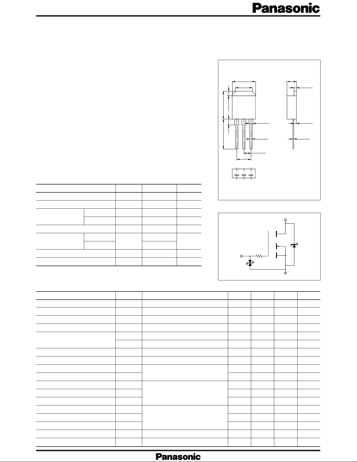
Power F-MOS FETs 2SK2339
G
S
D
2SK2339
Silicon N-Channel Power F-MOS
■ Features
●
Avalanche energy capability guaranteed
●
Low ON-resistance
●
No secondary breakdown
●
Low-voltage drive
■ Applications
●
Non-contact relay
●
Solenoid drive
●
Motor drive
●
Control equipment
●
Switching mode regulator
■ Absolute Maximum Ratings (Tc = 25˚C)
Parameter
Drain-Source breakdown voltage
Gate-Source voltage
Drain current
DC
Pulse
Avalanche energy capability
T
Allowable power
dissipation
C
Ta= 25˚C
Channel temperature
Storage temperature
* L= 5mH, IL= 5A, 1 pulse
= 25˚C
Symbol
V
DSS
V
GSS
I
D
I
DP
*
EAS
P
D
T
ch
T
stg
Rating
80±10
±15
±10
±20
62.5
30
1.3
150
–55 to +150
Unit
V
V
A
A
mJ
W
˚C
˚C
8.5±0.2
6.0±0.5
10.0±0.310.5min.
1.5max.
2.0 1.5±0.1
0.8±0.1
2.54±0.3
5.08±0.5
213
■ Equivalent Circuit
Unit : mm
3.4±0.3
1.0±0.1
1.1max.
0.5max.
1 : Gate
2 : Collector
3 : Emitter
N Type Package
■ Electrical Characteristics (Tc = 25˚C)
Parameter
Drain-Source cut-off current
Gate-Source leakage current
Drain-Source breakdown voltage
Gate threshold voltage
Drain-Source ON-resistance
Forward transadmittance
Diode forward voltage
Reverse recovery time
Reverse recovery charge
Input capacitance
Output capacitance
Feedback capacitance
Turn-on time
Fall time
Turn-off time (delay time)
Channel-Case heat resistance
Channel-Atmosphere heat resistance
Symbol
I
DSS
I
GSS
V
DSS
V
th
R
DS(on)
R
DS(on)
|
| Y
fs
V
DSF
t
rr
Q
rr
C
iss
C
oss
C
rss
t
on
t
f
t
d(off)
R
th(ch-c)
R
th(ch-a)
1
2
V
V
I
D
V
V
V
V
I
DR
L=230µ H, V
I
DR
V
V
V
Condition
= 70V, VGS= 0
DS
= 0, VGS=15V
DS
=1mA, VGS= 0
=10V, ID=1mA
DS
=10V, ID= 5A
GS
= 4V, ID= 5A
GS
=10V, ID= 5A
DS
=10A, VGS= 0
= 30V, VGS= 0
DD
=10A, di/dt= 80A/µ s
=10V , VGS= 0, f= 1MHz
DS
= 30V, ID= 5A
DD
=10V, RL= 6Ω
GS
Min
70
1
3
Typ
150
230
5.5
0.55
2.2
85
250
20
0.5
0.9
1.9
Max
10
±10
90
2.5
230
370
–1.8
4.2
96
Unit
µA
µA
V
V
mΩ
mΩ
S
V
µs
µs
pF
pF
pF
µs
µs
µs
˚C/W
˚C/W
Page 2
Power F-MOS FETs 2SK2339
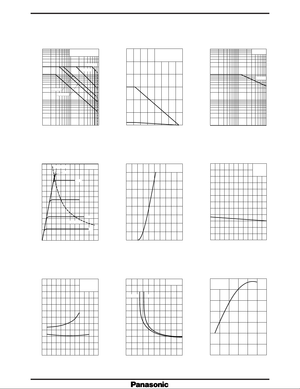
Area of safe operation (ASO)
100
30
I
DP
I
)
D
10
A
(
D
3
t=10ms
1
Drain current I
0.3
0.1
1
Drain-Source voltage V
14
12
10
)
A
(
D
8
6
Drain current I
4
2
0
V
024681012
Drain-Source voltage V
Non repetitive pulse
T
t=100ms
105503 30 100
I
D –VDS
=10V
GS
5V
PD=30W
=25˚C
C
DC
4.5V
DS
4V
DS
t=100ms
t=1ms
(V)
Ta=25˚C
3.5V
(V)
PD – Ta
60
)
50
W
(
D
40
30
20
Allowable power dissipation P
10
0
18
16
14
)
A
12
(
D
10
8
6
Drain current I
4
3V
2
0
40 80 120 16020 60 100 140
0
Ambient temperature Ta (˚C
246 108
0
Gate-Source voltage V
(1) TC=Ta
(2) Without heat sink
(P
(1)
(2)
ID – V
GS
=1.3W)
D
GS
)
TC=25˚C
(V)
100
50
30
20
)
A
(
10
AS
5
3
2
1
Abalanche current I
0.5
0.3
0.2
0.1
0.1
6
5
)
V
(
th
4
3
2
Gate threshold voltage V
1
0
IAS – L-load
TC=25˚C
62.5mJ
1100.5 50.3 3
– T
C
)
C
VDS=10V
I
=1mA
D
(˚C)
L-load L (mH
V
th
0 25 50 75 100 125 150
Case temperature T
R
600
)
Ω
500
(
DS(on)
400
300
200
100
Drain-Source ON-resistance R
0
024681012
Drain current I
DS(on)
(1)
(2)
– I
D
D
(1)VGS=4V
(2)V
GS
T
=25˚C
C
(A)
=10V
R
600
)
mΩ
(
500
(on)
DS
400
300
200
100
Drain-Source ON-resistance R
0
2468
010
Gate-Source voltage V
DS(on)
=5AID=2.5A
I
D
– V
GS
TC=25˚C
(V
GS
7
VDS=10V
Ta=25˚C
6
)
S
(
|
5
fs
4
3
2
Forward transadmittance | Y
1
0
010
)
| Yfs | – I
Drain current I
D
864212
(A)
D
Page 3

Power F-MOS FETs 2SK2339
C
iss, Coss, Crss
)
2000
F
(p
1000
rss
, C
oss
500
, C
iss
C
200
100
50
Feedback capacitance
20
10
5
Input capacitance, Output capacitance,
0 10020 40 60 80
Drain-Source voltage V
I
SD
20
10
5
(A)
3
SD
2
1
– V
– V
SD
f=1MHz
T
C
Coss
Ciss
Crss
DS
VGS=0
T
DS
=25˚C
(V)
=25˚C
C
t
d(off), tr, ton
3.0
2.5
)
2.0
ms
(
1.5
1.0
Switching time t
0.5
0
024681012
Drain current I
1000
Notes: R
and under natural convection.
(1) without heat sink
(2) with a 50 × 50 × 2mm Al heat sink
)
100
˚C/W
(
th
10
– I
D
VDD=30V
V
GS
T
=25˚C
C
t
d(off)
t
f
t
on
(A)
D
was measured at Ta=25˚C
th
=10V
)
V
(
DS
Drain-Source voltage V
Rth – t
P
V
DS, VGS
ID=10A
Ta=20˚C
60 12
V
DS
50 10
40 8
30 6
20 4
10 2
00
0 5 10 15 20 25
VDS=30V
VDS=40V
VDS=50V
Gate charge amount
– Q
V
GS
Qg
(1)
(2)
g
14
)
V
(
GS
V
Gate-Source voltage
(nc)
0.5
0.3
Souce-Drain current I
0.2
0.1
0.05
0.5 1.0 1.5
0 2.0
Diode forward voltage V
1
Thermal resistance R
0.1
–4
10
)
(V
SD
–3
10
–2
10
–1
10
Pulse width t
11010
(s)
P
2103
4
10
 Loading...