

Page 1

2SK2347
Ordering number : EN5424A
High-Voltage, High-Speed
Switching Applications
N-Channel Silicon MOSFET
SANYO Electric Co.,Ltd. Semiconductor Bussiness Headquarters
TOKYO OFFICE Tokyo Bldg., 1-10, 1 Chome, Ueno, Taito-ku, TOKYO, 110 JAPAN
72597TS (KOTO) TA-1033 No.5424-1/4
Package Dimensions
unit: mm
2131-TO-3JML
[2SK2347]
SANYO: TO-3JML
1 : Gate
2 : Drain
3 : Source
Specifications
Absolute Maximum Ratings
at Ta=25°C
Parameter Symbol Conditions Ratings Unit
Drain-to-Source Voltage V
DSS
1000 V
Gate-to-Source Voltage V
GSS
±30 V
Drain Current (DC) I
D
20 A
Drain Current (pulse) I
DP
PW≤10µs, duty cycle≤1% 40 A
Allowable Power Dissipation P
D
4.6 W
Tc=25°C 160 W
Channel Temperature Tch 150 °C
Storage temperature Tstg –55 to +150 °C
Electrical Characteristics at Ta=25°C
Parameter Symbol Conditions
Ratings
min typ max
Unit
D-S Breakdown Voltage V
(BR)DSSID
=1mA, VGS=0 1000 V
Zero-Gate Voltage Drain Current I
DSS
VDS=1000V, VGS=0 1.0 mA
Gate-to Source Leak Current I
GSS
VGS=±30V, VDS=0 ±100 nA
Cutoff Voltage V
GS(off)
VDS=10V, ID=1mA 1.5 3.5 V
Forward Transfer Admittance |yfs|V
DS
=20V, ID=10A 5.0 10 S
Static Drain-to-Source R
DS(on)
ID=10A, VGS=10V 0.6 0.8 Ω
ON-State Resistance
Input Capacitance Ciss VDS=20V, f=1MHz 3300 pF
Output Capacitance Coss VDS=20V, f=1MHz 750 pF
Reverse Transfer Capacitance Crss VDS=20V, f=1MHz 500 pF
Continued on next page.
Features
• Low ON resistance, ultrahigh-speed switching.
• High reliability (Adoption of HVP process).
Page 2

Continued from preceding page.
Parameter Symbol Conditions
Ratings
min typ max
Unit
Turn-ON Delay Time t
d(on)
45 ns
Rise Time t
r
ID=10A, VGS=10V, 200 ns
Turn-OFF Delay Time t
d(off)
VDD=200V, RGS=50Ω 900 ns
Fall Time t
f
250 ns
Diode Forward Voltage V
SD
IS=20A, VGS=0 1.5 V
Reverse Recovery Time t
rr
IS=20A, di/dt=100A/µs 0.5 1.0 µs
Switching Time Test Circuit
2SK2347
No.5524-2/4
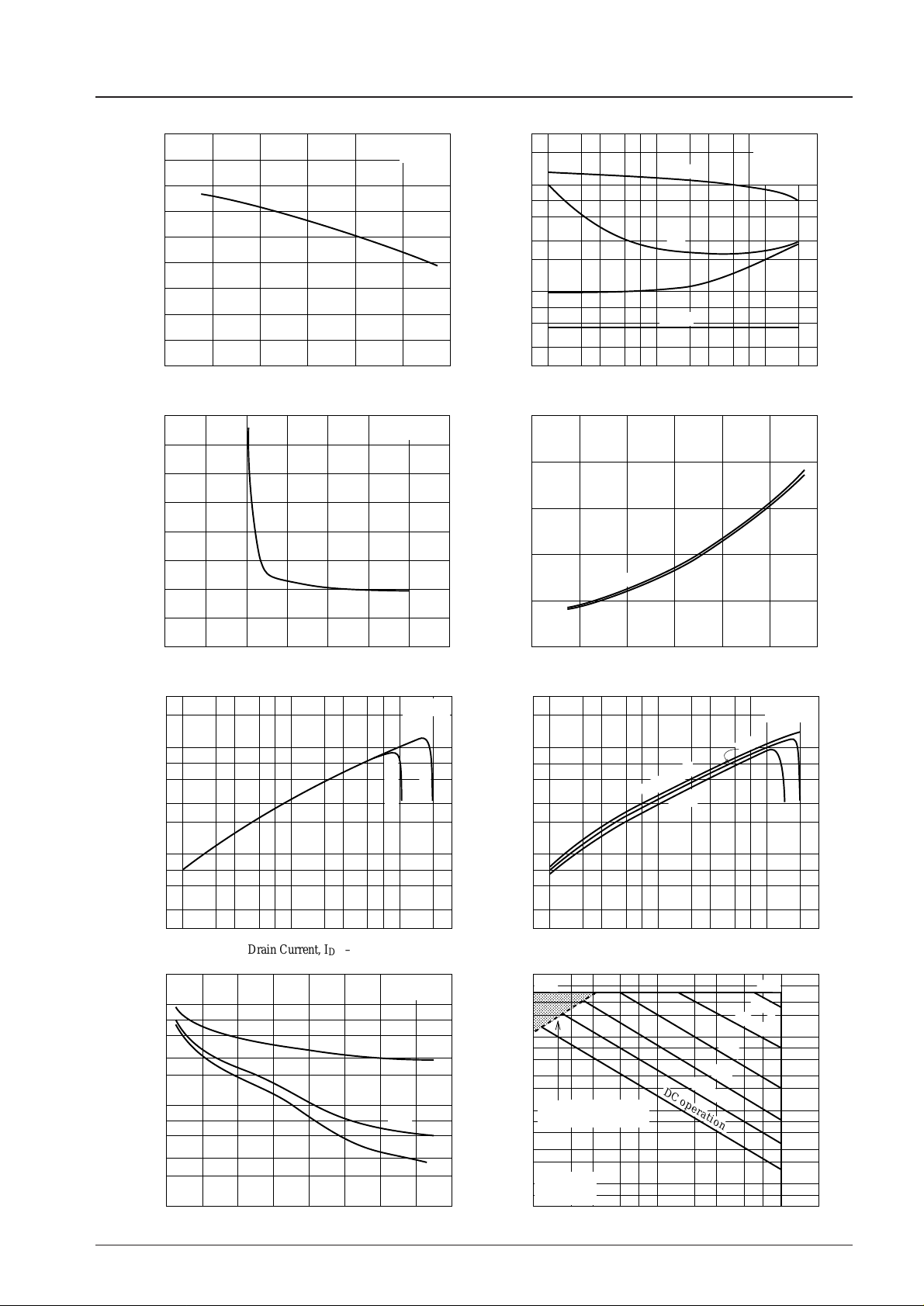
Drain Current, I
D
– ADrain Current, I
D
– A
Drain Current, I
D
– A Drain Current, I
D
– A
Drain-to-Source Voltage, VDS – V Drain-to-Source Voltage, VDS – V
Gate-to-Source Voltage, V
GS
– V
ID-
V
DS
ID-
V
GS
ID-
Tc
6 8 14
-
80
-
40 0 40 80 120 160
10 1242
0
0
4
8
12
24
20
16
32
28
40
36
0
4
8
12
16
20
24
28
32
36
40
ID-
V
DS
0 4 8 12 16 20
0
4
16
20
12
8
0
20
30
40
50
10
0 10 20 30 5040
V
GS
=10V
V
GS
=10V
6V
5V
3.5V
4V
4.5V
3V
3V
4V
5V
6V
V
G S
=10V
V
D S
=20V
10V
25°C
75°C
VDS=20V
Tc=
-
25°C
Case Temperature, Tc – °C
Page 3
2SK2347
No.5424-3/4
Drain Current, ID – A
Gate-to-Source Voltage, V
GS
– V
V
GS
(off)
-
Tc
-
80
-
40 0 40 80 120 160
-
80
-
40 0 40 80 120 160
1000
0.1
2
23355
7
2
3
2
3
5
7
7 2 3 2 35 7
1.0 10
100
0.8
1.2
1.6
0.4
0
2.0
7
60 42 12108 14
Cutoff Voltage, V
GS(off)
– V
Static Drain-to-Source
ON-State Resistance, R
DS(on)
– Ω
0
0.4
0.8
1.2
2.0
1.6
3.2
2.8
2.4
3.6
0.5
0.4
0.6
0.8
0.7
1.1
1.0
0.9
1.2
Case Temperature, Tc – °C
Case Temperature, Tc – °C
V
D S
=10V
20V
VDD=200V
V
GS
=10V
P.W.=1µs
D.C.≤0.5%
VDS=10V
I
D
=1mA
ID=10A
Tc=25°C
ID=10A
Switching Time, SW Time – ns
t
r
t
f
t
d(off)
t
d(on)
SW Time
-
I
D
R
DS
(on)
-
V
GS
R
DS
(on)
-
Tc
Static Drain-to-Source
ON-State Resistance, R
DS(on)
– Ω
DC operation
Drain Current, ID – A
Drain-to-Source Voltage, V
DS
– V Drain-to-Source Voltage, VDS – V
12 16 20 3224 28840
75
32
75
32 2
0.1
10 100 1000
1.0
10
2
3
5
7
5
7
2
3
5
7
2
3
5
7
1.0
10
2
3
5
7
2
3
2
3
5
7
1000
100
10000
2
3
5
7
2
3
2
5
7
1.0
10
2
3
5
7
2
3
2
3
5
7
V
DS
=10V
20V
25°C
75°C
Tc=25°C
Tc=25°C
Single pulse
Tc=–25°C
Ciss,Coss,Crss
-
V
DS
Ciss,Coss,Crss – pF
Ciss
Crss
Coss
Forward Transfer Admittance, |
y
fs | – S
Drain Current, ID – A
Forward Transfer Admittance, |
y
fs | – S
| y
fs
|
-
I
D
| y
fs
|
-
I
D
77 5
32
75
32 32
0.1 1.0 1.010
77 5
32
75
32 32
0.1 10
Drain Current, I
D
– A
ASO
100µs
10µs
5µs
I
DP
Operation in this area
is limited by R
DS
(on).
V
G S
=0
f=1MHz
V
D S
=20V
V
G S
=10V
1ms
10ms
100ms
Page 4
2SK2347
No.5424-4/4
No products described or contained herein are intended for use in surgical implants, life-support systems,
aerospace equipment, nuclear power control systems, vehicles, disaster/crime-prevention equipment and
the like, the failure of which may directly or indirectly cause injury, death or property lose.
Anyone purchasing any products described or contained herein for an above-mentioned use shall:
Accept full responsibility and indemnify and defend SANYO ELECTRIC CO., LTD., its affiliates,
subsidiaries and distributors and all their officers and employees, jointly and severally, against any
and all claims and litigation and all damages, cost and expenses associated with such use:
Not impose any responsibilty for any fault or negligence which may be cited in any such claim or
litigation on SANYO ELECTRIC CO., LTD., its affiliates, subsidiaries and distributors or any of
their officers and employees jointly or severally.
Information (including circuit diagrams and circuit parameters) herein is for example only; it is not guaranteed for volume production. SANYO believes information herein is accurate and reliable, but no guarantees
are made or implied regarding its use or any infringements of intellectual property rights or other rights of
third parties.
This catalog provides information as of July, 1997. Specifications and information herein are subject to
change without notice.
8060
100 120
160140
40
200
8060
100 120
160140
40
200
0
1
2
3
4.6
4
5
0
40
80
120
160
200
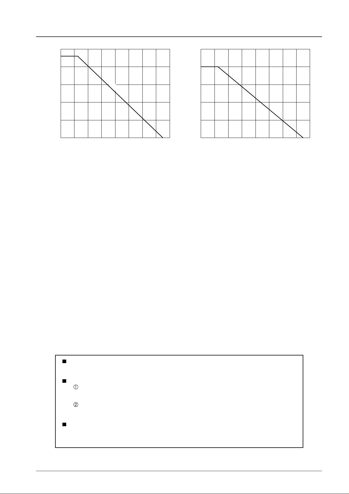
Allowable Power Dissipation, P
D
– W
Allowable Power Dissipation, P
D
– W
PD-
Ta
Ambient Temperature, Ta – °C
No heat sink
PD-
Tc
Case Temperature, Ta – °C
 Loading...