

Page 1
SERVICE MANUAL
(without price)
ELECTRONIC CASH REGISTER
CE-300 (EX-247)
JANUARY 1997
Printer Model : MD-910
Page 2

CONTENTS
Page
1. SPECIFICATIONS ................................................................................................ 1
2. INITIALIZE (MAC) OPERATION .......................................................................... 1
3. BLOCK DIAGRAM
3-1. PCB connection ......................................................................................... 2
3-2. Block diagram (circuit) .............................................................................. 3
4. CIRCUIT EXPLANATION
4-1. Power supply circuit.................................................................................. 4
4-2. CPU (uPD78052GC-093-3B9) .................................................................... 5
4-3. Display controller (uPD16312GB-3B4)..................................................... 7
4-4. Initialize IC (Reset circuit) ......................................................................... 8
4-5. Power down detection circuit (PWD) ....................................................... 8
4-6. Address latch circuit ................................................................................. 8
4-7. RAM / ROM bank selection circuit............................................................ 9
4-8. Head drive circuit for printer................................................................... 10
4-9. Vpp sensor circuit.................................................................................... 11
4-10. Power supply circuit for display............................................................. 11
5. DIAGNOSTIC
5-1. To start the diagnostic program............................................................. 12
5-2. Check item................................................................................................ 12
5-3. Operation of each test ............................................................................. 12
5-4. To exit the diagnostic test....................................................................... 17
6. ERROR CODE
6-1. Operation error code ............................................................................... 18
6-2. System lock code..................................................................................... 19
7. IC DATA
1. TC74HC00AP ............................................................................................ 20
2. TC74HC08AP ............................................................................................ 20
3. TC74HC138 ............................................................................................... 20
4. TC74HC367AP .......................................................................................... 21
5. TL431CLPB............................................................................................... 21
6. TC74HC373AP .......................................................................................... 21
7. S-80745 / S-80719..................................................................................... 22
8. M5237L...................................................................................................... 22
9. MAX232 ..................................................................................................... 22
8. PCB LAYOUT ..................................................................................................... 23
9. CIRCUIT DIAGRAMS ......................................................................................... 25
10. PARTS LIST ....................................................................................................... 41
Page 3

1. SPECIFICATIONS
Power consumption 120 V 220 V 230 V 240 V
In operation Max. 0.28 A 0.17 A 0.16 A 0.15 A
Stand by 0.14 A 0.09 A 0.08 A 0.07 A
Mode SW OFF Max. 0.12 A 0.08 A 0.07 A 0.06 A
Memory protection Backup battery Mangan Battery
UM-3 × 3 pcs.
Backup period 1 year (25 °C)
Battery life Replace the battery every 1 year.
Memory capacity 32 KB CXK58257AP-70/10L
Clock and calender Accuracy Within ±30 sec. per month (25 °C)
Auto calender Effective until 2099 A.D.
Environment Operating temperature 0 °C~40°C
Operating humidity 10 % ~ 90 %
Storage temperature -25 °C~65°C
Storage humidity 10 % ~ 95 %
Printer Model MD-910-SSC
Print method Dot matrix printing
Print digits 24 digits
MCBF 1,500,000 lines
Ink cassette Life 250,000 characters
Roll paper Type Fine-quality paper or Pressure-sensitive copy paper
Size 57.5 ±0.5 mm
Roll diameter 83 mm or less
2. INITIALIZE (MAC) OPERATION
1. Set the mode switch to “OFF” position.
2. Pressing the “FEED” button and turn the mode switch to “PRG” position.
3. Release the “FEED” button.
4. Press “#2” key (Normally “SUB TOTAL” key).
5. Initialize operation is executed.
— 1 —
Page 4
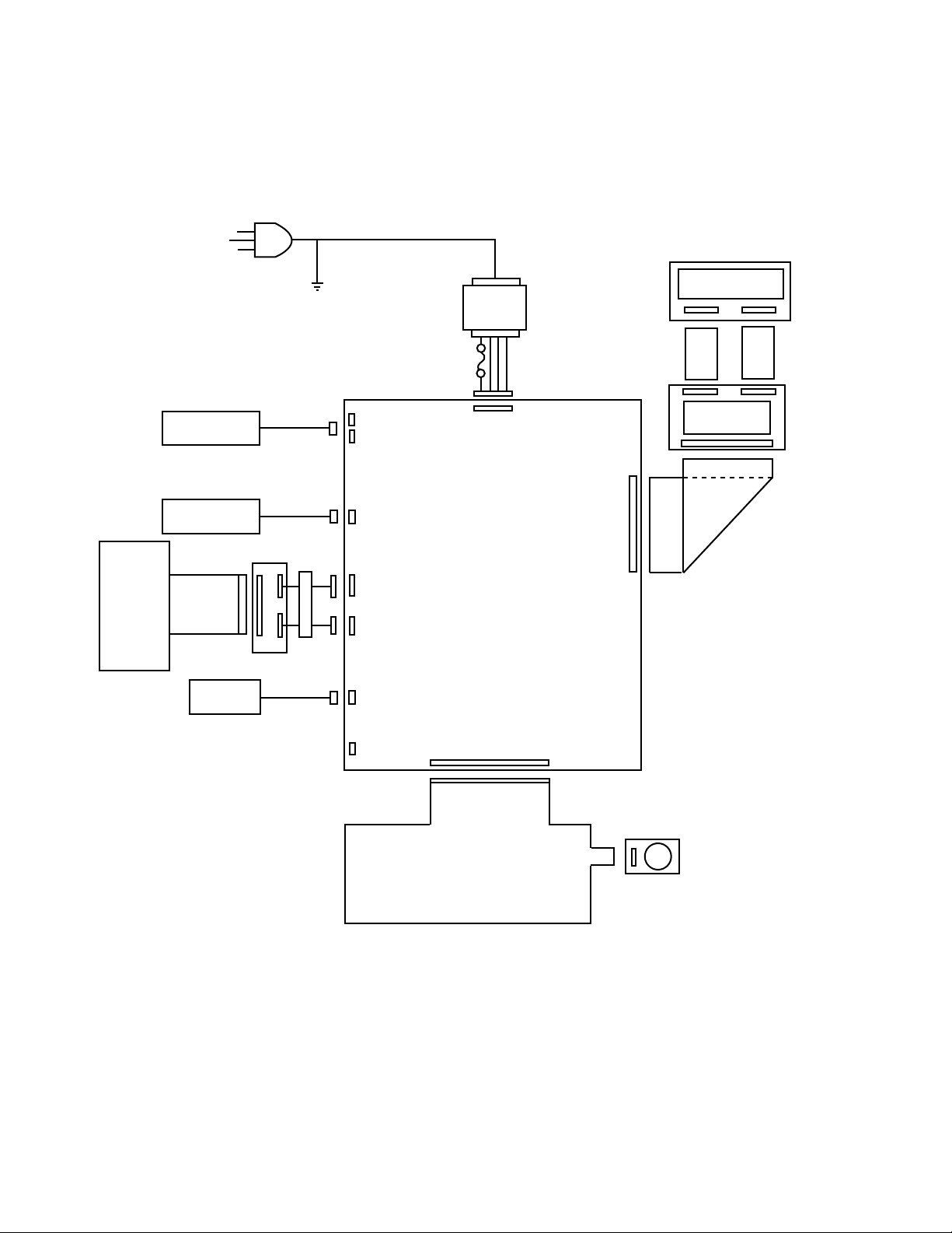
3. BLOCK DIAGRAM
3-1. PCB connection
Printer
(MD910SSC)
Mangan Battery
(UM-3 × 3)
Winder
Motor
E247-CNB
17P
Drawer
CORE
2 turn
3P
2P
10P
7P
3P
CN7
CN6
CN4
CN13
CN14
CN2
Fuse
E247-1
Transformer
4P
CN3
24P
Rear Display
(SH1019A)
12P10P
Main Display
(SH101MA)
E278-E2-2
E278-E2-1
9P
(RS232C)
CN17
FPC
CN16
25P
Mode SW
E266-E3-1
— 2 —
Page 5
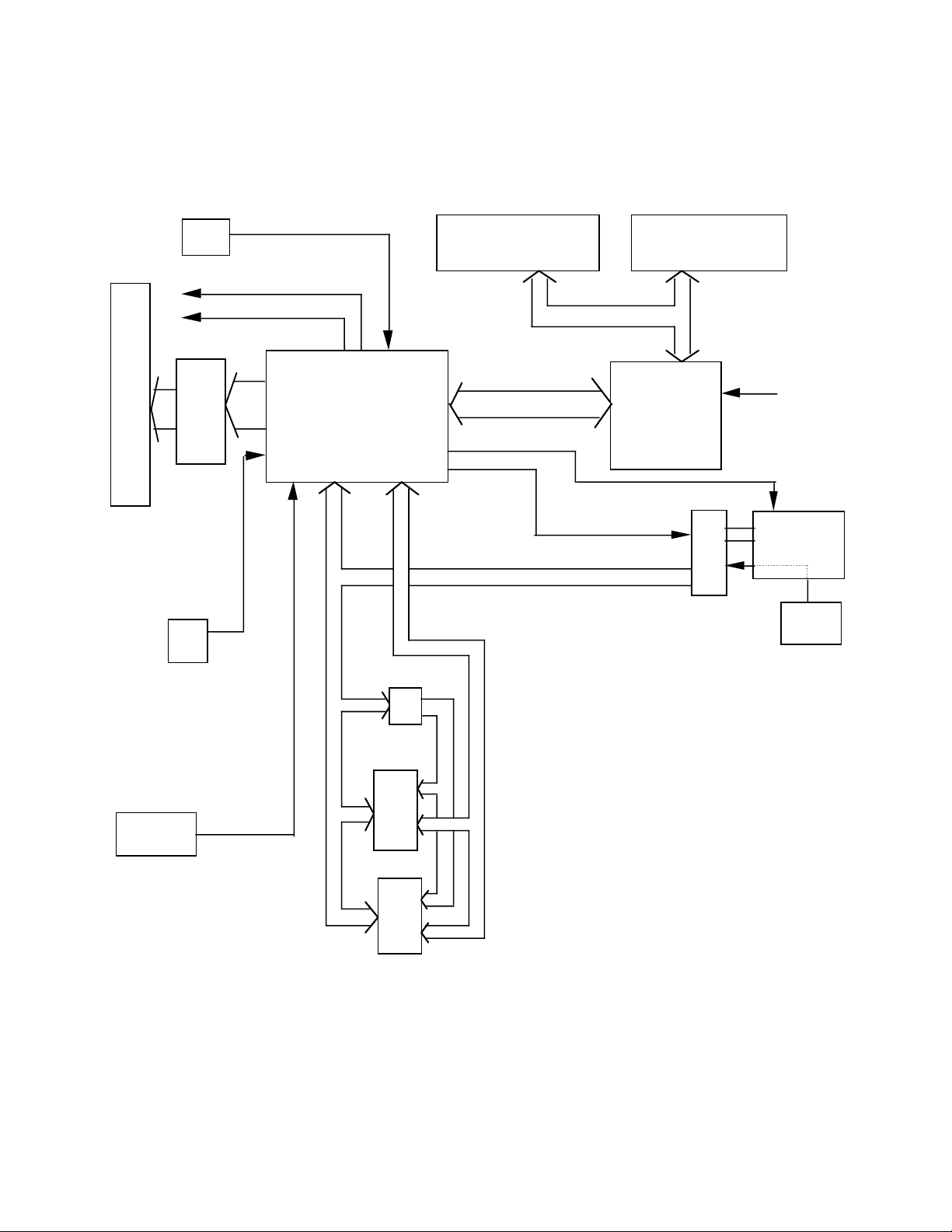
3-2. Block diagram (circuit)
Reset circuit
Printer
MD-910
S80719AN
MD
WD
Head drive cuicuit
HD.A~HD.H
CUSTOMER DISPLAY
SH1019A
MAIN DISPLAY
SH101MA
Segment & Digit data
PWD detection
CPU
uPD78052GC-093-3B9
AD0~AD7
ROM
A8~A15
A0~A7
DI,DO,CLK,STB
uPD16312GB3B4
Select addess
AD0~AD5
DRWS
KC0~KC4
Keyboard
FPC
Mode
Key
RS232C circuit
RAM
— 3 —
Page 6
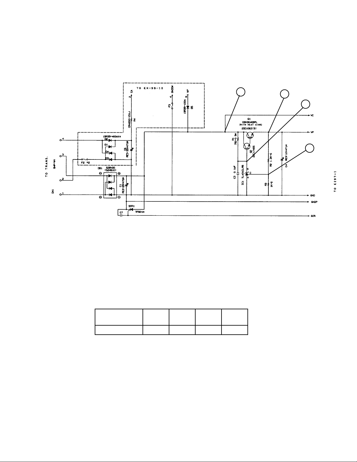
4. CIRCUIT EXPLANATION
4-1. Power supply circuit
Q1: Power transistor
Q2: Voltage detection transistor
A
B
C
D
Voltage level at above check point (unit: V )
Measurement
position
ABCD
Voltage (V) 12.5V 5.3V 6.2V 2.47V
— 4 —
Page 7
4-2. CPU (uPD78052GC-093-3B9)
Pin No. Signal Description In/Out
1 FB3 Not used — — —
2 FB4 RAM bank 3 Out High High
3 FB5 RAM bank 4 Out High High
4 AVSS GND — GND GND
5 PGM Not used — — —
6 RAM Chip select signal for RAM Out High Low
7 AVREF VDD — 5 V 5 V
8 RXD Receive data In High High
9 TXD Send data Ou t High High
10 WD Winder motor drive signal Out Low Low
11 DI Data signal from uPD16312 In Pulse High
12 DO Data signal to uPD16312 Out Pulse High
13 CLK Clock signal for uPD16312 Out Pulse High
14 STB Data strobe signal for uPD16312 Out Pulse High
15 KC0 Key common signal (KC0) Out Pulse High
16 KC1 Key common signal (KC1) Out Pulse High
17 KC2 Key common signal (KC2) Out Pulse High
18 KC3 Key common signal (KC3) Out Pulse High
19 AD0 Address / Data signal (AD0) In/Out Pulse High
20 AD1 Address / Data signal (AD1) In/Out Pulse High
21 AD2 Address / Data signal (AD2) In/Out Pulse High
22 AD3 Address / Data signal (AD3) In/Out Pulse High
23 AD4 Address / Data signal (AD4) In/Out Pulse High
24 AD5 Address / Data signal (AD5) In/Out Pulse High
25 AD6 Address / Data signal (AD6) In/Out Pulse High
26 AD7 Address / Data signal (AD7) In/Out Pulse High
27 A8 Address signal (A8) Out Pulse High
28 A9 Address signal (A9) Out Pulse High
29 A1 0 Address signal (A10) Out Pulse High
30 A1 1 Address signal (A11) Out Pulse High
31 A1 2 Address signal (A12) Out Pulse High
32 A1 3 Address signal (A13) Out Pulse High
33 VSS GND — GND GND
34 A1 4 Address signal (A14) Out Pulse High
35 A1 5 Address signal (A15) Out Pulse High
36 INIT PAD2 status — — —
3 7 VPP PAD1 status — — —
38 DSR Data set ready signal In High High
39 KC4 Key common signal (KC4) Out Pulse High
40 RD Output enable signal of RAM/ROM (RD) Out Pulse High
41 W R Write enable signal of RAM (WR) Out Pulse High
42 RA14 Address signal of ROM (Bank 0) Out High High
43 ASTB Latch enable for Address decoder (ASTB) Out Pulse Low
44 KI12 Key input signal (KI12) In High High
45 KI13 Key input signal (KI13) In High High
46 RA16 Address signal of ROM (Bank2) Out High High
47 RA15 Address signal of ROM (Bank 1) Out High High
48 MD Motor drive signal of printer (MD) Out Low Low
49 DRW Drawer drive signal (DRW) Out Low Low
50 BUZ Buzzer signal (BUZZ) Out Low Low
51 F D Paper feed signal of printer (FD) Out Low Low
52 HD.A Head drive signal of printer (HD.A) Out Low Low
53 HD.B Head drive signal of printer (HD.B) Out Low Low
54 HD.C Head drive signal of printer (HD.C) Out Low Low
55 HD.D Head drive signal of printer (HD.D) Out Low Low
— 5 —
Status of
Power On
Status of
Power OFF
Page 8
Pin No. Signal Description In/Out
Status of
Power On
56 HD.E Head drive signal of printer (HD.E) Out Low Low
57 HD.F Head drive signal of printer (HD.F) Out Low Low
58 HD.G Head drive signal of printer (HD.G) Out Low Low
59 HD.H Head drive signal of printer (HD.H) Out Low Low
6 0 RESET Reset signal (RESET) In High High
61 DP Dot pulse form printer (DP) In Low High
62 RP Reset pulse from printer (RP) In High High
63 OFF Mode key status (OFF) Out High Low
64 PWD Power down signal (PWD) In Low High
65 RB0 Address signal for RAM (Bank 0) Out High High
66 RB1 Address signal for RAM (Bank 1) Out High High
67 RB2 Address signal for RAM (Bank 2) Out High High
68 VDD VDD — 5 V 5 V
69 X2 System clock (5 MHz) In Pulse High
70 X1 System clock (5 MHz) In Pulse High
71 I C GND — GND GND
72 XT2 Sub system clock (32.768 KHz) In Pulse Pulse
73 XT1 Sub system clock (32.768 KHz) In Pulse Pulse
74 AVDD VDD — 5 V 5 V
75 AVREF0 VCC — GND GND
76 BAT Low battery signal In High High
77 VPP.S VPP detection signal (VPP.S) In Lo w Low
78 FB0 Address signal of Fiscal ROM bank 0 Out High High
79 FB1 Address signal of Fiscal ROM bank 1 Out High High
80 FB2 Address signal of Fiscal ROM bank 2 Out High High
Status of
Power OFF
— 6 —
Page 9
4-3. Display controller (uPD16312GB-3B4)
Pin No. Signal Description In/Out
1 SW1 Not used (GND) — GND GND
2 SW2 Not used (GND) — GND GND
3 SW3 Not used (GND) — GND GND
4 SW4 Not used (GND) — GND GND
5 DOUT Data out signal to CPU Out High High
6 DI N Data in signal from CPU In Pulse High
7 VSS GND — GND GND
8 CLK Clock signal (CLK) In Pulse High
9 STB Data strobe signal (STB) In Pulse High
1 0 KEY1 Not used — — —
1 1 KEY2 Not used — — —
12 KEY3 Draw er sensor signal (DRW.S) I n High High
13 KEY4 VCC — 5 V 5 V
14 VDD VCC — 5 V 5 V
1 5 SEG1 Display segment signal (Sa) Out Pulse Low
1 6 SEG2 Display segment signal (Sb) Out Pulse Low
1 7 SEG3 Display segment signal (Sc) Out Pulse Low
1 8 SEG4 Display segment signal (Sd) Out Pulse Low
1 9 SEG5 Display segment signal (Se) Out Pulse Low
2 0 SEG6 Display segment signal (Sf) Out Pulse Low
2 1 SEG7 Display segment signal (Sg) Out Pulse Low
2 2 SEG8 Display segment signal (Sdp) Out Pulse Low
2 3 SEG9 Display segment signal (Str) Out Pulse L ow
2 4 SEG10 Display segment common signal (Scom) Out Pulse Low
2 5 SEG11 Not used Low Low
2 6 SEG12 Not used Low Low
27 VEE Power for display (-VN) — -32 V -32 V
28 GRD10 Display digit signal (G10) Out Pulse L ow
29 GRD9 Display digit signal (G9) Out Pulse Low
30 GRD8 Display digit signal (G8) Out Pulse Low
31 GRD7 Display digit signal (G7) Out Pulse Low
32 GRD6 Display digit signal (G6) Out Pulse Low
33 GRD5 Display digit signal (G5) Out Pulse Low
34 GRD4 Display digit signal (G4) Out Pulse Low
35 GRD3 Display digit signal (G3) Out Pulse Low
36 GRD2 Display digit signal (G2) Out Pulse Low
37 GRD1 Display digit signal (G1) Out Pulse Low
38 VDD VCC — 5 V 5 V
39 LED4 Not used — Pulse Low
40 LED3 Not used — Pulse Low
41 LED2 Not used — Pulse Low
42 LED1 Not used — Pulse Low
43 VSS GND — GND GND
44 OSC System clock (500 KHz) In Pulse Pulse
Status of
Power On
Status of
Power OFF
— 7 —
Page 10
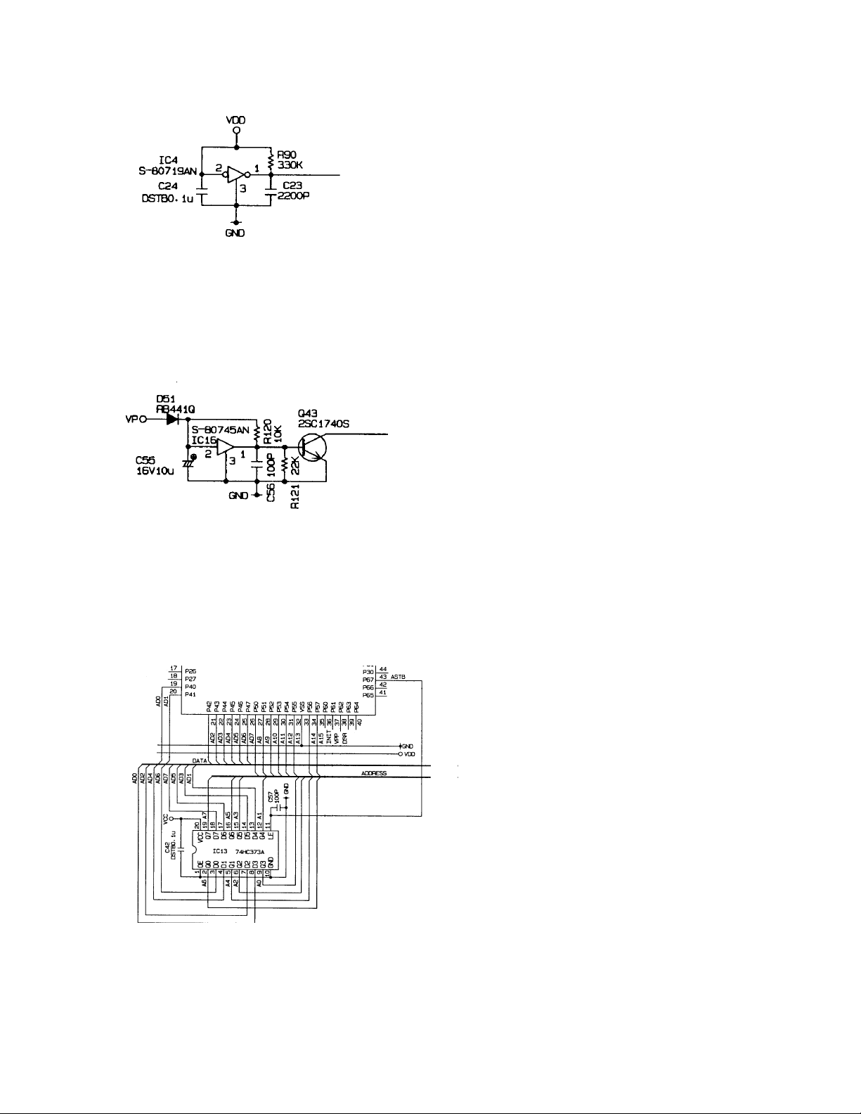
4-4. Initilize IC (Reset circuit)
VDD: Voltage of memory protection battery
To Pin No.60 of CPU
When the voltage level at Pin No.60 of CPU is not stabilized, CPU does not work properly in rare case.
Therefore, this machine uses the initialize IC for stabilizing the voltage.
Even the voltage level of VDD (Pin No.2) is changed, Pin No.1 of initilize IC outputs stabilized 5 volts.
When the VDD voltage become less than 1.9 V, the initialize IC send a reset signal to CPU.
4-5. Power down detection circuit (PWD)
To Pin No.64 of CPU
When the VP voltage become less than 4.8 V, the pin No.1 of IC5 become “Low” level.
Then,the transistor Q44 become OFF.
When Q44 become OFF, the voltage lebel of pin No.64 of CPU changes to “High” level from “Low”. Then,
CPU knows power failure.
4-6. Address latch circuit
CPU uses 8 port (AD0 ~ AD7) for address bus and
data bus.
To select the address, CPU use the IC13.
CPU send the address to IC13, and send ASTB
signal at same time.
Then, IC13 store the address and output the
address immediately.
In this way, CPU select the address and data
signal.
— 8 —
Page 11
4-7. RAM / ROM bank selection circuit
This circuit is used for address decoder for memory.
0000
2000
Memory Map
Mask ROM
(16 K)
00001
000000
Bank
0
4000
EP ROM
6000
Common (16 K)
8000
EP ROM
Bank select area
A000
(16 K)
C000
RAM common area
(8 K)
E000
RAM BANK select
area (4 K)
F000
Outer I/O area
FA80
Internal RAM
(High speed access)
FFFF
— 9 —
RAM 256 K
00011
00010
Bank
Bank
1
KI signal port (F800,F801)
2
Bank
3
Buffer RAM 32 bytes
Internal RAM
(High speed access)
288 bytes
Internal RAM
(High speed access)
Short direct area
192 bytes
General purpose
register 32 bytes
Special function
register (SFR)
256 bytes
00100
Bank
4
00101
00110
Bank
5
F800
FAC0
FAE0
FD00
FE20
FEE0
FFF0
RAM 1 M
11101
Bank
29
Page 12
4-8. Head drive circuit for printer
TR5
TR4
TR3
TR1
TR2
Motor drive circuit
Normally, the transistor of motor drive circuit is followng condition.
TR1, TR2, TR5 : OFF
TR3, TR4 : ON
MD (-) signal : VP level
When the CPU want to rotate the motor, CPU change the MD signal to “High” from “Low”.
Then, TR1, TR2 and TR5 are become ON and MD (-) signal is become GND level,
and then motor is rotated.
Head drive circuit
When the CPU wants to print, CPU send “High” signal from HD.A ~ HD.H terminal.
This signal goes to printer unit, and then print.
RP: Reset pulse from printer
DP: Dot pulse from printer
— 10 —
Page 13
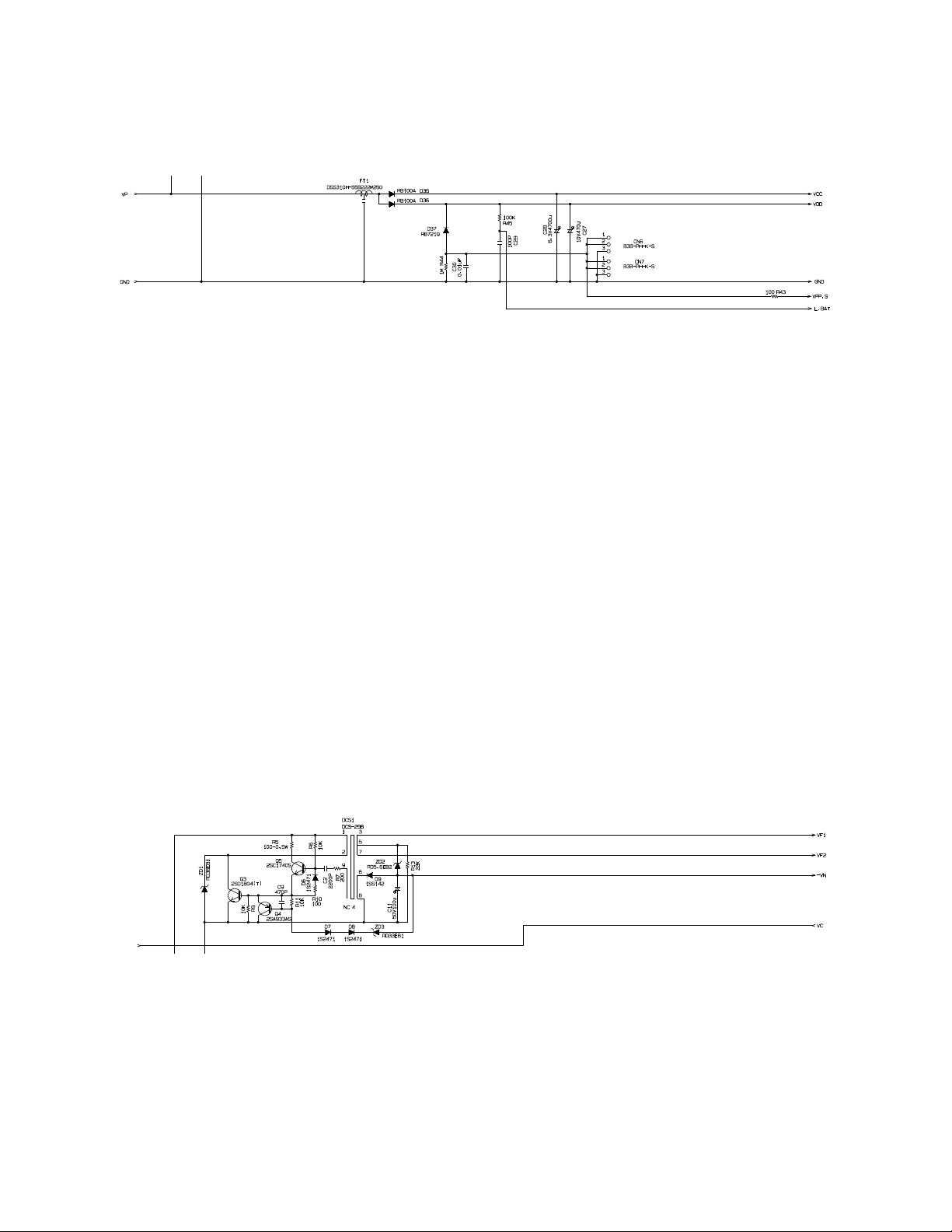
4-9. VPP sensor circuit
Protection circuit
To prevent the circuit breakage, the protection circuit watches the voltage level of VCC, VDD and VPP.
When the each voltage level is more than following condition, this circuit cuts the voltage.
VCC,VDD: In case these voltages are become over voltage, this circuit outputs “SCR”
signal(High signal) and burn out the fuse.
VPP: In case the VPP voltage is more than 15 V or less than 13.9 V, the “VPP.S” level
is inverted and CPU cut the “VPP.ON” signal.
Detection voltage level (Unit: V)
VCC >= +6.5 V
VDD >= +6.5 V
+13.9 V =< VPP <=15.0 V
4-10. Power supply circuit for display
VC
GNDVP
This circuit is making the power for display tube.
Voltage level: -VN Est. -31.2 V
VF1 - VF2 Est. AC4.85 V
— 11 —
Page 14
5. DIAGNOSTIC
5-1. To start the diagnostic program
1. Set the mode switch to “OFF” position.
2. Pressing the “FEED” button and turn the mode switch to “PRG” position.
3. Release the “FEED” button.
4. Input “9999900000” and press “ST” (“#2” key).
5. Diagnostic program is executed.
5-2. Check item
The following test can be checked in the diagnostic test.
1. Key code test
2. Switch status test
3. Individul function test.
5-3. Operation of each test
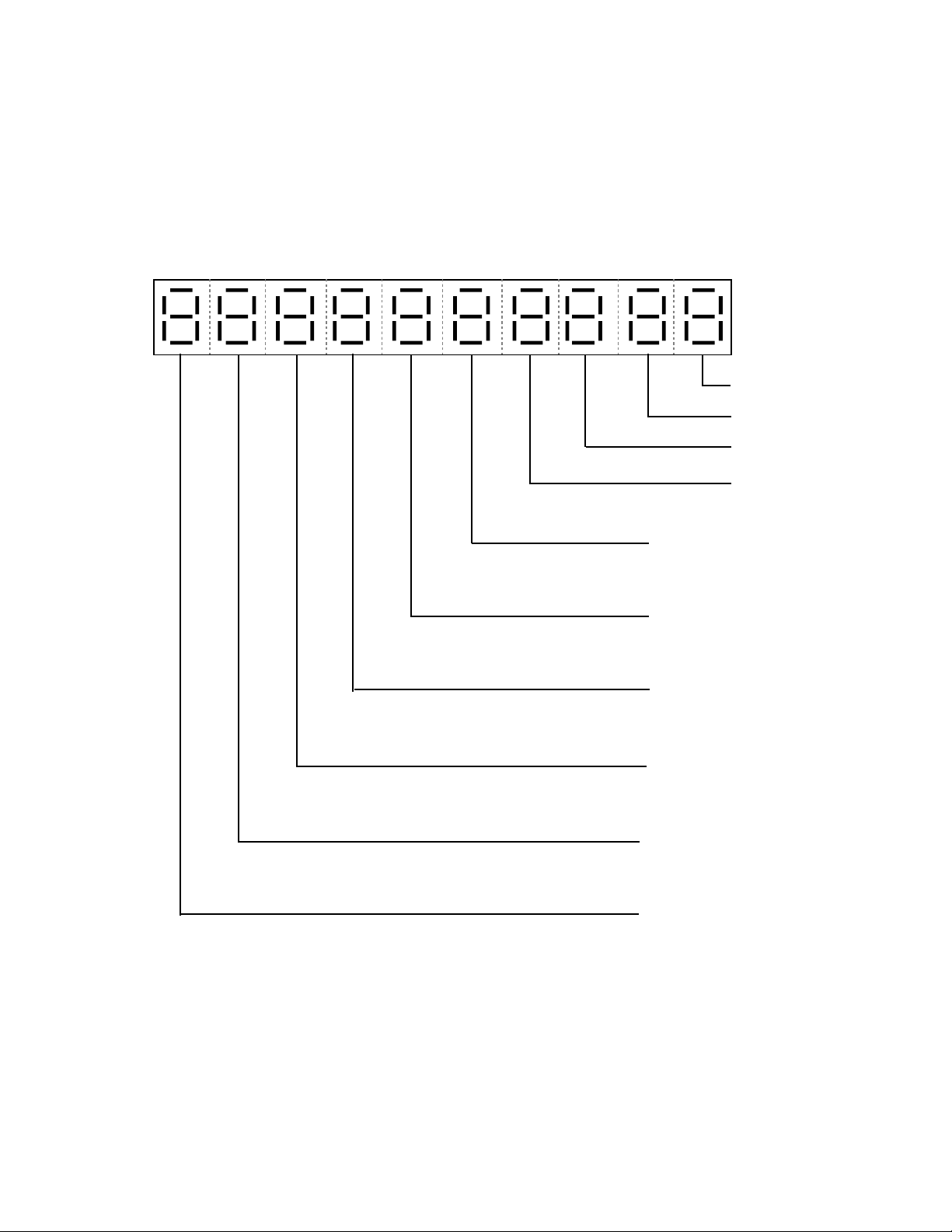
1. Key code test
When pressing a key, the machine displays
the following key code.
HARD KEY CODE TABLE
FEED 055 051 789046 040 034 028 022 016
058 054 050 456045 039 033 027 021 015
057 053 049 123044 038 032 026 020 014
056 052 C0011 012 043 037 031 025 019 013
DISPLAY
0 1 3
Hard key code
048 042 036 030 024 018
047 041 035 029 023 017
“020” & “026” buttons are work for “#2” key.
— 12 —
Page 15
2. Switch status test
Press “C” button, the switch status is appeared on the display.
[DISPLAY]
No display
No display
No display
No display
Low battery
L: Low battery
Nil: Battery OK
PAD2 status
1: Short
0: Open
PAD1 status
1: Short
0: Open
Always: 1
Drawer sensor
1: Close
0: Open
Mode switch status
1: PGM
2: RF
3: REG
4: CAL
5: X
6: Z
No display: OFF
— 13 —
Page 16
3. Individual function test
3-1. Series test
“Y” “X” “1” + “#2” key
Y: 0: Normal test
1: Execute next test even if an error happend at ROM check sum
X: 0: Autockecking of RAM capacity
1: 256 Kbit RAM test
2: 1 Mbit RAM test
Execute the following test in order.
1. Display test
2. Check sum test of EP-ROM
3. RAM test
4. Drawer open test
5. Printing test
6. Date and Time test
1. Display test (All segment light on)
2. Ckeck sum test of EP-ROM
Normal end Error end
ROM SUM OK
XX00: Check sum value XXXX : Check sum value
3. RAM test (Read/Write test)
Normal end receipt
256 Kbit RAM 1 Mbit RAM
Error end receipt
RAM 32K E R
4. Drawer open test
5. Printing test
BBBBBBBBBBBBBBBBBBBBBBBB
YY: Bank
XXXX: Address
ROM E R
RAM 128K R/W OK RAM 32K R/W OK
6. Date and Time test
Set the date and time as follows.
Date : 31 / 12 / 96 Time : 25:59
Then, issues a receipt and display the following character.
1 2. 3 4 5. 6 7 8. 9 0
— 14 —
Page 17

3-2. Print test
Input “Y” “X” “2” + “#2” key.
X: 0: Print the following character continuously.
Printing speed : 45 times / Min.
1: Print the following character, open the drawer and issue a receipt
Printing speed : 25 times / Min.
Drawer open : 5 times / Min.
Receipt issue : 5 times / Min.
Y: 0: No effect
1: Print the following character without waiting time. ( Continuously print )
To stop this test, press any key or turn the mode switch to “OFF” position.
Printing sample:
3-3. RAM read only test
Input “X” “5” + “#2” key.
X: 0: Read the data from start to end address and issues receipt.
1: Read the data from start to end address continuously until power off.
Brink " - " signal on the display during checking.
Note: Be sure to execute the series test ( 1 + #2 ) before this test.
256 Kbit check receipt 1 Mbit check receipt
Display
3-4. INIT OPERATION (To set a Factory Default setting)
Input “8” “6” + “#2” key.
BBBBBBBBBBBB
RAM 128K READ OK RAM 32K READ OK
The machine is executed a INIT operation according to PAD status.
Set the data and time to “0”.
(00-00-00, 00:00:00)
3-5. Voltage check for Memory protection battery
Input “7” + “#2” key.
Display the battery voltage.
To stop this test, press any key or turn the mode switch to “OFF” position.
X XX
X.XX: Voltage value
— 15 —
Page 18

3-6. All character print test
Input “8” + “#2” key.
“8” + “#2”: Pirnts all character on receipt once.
“1” “8” + “#2”: Prints all character on receipt continuously.
To stop this test, press any key or turn the mode switch to “OFF” position.
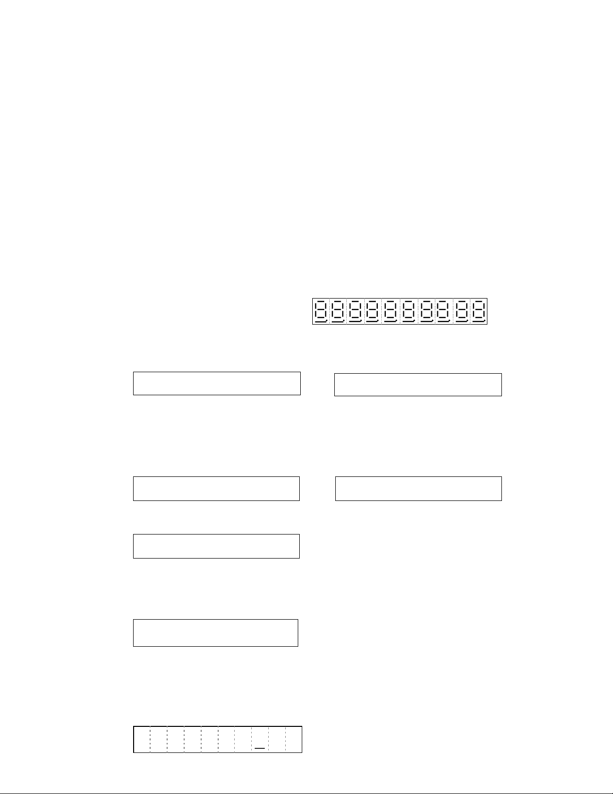
3-7. Time display test
Input “9” + “#2” key.
Display the time.
To stop this test, press any key or turn the mode switch to “OFF” position.
2 3 - 5 9 0 0
— 16 —
Page 19

3-8. RS232C port test
Input “2” “0” “7” + “#2” key.
Execute the RS232C loop back test continuously using loop back connector.
In case an error happens, the machine issues an error receipt then stop this test.
Test description: 1: Level check at DSR signal ( Low/High)
2: Send the data (05Ah) from TxD and receive it at RxD terminal.
To stop this test, turn the mode switch to “OFF” position.
Loop back connection:
TxD 2
RxD 3
DSR 6
Normal End Error End
232C OK
232C ER
X: Error code
0: Time over
1: Over run error
2: Framing error
3: RXD line data error
4: DSR line receive error
5-4. To exit the diagnostic test
To escape the diagnostic test mode, execute “INITIALIZE (MAC) operation”.
X
— 17 —
Page 20

6. ERROR CODE
6-1. Operation error code
Error codes appear on display whenever you make a mistake during operation.
Error Code
E01
E08
E27
E31
E33
E35
E38
E94
Meaning
Mode switch position changed before finalization.
Registration without entering a clerk number. This
error appears only when the clerk control function
is activated.
Transaction cancel buffer full.
Finalization of a transaction attempted without
confirming the subtotal.
Finalize operation attempted without entering
amount tender.
Change amount over.
Read/reset operation without declaring cash in
drawer. This error appears only when this function
is activated.
Printer error.
Action
Return the mode switch to its original
setting and finalize the operation.
Enter a clerk number.
Finalize the transaction.
Press the
SUB
TOTAL
key.
Enter the amount tendered.
Require small money.
Perform money declaration.
Turn the power off, and remove jammed
paper from the printer.
Press
C
key and check the appropriate section of this manual for the operation you want to perform.
C/AC
— 18 —
Page 21

6-2. System lock code
The following error code appears on display and receipt when the machine is lock up.
Execute the Flag MAC or MAC operation to clear these errors.
Error code: Display: X - - - - - - - - -
Receipt: X ! ! ! ! ! ! ! ! ! ! ! ! ! ! ! ! ! !
X: Lock code
Error sample: 3 ! ! ! ! ! ! ! ! ! ! ! ! ! ! ! ! ! !
Error code Error Name Meaning
1 Sequential trap The machine try to write to accumulator when the CPU is
hung up.
2 Memory write error Error happens when the CPU write the data to memory.
3 Trap error Abnormal address
6 Timer error Interrupt timer error
7 Stack over Abnormal address or stack pointer has an error
0 Other error CPU executes wrong jump vector before detect 1, 3 and
6 error code.
— 19 —
Page 22

7. IC DATA
1. TC74HC00AP
3. TC74HC138
2. TC74HC08AP
— 20 —
Page 23

4. TC74HC367AP 5. TL431CLPB
6. TC74HC373AP
— 21 —
Page 24

7. S-80745 / S-80719
8. M5237L
IN
Start up
Heat
protection
STD.
Voltage
ASO
protec
OP AMP
Current
protection
Out
tion
Voltage
adjust
9. MAX232
Terminal
IN
GND
Voltage adjust
GND
— 22 —
Page 25

8. PCB LAYOUT
MAIN PCB (E247-1) and Connector PCB (E247-CNB)
— 23 —
Page 26

9. CIRCUIT DIAGRAMS
BCDEFGHI JKA
1
2
3
4
1
2
3
4
5
6
7
8
5
6
7
8
Description: Board No. Drawing No.
LOCATION OF PRINTED
CIRCUIT BOARDS
E240450
BCDEFGHI JKA
— 25 —
Page 27

BCDEFGHI JKA
1
2
3
4
1
2
3
4
5
6
7
8
PAD condition
PAD1
PAD2
B.D.Bu
Open
Short
G
Short
Short
Description: Board No. Drawing No.
E240451E247-1 (1/8)MAIN PCB
5
6
7
8
BCDEFGHI JKA
— 26 —
Page 28

BCDEFGHI JKA
1
2
3
4
1
2
3
4
5
6
7
8
5
6
7
8
Description: Board No. Drawing No.
E240452E247-1 (2/8)MAIN PCB
BCDEFGHI JKA
— 27 —
Page 29

BCDEFGHI JKA
1
2
3
4
1
2
3
4
5
6
7
8
5
6
7
8
Description: Board No. Drawing No.
E240453E247-1 (3/8)MAIN PCB
BCDEFGHI JKA
— 28 —
Page 30

BCDEFGHI JKA
1
2
3
4
1
2
3
4
5
6
7
8
5
6
7
8
Description: Board No. Drawing No.
E240454E247-1 (4/8)MAIN PCB
BCDEFGHI JKA
— 29 —
Page 31

BCDEFGHI JKA
1
2
3
4
1
2
3
4
5
6
7
8
5
6
7
8
Description: Board No. Drawing No.
E240455E247-1 (5/8)MAIN PCB
BCDEFGHI JKA
— 30 —
Page 32

BCDEFGHI JKA
1
2
3
4
1
2
3
4
5
6
7
8
5
6
7
8
Description: Board No. Drawing No.
E240456E247-1 (6/8)MAIN PCB
BCDEFGHI JKA
— 31 —
Page 33

BCDEFGHI JKA
1
2
3
4
1
2
3
4
5
6
7
8
5
6
7
8
Description: Board No. Drawing No.
E240457E247-1 (7/8)MAIN PCB
BCDEFGHI JKA
— 32 —
Page 34

BCDEFGHI JKA
1
2
3
4
1
2
3
4
5
6
7
8
5
6
7
8
Description: Board No. Drawing No.
E240458E247-1 (8/8)MAIN PCB
BCDEFGHI JKA
— 33 —
Page 35

ABCD
1
2
3
4
5
6
1
2
3
4
5
6
ABCD
Description: Board No. Drawing No.
E440522E247-CNBE247-CNB
— 34 —
Page 36

BCDEFGHI JKA
1
2
3
4
1
2
3
4
5
6
7
8
5
6
7
8
Description: Board No. Drawing No.
E240465KEYBOARD
BCDEFGHI JKA
— 35 —
Page 37

ABCD
1
2
3
4
5
6
1
2
3
4
5
6
ABCD
Description: Board No. Drawing No.
E440523E278-E2-1MAIN DISPLAY
— 36 —
Page 38

ABCD
1
2
3
1
2
3
4
5
6
Description: Board No. Drawing No.
ABCD
4
5
6
E440524E278-E2-2CUSTOMER DISPLAY
— 37 —
Page 39

ABCDEFGH
1
2
3
1
2
3
4
5
4
5
Description: Board No. Drawing No.
6
E340638POWER SUPPLY CIRCUIT
6
ABCDEFGH
— 38 —
Page 40

ABCD
1
2
3
1
2
3
4
5
6
Description: Board No. Drawing No.
ABCD
— 39 —
4
5
6
E440525BATTERY
Page 41

10. PARTS LIST
1. Main PCB block E247-1 ass’y.................................................................... 43
2. Main display block E247-E2-1.................................................................... 47
3. Customer display block E247-E2-2............................................................ 47
4. Button ass’y................................................................................................ 48
5. Upper case ass’y........................................................................................48
6. Lower case ass’y........................................................................................48
7. Total component ........................................................................................ 49
8. Cash drawer (DL-2763).............................................................................. 50
9. Printer......................................................................................................... 52
Notes:
1. Prices and specifications are subject to change without notice.
2. As for order / supply of spare parts, refer to the "GUIDEBOOK for Spare Parts Supply", a separate
publication.
3. The numbers in item column correspond to the same numbers in drawing.
4. MARKS:
Q: Quantity used per unit
R: Rank
A: Essential
B: Stock recommended
C: Less recommended
X: No stock recommended
— 41 —
Page 42

55
56
63
62
66
51
43
49
46
47
59
58
57
52
60
61
42
44
48
E247-CNB
Drawer
E247-1 ass’y
53
45
54
64
5
65
2
40
41
7
8
6
3
4
39
50
1
Keyboard
Exploded Diagram
— 43 —
Page 43

12
14
15
17
20
24
19
18
16
13
11
22
23
21
38
25
26
27
33
32
31
30
9
10
29
28
35
34
37
36
Keyboard Block
— 44 —
Page 44

CE-300
Item Code No. Parts Name Specification Version Q R
1. Main PCB block E247-1 ass’y
6193 4726 Main PCB ass'y E247-1 E240425*2 All countries 1 A
IC2 2006 1207 LSI UPC16312GB-3B4 1 A
IC11 2006 1655 LSI UPD78052GC-093-3B9 1 A
IC14 2006 1354 LSI TMS27C512-12/15JL 1 A
IC15 2006 1319 RAM CXK58275AP-70/10L 1 A
IC26 2101 0189 MOS IC TC74HC138AP 1 A
IC18, 2105 1008 C-MOS IC TC74HC00AP 3 A
IC20-21
IC13 2105 1169 C-MOS IC TC74HC373AP 1 A
IC17,19 2105 1218 C-MOS IC TC74HC08AP 2 A
IC23-25 2112 0035 MOS IC TC74HC367AP 3 A
IC27 2112 0329 Bipolar IC MAX232N 1 A
IC4 2112 0336 Reset IC S-80719AN-Z 1 A
IC16 2112 0406 Reset IC S-80745AN-Z 1 A
IC1 2120 7349 Regulator IC TL431CLPB 1 A
Q38 2210 7186 Transistor 2SB926(T,U)-AA 1 B
Q14 2230 3902 Transistor 2SD1111-AA 1 B
Q15 2230 4135 Transistor 2SD1853-AA 1 B
Q20-21,23 2230 5261 Transistor 2SD965(P.Q.R)-TA 10 B
Q25,27,29
Q31,33,35
Q37
Q18,22,24 2250 0847 Digital transistor DTC143ZS-TP 12 B
Q26,28,30
Q32,34,36
Q40-42
Q3 2250 1309 Transistor 2SD1804(T) 1 B
Q4 2250 1323 Transistor 2SA933AS(QRS)TP 1 B
Q2,5,19, 2250 1330 Transistor 2SC1740S(QRSE)TP 5 B
Q39,43
Q1 2250 1554 Transistor 2SD1063(R,S) 1 B
ZD1 2315 2661 Zener diode RD36EB1-T1 1 B
ZD9-16 2315 2836 Zener diode RD20EB2-T1 8 B
ZD2 2315 3109 Zener diode RD5.6EB2-T1 1 B
ZD3 2315 3112 Zener diode RD33EB1-T1 1 B
DB1 2315 2857 Diode stack S2VB20 1 B
D6-8,10-29 2301 0046 Diode 1S2471 T-77-T 23 B
D9 2315 2619 Diode 1SS142-T-77-T 1 B
D38,40, 2315 2682 Diode 1SR35-100A-T-82 4 B
D49,50
D37 2315 2864 Diode RB721Q-T-77 1 B
D35,36 2390 0882 Schottky barrier diode RB100AT-32 2 B
D51 2390 1967 Diode RB441QT-77 1 B
X2 2408 8261 Ceramic oscillator CST5.00MGW 1 B
X1 2520 3445 Crystal oscillator C-002RX(M90-76) 1 B
DCS1 3000 7623 DC/DC converter DCS-298 1 A
R51 Carbon film resistor CR-25-2.2KOHMJ-T 1 X
R7 Carbon film resistor CR-25-200OHMJ-T 1 X
— 45 —
Page 45

Item Code No. Parts Name Specification Version Q R
R10,19,43 Carbon film resistor CR-25-100OHMJ-T 20 X
R52-54,
R84,85,94,
R99,100,
R103-105,
R108,109,
R128-131
R86,111, Carbon film resistor CR-25-1KOHMJ-T 5 X
R112,116,
R118
R33,47,87 Carbon film resistor CR-25-4.7KOHMJ-T 3 X
R6,9,11, Carbon film resistor CR-25-10KOHMJ-T 18 X
R20,23,46
R88,89,93,
R95,96,98,
R106,107,
R110,114,
R120
R90 Carbon film resistor CR-25-330KOHMJ-T 1 X
R44 Carbon film resistor CR-25-1MOHMJ-T 1 X
R97,119 Carbon film resistor CR-25-220OHM-J-T 2 X
R28 Carbon film resistor CR-25-3.3KOHM-J-T 1 X
R13-14, Carbon film resistor CR-25-22KOHM-J-T 4 X
R117,121,
R92 Carbon film resistor CR-25-680K-OHM-J-T 1 X
R5 Carbon film resistor R-50XT-24J101 1 X
R1 Carbon film resistor R-50X-750-J 1 X
R2 Carbon film resistor R-25-1.2K-G-T24-T 1 X
R3 Carbon film resistor R-25-1K-G-T24-T 1 X
R16,122, Carbon film resistor R-25-56K-J-T24-T 5 X
R124,126,
R127
R17 Carbon film resistor R-25-51K-J-T24-T 1 X
R45 Carbon film resistor R-25-100K-J-T24-T 1 X
R18 Metal film resistor CRH100-F11J-2R2 1 X
R48 Metal film resistor CRH100-FH11J-15R 1 X
R113,115 Carbon film resistor CR-25-470-OHMJ-T 2 X
RA7-9,12 Carbon film resistor RGLD8X563J 4 X
RA1 Module resistor RGLD4X222J 1 X
RA13-14,16 Module resistor RGLD4X563J 3 X
RA2,10,11, Module resistor RGLD6X563J 4 X
RA15
C4,27 Electrolytic capacitor RE3-10V471M-T2 2 X
C1 Electrolytic capacitor RE3-25V472M 1 X
C36 Electrolytic capacitor RE3-16V101M-T2 1 X
C55,69 Electrolytic capacitor RE2-16V100MMA-T2 2 X
C68,70-72 Electrolytic capacitor RE2-50V010MMA-T2 4 X
C40,45 Electrolytic capacitor RE2-10V470MMA-T2 2 X
C2,23 Ceramic capacitor RT-HE60TKYB222K 2 X
C30,52 Ceramic capacitor RT-HE12TKYB103K 2 X
C11 Electrolytic capacitor RE2-50V101M-T2 1 X
C28 Electrolytic capacitor RE3-6.3V472M 1 X
— 46 —
Page 46

Item Code No. Parts Name Specification Version Q R
C17-18, Ceramic capacitor RT-HE40TKYB101K 18 X
C26,29,
C31-32,
C48-51,
C53-54,
C56-60,64
C9 Ceramic capacitor RT-HE40TKYB471K 1 X
C24,35, Ceramic capacitor RT-DSTB90TKYR104K 11 X
C41-42,46,
C61-63,
C65-67
C38 Ceramic capacitor RT-HE40TKCH120J 1 X
C39 Ceramic capacitor RT-HE40TKCH150J 1 X
C5,12,13, Film capacitor AMZV0050K1040200 5 X
C25,47
C8,37 CERAMIC DISC CAP RT-HE40TKYB221K 2 X
CA1 Module capacitor CNB6X221K 1 X
CA7-10,12 Module capacitor CNB8X101K 6 X
CA2,14 Module capacitor CNB6X101K 2 X
CA11,13,15, Module capacitor CNB4X101K 4 X
CA17
FT1 EMI filter DSS310H-55B222M250 1 X
FB3-4 Ferrite beads BL02RN2-R62-001 2 X
F4 3000 7777 Fuse 230.600 1 A
BZ1 3240 2089 Buzzer PKM22EPT-2001 1 C
CN2 3500 3355 Pin ass'y 3P IL-G-3P-S3T2-E 1 C
CN6,7 3500 5845 PCB connector B3B-PH-K-S 2 C
CN3 3501 5404 FFC connector 52045-2445 1 C
CN4 3501 6244 Connector B2B-PH-K-S 1 C
CN13 3540 3934 Connector B10B-EH 1 C
CN16 3540 5081 PCB connector 52045-2545 1 C
CN17 3540 5172 Connector ID09P33E4GX28 1 C
CN14 3580 0693 Connector B7B-EH 1 C
CN1 3580 2371 Connector B4P-VH 1 C
IC14 3635 0024 IC socket DILB28P-8JK 1 X
Q1 Heat sink OSH-3040-SPL 1 X
Q1 Screw 3X12 ZMC-3 1 X
PCB-E247-1 E140198-1 1 X
2. Main display block E247-E2-1
DISP1 2408 8226 Display tube SH101MA 1 A
3000 8040 Ferrite core SSC-40-12 1 X
CN1 3501 5404 FFC connector 52045-2445 1 B
CN3 3540 4906 PCB connector 52045-1045 1 C
CN2 3540 4913 PCB connector 52045-1245 1 C
1 6246 4260 Display cushion A E412177-1 2 X
2 6246 4270 Display spacer E412178-1 2 X
3 6246 4290 FFC joiner B (12P) E412175-2 1 B
4 6246 4300 FFC joiner C (10P) E412175-3 1 B
5 6248 0508 FFC joiner A (23P) E440442-1 1 B
4308 1298 PCB-E278-E2 E240025A-1 1 X
3. Customer display block E247-E2-2
DISP2 2408 8233 Display tube SH1019A 1 A
CN1 3540 4906 PCB connector 52045-1045 1 C
— 47 —
Page 47

Item Code No. Parts Name Specification Version Q R
CN2 3540 4913 PCB connector 52045-1245 1 C
2 6246 4270 Display spacer E412178-1 2 X
6 6246 4310 Display cushion B E412177-2 2 X
7 6247 6469 Customer display case E240325-1 1 C
8 6248 0515 Rear display panel E240326-4 1 C
4. Button ass’y
9 6192 4970 Mode key switch ass'y E311944*1 1 B
10 6284 0844 Mode key plate E440460-1 1 C
11 6221 3988 L cap E210964-1 6 C
12 6221 4025 S cap E311103-1 18 C
13 6245 7250 S button E238-1 E311792-1 1 C
14 6245 7260 S button E238-2 E311792-2 1 C
15 6245 7270 S button E238-3 E311792-3 1 C
16 6245 7280 S button E238-4 E311792-4 1 C
17 6245 7290 S button E238-6 E311792-5 1 C
18 6245 7300 S button E238-7 E311792-6 1 C
19 6245 7310 S button E238-8 E311792-7 1 C
20 6245 7320 S button E238-9 E311792-8 1 C
21 6245 7330 S button E238-0 E311792-9 1 C
22 6245 7340 S button E238-. E311792-10 1 C
23 6245 7350 S button E238-00 E311792-11 1 C
24 6245 7360 5 button E238 E311116-4 1 C
25 6246 7768 L button E210963A-4 6 B
26 6246 7810 S button E311101A-4 30 B
27 6247 3830 Coil spring A E411104A-1 6 B
28 6247 3837 Coil spring B E411104A-2 5 B
29 6247 6315 Button frame E140119-1 1 X
30 6247 1478 Button filler 3S E311197-2 1 C
31 6247 6343 Button filler 4S E311265-4 1 C
32 6247 6350 Button filler 5S E311265-5 1 C
33 6245 3530 Key contact rubber E411877-1 36 A
34 6247 6364 Spacer E340397-1 1 C
35 6247 6371 Common sheet E340398-1 1 A
36 6248 0691 Keyboard chassis E340412A-1 1 X
37 6248 0692 FPC E240323A-1 1 A
38 6248 0843 Plate sub ass'y E240421*3 1 X
Screw with washer 3X8 ZMC-3 6 X
5. Upper case ass’y
39 6220 2505 Display bush E231 E310377-1 1 X
40 6247 6455 Upper case E245 E140123-1 1 C
41 6248 0871 Display case E247B E140124-4 1 C
Screw with washer 3X20 ZMC-3 2 X
6. Lower case ass’y
42 3200 3672 Motor MXN-13FB12F 1 B
43 6191 0112 Motor connector ass'y E311086*1 1 C
44 6231 6837 Winder rubber E222 E410716A-1 1 B
45 6000 6091 Battery spring G67 A43656-1 1 C
46 6193 3805 Battery connector ass'y E311297A*2 1 C
47 6322 4499 Battery spring A-G55 A42606-1 1 C
48 6247 8821 Battery cover E245 E340406-1 1 C
49 3000 8001 Transformer TE-297-E1U Other countries 1 A
49 3000 8036 Transformer TE-297-E2D UK, Europe 1 A
50 3600 1046 Voltage selector S-J2875-05 Other countries 1 X
51 3701 0242 Power cord MP5004 UK, Other countries 1 C
51 3700 4283 Power cord M3203 Other countries 1 C
— 48 —
Page 48

Item Code No. Parts Name Specification Version Q R
51 3700 4281 Power cord PS204 Other countries 1 C
51 6221 4802 Power cord M2511 Germany, Europe 1 C
52 6248 0396 Lower case E247 E140118-4 1 C
53 6248 0779 FG plate E340646-1 1 X
54 6248 0873 Connector fixing plate E247 E340524-1 1 X
Screw with washer 3X8 ZMC-3 7 X
Tapping screw with washer 4X8 ZMC-3 1 X
Screw with washers 3X6 ZMC-3 2 X
7. Total Component
55 6247 6483 Printer cover E140120-1 1 C
56 6231 3668 Paper cutter E42592A-1 1 C
Printer fixing stand block
57 6248 0403 Printer fixing stand E140174-1 1 C
Screw with washers 2X6 ZMC-3 2 X
FG wire sub ass'y E340653*1 1 X
Screw with washer 3X8 ZMC-3 4 X
58 1090 5525 Printer unit MD910SSC 1 A
59 6248 0704 FFC joiner F-E247 E440443-2 1 A
E247-CNB board
CN1 3510 7525 PCB connector HBLB17S-1J 1 C
60 6248 0893 Connector sub ass'y (10P) E340635*1 1 C
61 6248 0894 Connector sub ass'y (7P) E340636*1 1 C
3637 5230 Ferrite core TR-25-15-12 1 X
62 6221 4029 Paper holding spool E227 E411393-1 1 C
63 6246 1830 Wind pulley E266 E311860-1 1 C
64 6248 0872 Connector cover E247 E340523-1 1 C
65 6248 0910 Key set sub ass'y E312046A*2 1 A
66 6248 0298 Ribbon cover E140175-1 1 C
6247 8562 Dust cover E245 E240392-1 1 C
Tapping screw with washer 4X8 ZMC-3 2 X
Tapping screw with washer 3X8 ZMC-3 4 X
Screw with washer 3X8 ZMC-3 1 X
Bind screw 3X8 NI 2 X
Screw with toothed lock washer 4 ZMC-3 4 X
Flat screw 4X85 ZMC-3 1 X
Flat washer 4X9X0.8 ZMC-3 1 X
— 49 —
Page 49

8. Cash drawer (DL-2763)
6
4
3
7
5
1
2
8
10
12
11
9
— 50 —
Page 50

Item Code No. Parts Name Specification Version Q R
8. Cash drawer (DL-2763)
6247 9752 Cash drawer (DL-2763) E440128A*14 1 C
1 6192 7953 Bill/Coin case ass'y E140034*3 1 C
2 6247 3935 Coin case E140058-1 1 B
3 6246 5230 Bill holder fixing plate E211620-1 1 C
4 6247 3949 Coin separeter E340173-1 6 B
5 6246 5220 Bill holder spring E412160-1 4 A
6 6221 4902 Bill holder ZD18931 4 A
7 6221 4911 Partition plate ZD43652 3 B
8 6246 5030 Earth spring E412092-1 1 C
9 5150 1643 Nut 6... 2 X
10 5500 0619 Roller DR-19B1 4 A
11 6193 4567 Lock ass'y E211680*9 1 B
12 6221 4900 Cylinder lock ZD20025 1 C
— 51 —
Page 51

9. Printer (MD-910)
4-4
9-2
9-1
5-5
2-1
2-2
3-9
3-7
5-4
5-4
5-1
3-8
5-2
2-3
3-6
2-4
1-1
8-1
4-2
4-1
4-3
4-6
4-5
4-8
2-5
3-4
3-5
4-7
2-6
2-7
3-2
3-1
2-9
3-3
11-2
2-6
11-5
2-8
2-7
11-3
2-10
11-1
11-6
11-4
11-7
5-6
5-6
10-1
5-5
5-3
6-2
6-6
6-5
6-7
6-9
12-4
6-4
6-7
6-10
6-1
7-5
12-2
6-11
12-3
7-1
7-2
6-8
7-4
7-3
12-1
6-3
— 52 —
Page 52

MD-910
N Item Code No. Parts Name Specification Q R
1-1 1904 7581 Frame NC44701-07 1 X
2-1 1904 7582 Gear box sub ass'y NC10701-00 1 A
2-10,5-6 1906 2087 E-Ring,2 E60320-00 3 X
2-2 1904 7583 Cylinder cam NC19701-00 1 X
2-3 1904 7584 Bushing for cam shaft NC21201-01 1 X
2-4 1904 7585 Paper feeding gear NC20201-02 1 B
2-5 1904 7586 Gear for paper feed cam NC20202-03 1 B
2-6 1904 7587 Spring for cutter pin NC23602-01 2 X
2-7 1904 7588 Pin for cotter(PLS) NC29202-02 2 X
2-8 1904 7589 Ring for return NC29203-01 1 X
2-9 1904 7590 Cam NC29201-03 1 X
3-1 1904 7591 Sector gear NC20701-01 1 X
3-2 1904 7592 Worm NC30201-01 1 X
3-3 1904 7593 E-Ring, 1.2 E60312-00 1 X
3-4 1904 7594 Spring for sector gear NC23603-03 1 X
3-5 1904 7595 Pin for ribbon drive NC32201-01 1 X
3-6 1904 7596 Gear for worm NC30202-00 1 B
3-7 1904 7597 Latch for ribbon drive NC33101-01 1 X
3-8 1904 7598 Spacer for latch NC39101-01 1 X
3-9 1904 7599 Nut E40520-00 1 X
4-1 1904 7600 PF solenoid NC25704-00 1 B
4-2 1904 7601 Core base NC25702-02 1 X
4-3 1904 7602 Core for PF solenoid NC25102-01 1 X
4-4 1904 7603 Bobbin NC25701-00 1 X
4-5 1904 7604 Spring for armature NC25601-02 1 X
4-6 1904 7605 Armature NC25703-00 1 X
4-7 1904 7593 E-Ring, 1.2 E60312-00 1 X
4-8, 9-2 1904 7607 Screw M2x2.5 E01420-025 2 X
5-1 1904 7608 Head NC09701-05 1 A
5-2 1904 7609 Ribbon mask NC14102-05 1 A
5-3 1904 7610 Spring for head return NC13601-01 1 B
5-4 1904 7611 Pin for shaft NC12001-02 1 X
5-5 1904 7612 Shaft for carrige guide NC02001-03 2 X
6-1 1904 7613 Shaft for pressure roller NC22003-01 1 X
6-10 1904 7614 Spring for brake NC23102-02 1 X
6-11 1904 7615 Damper for platen NC04102-03 1 X
6-2 1904 7616 Pressure roller NC22201-03 1 B
6-3 1904 7617 Guide for paper pressure NC23101-02 1 C
6-4 1904 7618 Bracket for paper feed NC24201-06 1 X
6-5 1904 7619 Paper feed roller NC22501-09 1 C
6-6 1904 7620 Platen NC04101-02 1 C
6-7 1904 7621 Spacer for platen (0.10) NC04103-00 2 X
6-7 1904 7622 Spacer for platen (0.05) NC04103-10 2 X
6-8 1904 7607 Screw M2x2.5 E01420-025 2 X
6-9 1904 7624 Bushing for PF bracket NC21101-05 1 X
7-1 1904 7625 Wheel for clutch NC20204-03 1 B
7-2 1904 7626 Gear for clutch NC20203-04 1 B
7-3 1904 7627 Spring for PF clutch NC23601-02 1 B
7-4 1904 7628 Spacer for clutch NC29102-00 1 X
7-5, 11-7 1904 7607 Screw M2x2.5 E01420-025 2 X
8-1 1904 7630 RP switch NC68701-00 1 A
9-1 1904 7631 PCB terminal NC66702-00 1 C
10-1 1904 7632 Cover NC44102-01 1 C
11-1 1904 7633 Vertical manual knob NC29701-00 1 C
11-2 1904 7634 Bracket (V) NC29702-01 1 X
— 53 —
Page 53

N Item Code No. Parts Name Specification Q R
11-3 1904 7635 Knob NC20208-01 1 X
11-4 1904 7636 Gear for PF drive NC20209-01 1 B
11-5 1904 7637 Gear for idler NC20210-00 1 B
11-6 1906 2087 E-Ring, 2 E60320-00 1 X
12-1 1904 7638 Gear A for knob NC20205-01 1 B
12-2 1904 7639 Gear B for knob NC20206-03 1 B
12-3 1904 7640 Knob NC20901-05 1 B
12-4 1904 7641 Screw M1.4x3.5 E12714-035 1 X
— 54 —
Page 54

MA0301571A
 Loading...