

Page 1

SERVICE MANUAL
INDEX
ELECTRONIC CASH REGISTER
CE-2350 (EX-259)
JAN. 1995
Page 2

CONTENTS
1. FEATURES.............................................................................................................. 1
2. SPECIFICATION .................................................................................................... 1
3. MAC (Memory All Clear) OPERATION .............................................................. 2
4. DIAGNOSTIC OPERATION ................................................................................ 3
4-1. How to start .................................................................................................. 3
4-2. Mode switch and PAD status display check .................................................... 4
4-3. Hard key code check .................................................................................... 4
4-4. Hard check function ..................................................................................... 5
5. OPTION CIRCUT ................................................................................................... 8
6. CIRCUIT EXPLANATION ..................................................................................... 9
6-1. Power supply circuit ...................................................................................... 9
6-2. CPU ............................................................................................................. 11
6-3. Motor error detection circuit .......................................................................... 12
6-4. Mode key switch status read ......................................................................... 13
6-5. RAM address / head drive signal switching circuit ............................................ 13
6-6. Initilize IC (Reset IC) ...................................................................................... 14
6-7. Printer error condition of CPU ........................................................................ 14
7.TO OPEN THE UPPER CASE ............................................................................ 15
8. PCB LAYOUT ........................................................................................................ 16
9. CIRCUIT DIAGRAM .............................................................................................. 17
10. PARTS LIST ........................................................................................................ 28
Page 3

1. FEATURES
The differece between CE-2300 and CE-2350 is as follows;
Department number 8
PLU number 200 400
Clerk number 4 10
Post-finalization receipt printing 24 lines 52 lines
Total/Change indicators Mounted Nil
RAM capacity 8 KBytes 32 KBytes
2. SPECIFICATION
2-1. Electrical specifications
Power consumption :
Specification : 0.35A
Item CE-2300 CE-2350
19 x 2
(for using DEPT SHFT key)
In operation Max. 0.22A
Stanby Min. 0.09A
Power OFF 0.08A
Memory protection
Back-up battery : Mangan battery (UM-3 x 3 pcs.)
Back-up period : 1 year (25°C)
Battery life : Replace the battery every year.
Clock & Calendar
Accuracy : Within 120 sec. per month (25°C)
Auto calendar : Effective until 2099 A.D.
2-2. Environmental specifications
Operating temperature : 0°C ~ 40°C
Operating humidity : 10 % ~ 90%
Storage temperature : -25°C ~ 65°C
Storage humidity : 10% ~ 95%
Vibration strength : 1.5G (The machine must be inthe carton box.)
2-3. Principal components
CPU : Name : uPD75516GF-351-3B9
Number of control bit : 4
Internal RAM : 512x 4 bits
Internal ROM : 12160 x 8 bits
Main system clock : 4.19 MHz
Sub system clock : 32.768 Khz
1
Page 4

RAM : Name : LC36256PLL
Capacity : 32 KB
Printer : Name : CR-710-001
Print method : Rubber-type inner-hummer printing system
Receipt number : 2 receipt (Receipt & Journal)
Print digit : 12 digits
(Numeric : 10 digits, Symbol : 2 digits)
Printing speed : Approx. 2.4 lines/sec.
MCBF : 1,500,000 lines
Paper width : W44.5 ± 0.5 mm
Paper diameter : 83 mm or less
Paper thickness : 0.06 ~ 0.09 mm
Ink roll : IR-93
Ink roll life : 400,000 lines
Display : Name : LED (HDSP-5261)
Number of digit : 8 digits (LED x 4 pcs.)
Power transformer : Name : TE-233-E4D
Keyboard : Input system : 2 keys roll over
Drawer : Name : DL-2416 (D-15TC-A55SP-1*) M type drawer
for U.S.A.
DL-2351 (D-15TC-A54SP-1*) M type drawer
for Canada
2-3.Option
Wet cover Name : WT-63
Power protection battery : B-6
Drive period : Approx. 3 hours with the following conditions
Drive conditions : Processing time : 60 sec./ customer
Charging time : 8 hours to full charge
3. MAC (Memory All Clear ) OPERATION
Procedure
(1) Plug the power cord into an outlet.
(2) Pressing the JOURNAL FEED button and turn the mode switch to Z position.
(3) Release the JOURNAL FEED button. After few seconds, MAC operation will be
executed.
(4) The following receipt will be issued, if completed.
Quantity of sales : 8 items / customer
Registered amounts : 3 digits / item
Number of customer : 25 persons / hour
2
Page 5
Note :
Time
1. After initialize operation, the clock counts from 00 : 00 A.M. and also the calendar is started
from 00 - 00 - 00.
2. If the memory of RAM is broken, the machine will be initialized after power on.
4. DIAGNOSTIC OPERATION
4-1. How To Start
1) Plug the power cord into an outlet.
2) Execute the MAC operation.
3) Turn the mode switch to "Z" position.
4) Input 99999999 and press the sub total button.
5) Start the diagnostic program and issued following receipt.
Date
Time
Consecutive No.
MAC print
Note : If you have done the registration after MAC operation, the Diagnostic program
can not start.
Date
Consecutive No.
Start printing for
diagnostic program
3
Page 6
4-2. Mode switch and PAD status display check
When the Clear key is pressed or changing the position of mode switch, the machine displays the
mode switch position.
2 0 1 0 0 0
Drawer status
PAD status
Receipt SW position
Mode SW position
Drawer status : 1 : Drawer open
0 : Drawer close
PAD status : PAD 1 PAD 2
0 0 Short Short Canada
0 1 Open Short
1 0 Short Open
1 1 Open Open U.S.
Receipt switch position :
8 Receipt OFF
0 Receipt ON
Mode switch position : 1 : Z
2 : X
4 : REG
8 : RF
4-3. Hard key code check
When all keys except numerical keys, Clear key, RECEIPT FEED key, JOURNAL FEED key are
pressed directly, the machine displays the hard key code as shown below.
2 3
Hard key code
4
Page 7
20 26 32 38 43
Receipt
FEED
Journal
FEED
C 13 14 19 25 31 37 42
47 51 7 8 9 18 24 30 36 41
46 50 4 5 6 17 23 29 35 40
45 49 1 2 3 16 22 28 34 39
44 48 0 10 11 15 21 27 33
4-4. Hard check function
Enter 1 digit from numeral key and press the sub total button (ST), the following Hard check
function will be executed.
(1) 1+ST : Display, RAM, Drawer, Printer check
(2) 5+ST : RAM read only check
(3) 7+ST : Voltage check of memory back-up battery
(4) 8+ST : Print all characters
(5) 9+ST : Display the time
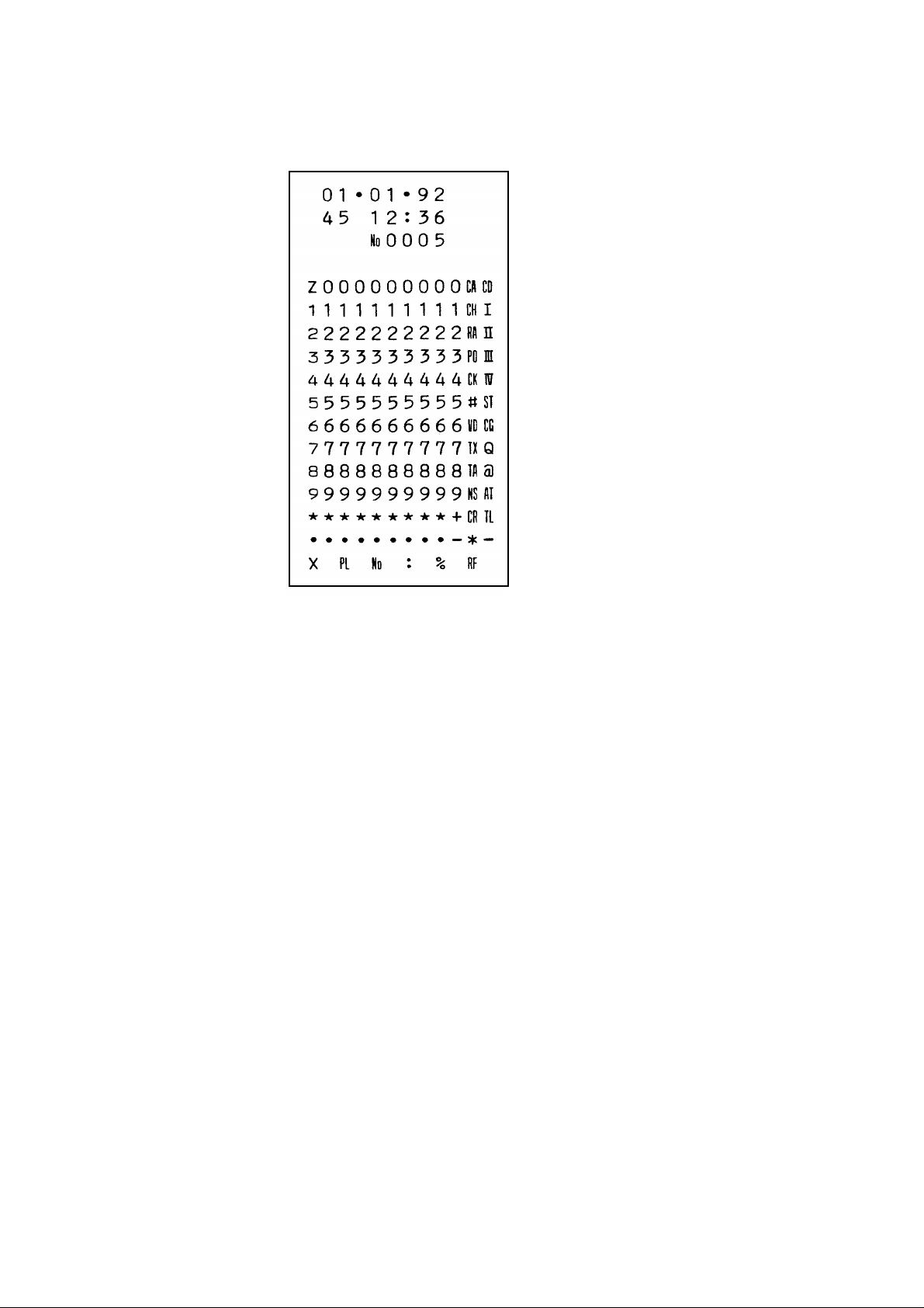
4-4-1. Display, RAM, drawer and printer check
Operation : 1 + ST
1) All segments turn on.
8 8 8 8 8. 8. 8. 8.
2) Date and time set
Set the following data in the machine automatically.
Date : 1st January, 1992
Time : 12:34:00
3) RAM write and read check
The machine writes data into RAM and read out the data to compare with written data.
When this check is finished correctly, the machine goes to check No. 4).
However, if an error is occurred, the machine sounds an error tone, prints the error receipt,
and stops Hard check program.
Error receipt sample " -- -- "
4) Drawer open check
Open the drawer.
5
Page 8
5) Printing check
Print the following character.
6) Receipt issue
The following receipt is issued.
7) Test display
Z 0 0 0 0 0 0 0 0 0 CA CD
7 6 5 4 3 2. 1 0
4-4-2. RAM read only check
Operation :5 + ST
Note : Be sure to execute the RAM write and read check (1 + ST) before this check.
The machine reads out the data to compare with written data until an error is occurred and
brinks " -- " on the display during this check.
To stop this check, turn the mode switch to OFF position.
If an error is occurred, the machine sounds an error tone, prints " -- -- " on the
receipt, and stops this check.
4-4-3. Voltage check of memory back-up battery
Operation :7 + ST
Display the voltage of back-up battery in real time. (Measurement is Volt (V) level.)
To stop this check, turn the mode switch to OFF position.
6
Page 9
4-4-4. All characters print check
Operation : 8 + ST
4-4-5. Display the time
Operation : 9 + ST
The machine display the time.
To stop this check, press the Clear key.
1 2 -- 3 4 01 The time counts up.
If you make following operation, the machine resets the time data and starts again.
Operation : 9 9 + ST
4-4-6. How to release the diagnostic mode
Execute MAC operation.
7
Page 10
5. OPTION CIRCUIT
Power protection battery B-6
Power protection battery B-6 os available fro CE-2350.
However, interface circuit is not mounted the machine.
When you use the B-6, mount the following parts.
Parts list for interface
Code No. Parts Name Specification Q’ty
2200 3577 Transistor 2SA1015(GR,O,Y) 1
2301 0011 Diode 1S2471 2
2310 3541 Zener diode RD12EB2 1
2600 7313 Carbon film resistor R-25-10K-J 3
2614 0552 Carbon film resistor R-25-2K-J 1
2801 7098 Electrolytic capacitor 50RE2 1
6219 4553 Connector fixing plate E311094-1 1
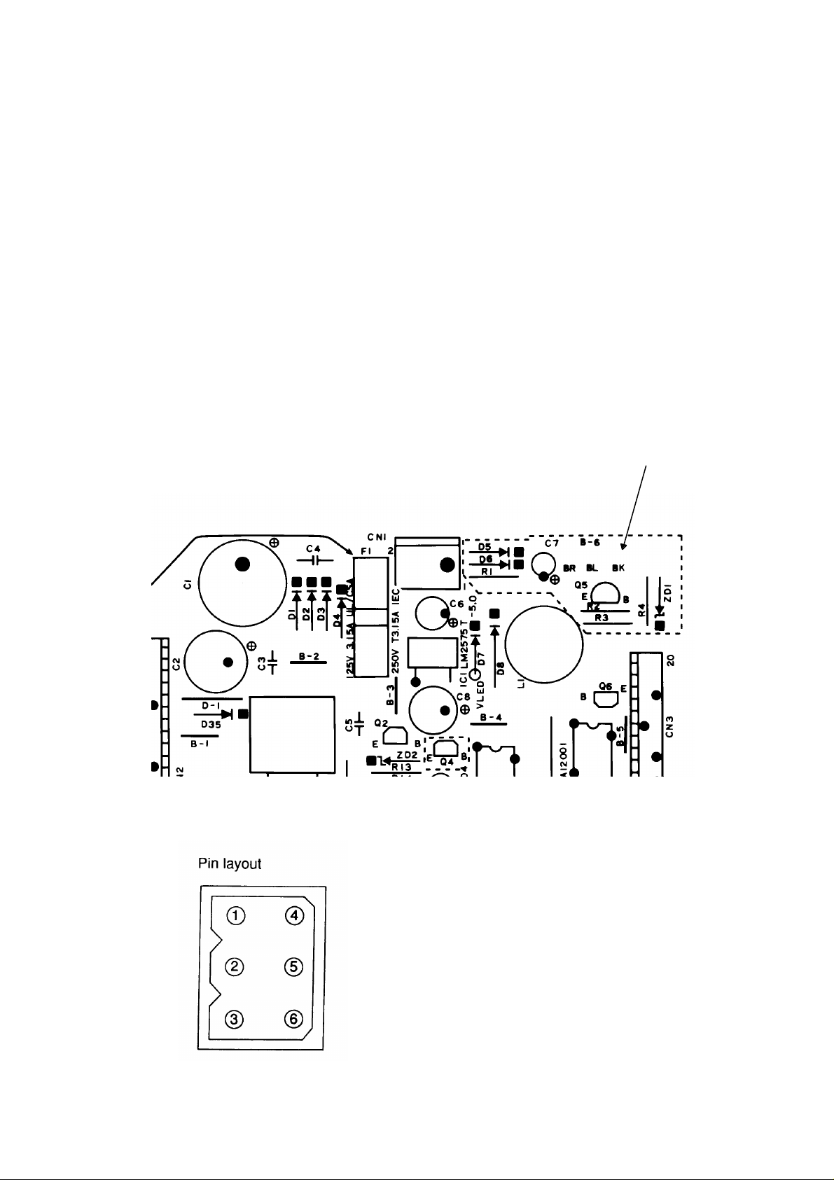
6236 6180 P1625-06P connector ass’y E314531B-10(#22-200) 1
Interface circuit for B-6
Pin assignment for B-6 connector
Pin No. Description
1 F.G. (Green)
2 Not used
3 CS (Black)
4 GND (Blue)
5 Not used
6 VP (Brown)
8
Page 11
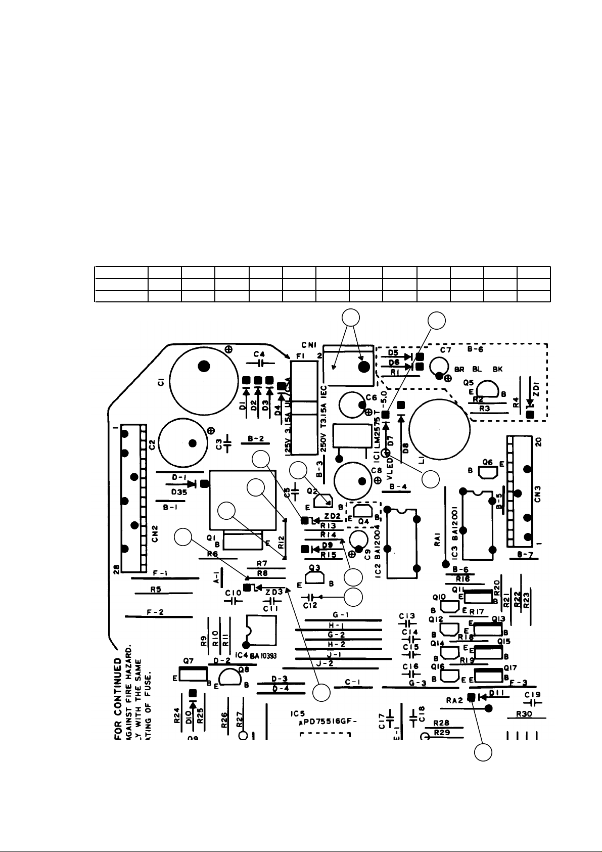
6. CIRCUIT EXPLANATION
3
4
6-1. Power supply circuit
2
1
5 7 8 9
10
11
12
6
Q1 : Transistor for controlling voltage (VP)
Q2 : Transistor for voltage detection
Q3 : Transistor for controlling power down (PWD) signal
ZD2 : Zener diode for controlling base current of Q2
ZD3 : Zener diode for detecting power down (PWD) signal
After plug the AC cord into the outlet, the AC voltage (23.8V) appears at CN1 connector.
Then this voltage is rectified by the diode brige and it become constant voltage through the capacitor C1.
[Voltage VP]
A constant voltage (31.4V) appears on the “ 2 “ position. This voltage made from the constant
voltage circuit consist of transistor Q1 and Q2, zener diode ZD2, resisror R7, R8, R12 and R13.
[Voltage VLED and VCC]
The voltage goes to pin No.1 of regurator IC1 and then it is out from pin No.2 of IC1 as stable
voltage (5.6V).
Then this voltage down to 5 volts through the diode.
It is used for VCC ( for logic) and VLED (for display drive).
Also, it goes to pin No.4 of IC1 and using to control the output voltage level.
Inductor L1 is used to stabilize the VCC voltage when the drawer opened.
9
Page 12
[PWD signal]
10
11
8
2
3
5
4
After plug the AC cord into outlet, VP voltage appears on the base terminal of transistor Q3.
When the VP exceeds 16 volts, Q3 is turned on by the differential voltage between base and
emitter terminal of transistor Q3.
Then the PWD signal goes to GND level and informes “ Power ON “ to the CPU.
When the VP drops less than 16 volts, Q3 is turned off.
Then the PWD goes high level since the PWD is pulled up to VDD.
When the CPU receives “ High “ signal of PWD, CPU goes to “ Power failure process “.
Note : During plug the Ac cord into outlet, all voltages are supplied to the PCB.
If you open the machine for repair, make sure plug off.
[Location for voltage check points]
Actual value on the E259-1 PCB (unitV)
Check point 1 2 3 4 5 6 7 8 9 10 11 12
Power ON 23.8(AC) 31.4 25.2 7.61 24 8.2 8.1 0.6 0 5 5.6 5
Power cord off 0 0 0 0 0 0 0 0 4 0 0 0
1
6
9
7
12
10
Page 13
6-2. CPU (uPD75516GF-351-3B9)
Pin No. Signal Descriptions In/Out
1 AN0 Mode switch signal (RF,OFF,REG,X,Z) signal In 2.0V
2 AVREF VCC terminal (+5V) - 5.0V
3 VDD VDD terminal (+5V) - 5.0V
4 VDD VDD terminal (+5V) - 5.0V
5 P113 Motor drive signal (M4) Out Low
6 P112 Motor drive signal (M3) Out High
7 P111 Motor drive signal (M2) Out Low
8 P110 Motor drive signal (M1) Out Low
9 P103 Stamp / Clock signal Out Low
10 P102 RAM address signal (A12) / Receipt and Journal feed (FEED) Out Low
11 P101 RAM address signal (A09/A11) / Head drive signal (HD6) Out Low
12 P100 RAM address signal (A08/A10) / Head drive signal (HD5) Out Low
13 P93 RAM address signal (A03/A07) / Head drive signal (HD4) Out Low
14 P92 RAM address signal (A02/A06) / Head drive signal (HD3) Out Low
15 P91 RAM address signal (A01/A05) / Head drive signal (HD2) Out Low
16 P90 RAM address signal (A00/A04) / Head drive signal (HD1) Out Low
17 SI1/P83 Key input signal (Ki7) In High
18 SO1/P82 Key input signal (Ki6) In High
19 SCK1/P81 Key input signal (Ki5) In High
20 PP0/P80 Key input signal (Ki4) In High
21 KR7/P73 Not used Out -
22 KR6/P72 Display segment signal (SG1) Out Pulse
23 KR5/P71 Display segment signal (SF1) Out Pulse
24 KR4/P70 Display segment signal (SE1) Out Pulse
25 KR3/P63 Display segment signal (SD1) Out Pulse
26 KR2/P62 Display segment signal (SC1) Out Pulse
27 KR1/P61 Display segment signal (SB1) Out Pulse
28 KR0/P60 Display segment signal (SA1) Out Pulse
29 P53 Display segment signal (SDP0) Out Pulse
30 P52 Display segment signal (SG0) Out Pulse
31 P51 Display segment signal (SF0) Out Pulse
32 P50 Display segment signal (SE0) Out Pulse
33 VSS GND terminal 34 P43 Display segment signal (SD0) Out Pulse
35 P42 Display segment signal (SC0) Out Pulse
36 P41 Display segment signal (SB0) Out Pulse
37 P40 Display segment signal (SA0) Out Pulse
38 P33 Display segment coomon signal (Dg4) Out Pulse
39 P32 Display segment coomon signal (Dg3) Out Pulse
40 P31 Display segment coomon signal (Dg2) Out Pulse
41 P30 Display segment coomon signal (Dg1) Out Pulse
42 P23/BUZ Buzzer signal Out Low
43 P22/PCL Motor drive signal (for paper feeding) Out Low
44 P21 Step motor common signal (for print wheel) Out High
45 P20/PT00 Drawer open signal (DW) Out Low
46 P13/TI0 Key input signal (Ki9) In High
47 P12/INT2 Key input signal (Ki8) In High
48 P11/INT1 Power down signal In Low
49 P10/INT0 Reset pulse from printer In High
50 P03/SI0/SB1 Key input signal (Ki3) In High
PW-ON
level
11
Page 14
Pin No. Signal Descriptions In/Out
51 P02/SO0/SB0 Key input signal (Ki2) In High
52 P01/SCK0_ Key input signal (Ki1) In High
53 P00/INT4 Key input signal (Ki0) In High
54 VSS GND terminal 55 XT1 Sub system clock signal (32.768KHz) In Pulse
56 XT2 Sub system clock signal (32.768KHz) In Pulse
57 IC GND terminal -
58 X1 Main system clock signal (4.19MHz) In Pulse
59 X2 Main system clock signal (4.19MHz) In Pulse
60 RESET_ Initilize signal In High
61 P143 RAM write enable signal (WE_) Out High
62 P142 RAM chip enable signal (CE_) Out High
63 P141 Journal feed common signal Out Low
64 P140 Receipt feed common signal Out Low
65 P133 RAM data signal (D3) In/Out High
66 P132 RAM data signal (D2) In/Out High
67 P131 RAM data signal (D1) In/Out High
68 P130 RAM data signal (D0) In/Out High
69 P123 Key common signal (Kc02) Out Pulse
70 P122 Key common signal (Kc01) Out Pulse
71 P121 Key common signal (Kc00) Out Pulse
72 P120 RAM address signal (A14) Out Low
73 AVSS GND terminal 74 P153/AN7 Receipt ON/OFF signal In High
75 P152/AN6 Motor error signal In Low
76 P151/AN5 Pad data signal (PAD2) In High
77 P150/AN4 Pad data signal (PAD1) In High
78 AN3 GND terminal -
79 AN2 Battery voltage detection terminal In 0~4.5V
80 AN1 Drawer sensor signal In Low
PW-ON
level
Note : The “PW-ON level” is measured under following conditions.
1) Mode switch is REG position.
2) The display is the time.
3) Receipt switch is ON position.
4) PAD1 and Pad2 are both open.
12
Page 15
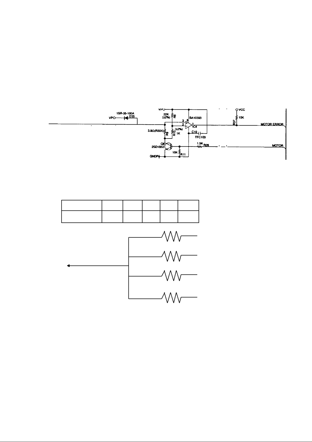
6-3. Motor error detection circuit
To Printer
To CPU
RF
REG
X
Z
16Kohms
6.2Kohms
2Kohms
560 ohms
To Pin No.1 of CPU
When the CPU output motor signal, transistor Q8 becomes on and the voltage level at “A” point
becomes GND. Then, paper feeding motor rotate. Normally, pin No.1 of IC4 appears low signal.
IC4 detects differential voltage between pin No.2 and 3.
In case pin No.3 is higher than No.2, output(Pin No.1) signal is hogh.
If motor happens over load ( Paper jam etc.), over load current (250mA) runs resistor R9.
So, “A” point voltage lebel becomes high.
Then IC4 outputs high signal and then CPU knows motor error occured.
When the CPU receives “Motor error signal”, CPU stops motor signal.
6-4. Mode key switch status read
The CPU knows the mode switch status by voltage level of pin No.1.
the voltage level is down by resistor. Each voltage is as shown below.
Mode REG X Z RF OFF
Voltage (V 196 3.29 4.36 0.98 0
13
Page 16

6-5. RAM address/head drive signal switching circuit
The CPU is used the port for RAM address (A0~A11) and head drive signal (HD1~HD6).
To select the RAM address and head drive signal, CPU use “STEP MOTOR COM” signal.
When CPU wants to read the RAM chips, CPU stops “STEP MOTOR COM” signal.
The CPU controls RAM address (A0~A12) using IC10 because of CPU has 7 ports.
First, CPU sneds RAM address (A4~A7,A10,A11) to IC10, and IC10 store the address data.
Next, CPU send RAM address (A0~A3,A8,A9,A12,A14) to RAM.
At the same time, CPU sendsclock signal to IC10.
Then, IC10 outputs stored data (A4~A7,A10,A11). In this way, CPU controls RAM address.
6-6. Initilize IC (Reset IC)
When the voltage level on pin No.60 of CPU is not sabilized, CPU does not work properly
in rare case.
Therefore, this machine uses the initilize IC for stabilizing the voltage.
Even the voltage level of VDD (Pin No.2) is changed of Initilize IC, initialize IC output stabilized
5 volts from pin No.1.
14
Page 17

6-7: Printer error condition of CPU
1). When motor error signal comes, CPU knows printer error.
2). When reset pulse does not come within a period of time which is controlled by CPU,
CPU knows printer error. Then CPU stops printing.
CPU selects printing character by software.
7. TO OPEN THE UPPER CASE
1. Remove the printer cover.
2. Remove the 4 pcs of screw No.1 near the printer unit.
3. Slide the upper case to backward and pull it up, and then remove it.
4. Remove the 5 pcs of screw No.2 to separate the keyboard.
15
Page 18

8. PCB LAYOUT
16
Page 19

- 17 -
Page 20

- 18 -
Page 21

- 19 -
Page 22

- 20 -
Page 23

- 21 -
Page 24

- 22 -
Page 25

- 23 -
Page 26

- 24 -
Page 27

- 25 -
Page 28

- 26 -
Page 29

- 27 -
Page 30

CONTENTS
1. Main PCB ass’y ............................................................................................................ 29
2. Main display block ........................................................................................................ 31
3. Customer display block ................................................................................................ 32
4. Keyboard block ........................................................................................................... 33
5. Button block ............................................................................................................... 34
6. Power supply block ..................................................................................................... 36
7. Upper case block ......................................................................................................... 37
8. Printer block/ Printer fixing block/Others......................................................................... 38
9. Printer unit ................................................................................................................... 40
PARTS LIST
MODEL : CE-2350 (EX-259)
10. Drawer ........................................................................................................................ 42
NOTES :
1. Price and specifications are subject to change withput prior notice.
2. As for spare parts order and supply, refer to the “GUIDEBOOK for Spare Parts Supply”,
published separately.
3. The numbers in item column corespond to the same numbers in drawing.
4. Remarks
N : New parts R : RANK
Q : Quantity used per unit A : Essential
* : Minimum order/supply quantity B : Stock recommended
C : Less recommended
X : No stock recommended
28
Page 31

1.Main PCB ass’y
FOB Japan
N Item Code No. Parts Name Specification Ver. Q M
MAIN PCB ASS'Y
N 6192 6210 Main PCB ass'y (E259-1) E211743*1 1 10720 A
IC11 2006 0717 LSI LC36256PLL10/12/15 1 630 A
N IC5 2006 1039 LSI UPD75516GF-585-3B9 1 750 A
IC13 2101 0189 MOS IC TC74HC138AP 1 65 A
IC10 2105 1071 C-MOS IC TC74HC174AP 1 70 A
IC4 2114 1512 Liner IC BA10393 1 5 34 A
IC7,8,9 2114 2436 Monolythic IC BA12003 3 75 A
IC2 2120 6741 Monolythic IC BA12004 1 74 A
IC1 2120 6823 Liner IC LM2575T-5.0/LB03 1 380 A
IC6 2120 6824 Monolythic IC STA471A 1 160 A
IC12 2120 7381 Reset IC S-80730AN-Z 1 60 A
IC3 2120 9181 Monolythic IC BA12001 1 85 A
Q7,11,13,15,17 2210 7309 Transistor 2SB1240V2-Q,R 5 20 26 B
Q2,3 2220 3746 Transistor 2SC4640(T,U)-AC 2 20 9 B
Q8,18 2230 4135 Transistor 2SD1853-AA 2 33 B
Q1 2230 5336 Transistor 2SD1196 1 5 96 B
N Q6 2250 1099 Digital transistor DTC113ZS-TP-T 1 5 52 B
Q9,10,12
Q14,16
D1~4,10
D27,35
D7,9,11~26
D28~34,36
ZD3 2310 6728 Zener Diode RD16EB3-TN-T 1 20 8 B
ZD4,5 2310 7229 Zener Diode RD24EB2-TN-T 2 8 B
ZD2 2310 9449 Zener Diode RD7.5EB3-TN-T 1 20 8 B
DA1 2310 9450 Shottky barrier diode SB007W03S-AC 1 27 B
D8 2310 9452 Shottky barrier diode RK-14V 1 43 B
X1 2520 3445 Crystal oscillator C-002RX(M90-76) 1 47 A
N R45~50 2652 1133 Carbon film resistor CR-25-1OHMJ-T 6 20 3 X
R16~19 2652 1140 Carbon film resistor CR-25-100OHMJ-T 4 10 25 X
R73 2652 1147 Carbon film resistor CR-25-150OHMJ-T 1 25 X
R40 2652 1154 Carbon film resistor CR-25-560OHMJ-T 1 10 25 X
R12 2652 1168 Carbon film resistor CR-25-1KOHMJ-T 4 10 25 X
N R10 2652 1175 Carbon film resistor CR-25-1KOHMG-T 1 20 3 X
N R26 2652 1182 Carbon film resistor CR-25-1.5KOHMJ-T 1 20 3 X
N R41,43 2652 1189 Carbon film resistor CR-25-2KOHMJ-T 2 20 3 X
N R13 2652 1196 Carbon film resistor CR-25-2.7KOHMJ-T 1 20 3 X
N R30,32~35
R51~53
R55~66 2652 1210 Carbon film resistor CR-25-4.7KOHMJ-T 12 10 25 X
N R8 2652 1217 Carbon film resistor CR-25-5.1KOHMJ-T 1 20 3 X
N R39 2652 1224 Carbon film resistor CR-25-6.2KOHMJ-T 1 20 3 X
N R69 2652 1231 Carbon film resistor CR-25-8.2KOHMJ-T 1 20 3 X
N R11,15,20~24
R31,36,37,44,68
R74~78
N R6 2652 1252 Carbon film resistor CR-25-22KOHMG-T 1 20 3 X
N R27,70,71,79 2652 1259 Carbon film resistor CR-25-56KOHMJ-T 4 20 3 X
R14,72 2652 1266 Carbon film resistor CR-25-100KOHMJ-T 2 10 25 X
R38 2652 1273 Carbon film resistor CR-25-330KOHMJ-T 1 10 25 X
N R54 2652 1280 Carbon film resistor CR-25-1MOHMJ-T 1 20 3 X
N R9 2652 1287 Carbon film resistor R50XT-08J3R9 1 20 28 X
N R7 2652 1392 Carbon film resistor R50XT-08J122 1 20 28 X
N R42 2652 2043 Carbon film resistor CR-25-16KOHM-J-T 1 20 3 X
R5 2700 3858 Metal film resistor CRH200-FH24-J-301 1 20 10 X
R67 2700 3859 Metal film resistor CRH100-FH11-J-6R8 1 10 7 X
RA2 2720 4236 Module resistor MS5635F 1 10 26 C
RA3,4 2720 4244 Module resistor MS5636F 2 10 26 C
RA1,5 2730 0021 Module resistor MS1038F 2 10 40 C
2259 0063 Digital transistor DTC114YS-TP-T 5 20 B
2301 0089 Diode 1SR35-100A-T-82-T 7 20 7 C
2301 0101 Diode 1S2473-T-77-T 26 20 8 C
2652 1203 Carbon film resistor CR-25-3.9KOHMJ-T 8 20 3 X
2652 1238 Carbon film resistor CR-25-10KOHMJ-T 17 20 3 X
N.R.Yen
Unit Price
R
29
Page 32

N Item Code No. Parts Name Specification Ver. Q M
X2 2801 8932 Ceramic oscillator CST4.19MGW 1 75 A
N C6 2807 2231 Electrolytic capacitor RE2-50V470M-T2 1 20 22 C
N C9 2807 2238 Electrolytic capacitor RE2-50V010M-T2 1 20 13 C
N C8 2807 2245 Electrolytic capacitor RE2-25V331M-T2 1 10 36 C
N C2 2807 2252 Electrolytic capacitor RE2-35V102M 1 110 C
N C1 2807 2259 Electrolytic capacitor RE3-50V332M 1 310 C
N C21 2807 2770 Ceramic capacitor HE40TJCH120J 1 20 10 X
N C13~18,32
C34~40
N C20 2818 3881 Ceramic capacitor HE40TJCH150J 1 20 10 X
N C43 2818 3882 Ceramic capacitor HE80TJYB472K 1 20 7 X
C33 2819 0735 Ceramic capacitor HE40TJYB471K 1 20 4 X
C25 2819 0743 Ceramic capacitor HE40TJYB101K 1 20 6 X
C3,5,11,12,19
C22~24,26~28
C31,42
C30,41 2820 3233 TF capacitor ECQ-V1H-104-JZW 2 22 X
C10,29,44 2820 3713 TF capacitor ECQ-B1H103KFW 3 20 7 X
C4 2830 5729 Mylar capacitor 50F2S563J 1 14 X
F1 3000 6559 Fuse 237 315 1 5 52 A
L1 3018 0854 Inductor MCDR1419-681K 1 5 52 X
BUZZER 3122 1589 Sounducer PKM22EPP-2002 1 65 C
CN5 3500 3355 Pin ass'y 3P IL-G-3P-S3T2-E 1 7 C
CN3 3500 5831 PCB connector 52045-2045 1 50 C
CN4 3500 7122 Pin ass'y 53253-0310 1 20 8 C
N CN2 3501 5460 FFC Connector 52045-2845 1 5 93 C
N CN6 3501 5474 FFC connector 52045-2245 1 5 78 C
CN1 3510 2680 Pin ass'y 2P 5277-02A 1 20 15 C
F2 3631 0328 Fuse UL-TSCR-0.8A 1 75 A
F1 3640 2331 Fuse clip UF-0033 2 10 8 X
N 4308 1067 PCB E259-1
2813 0217 Ceramic capacitor HE50TJYB102K 14 20 4 X
2819 5542 Ceramic capacitor HE12TJYB103K 13 10 X
3750 1272 Heat sink OSH-1625-SPL 1 70 X
E211747-1 1 310 X
(without components)
5041 5155 Screw (+) 3X8 ZMC-3 1 50 2 X
FOB Japan
N.R.Yen
Unit Price
R
30
Page 33

2. Main display block
1
3
5
2
4
6
N Item Code No. Parts Name Specification Ver. Q M
FOB Japan
N.R.Yen
Unit Price
R
MAIN DISPLAY BLOCK
6191 0091 E240-E2 ass'y E211153*1 1 3510 C
1 2320 1365 LED HDSP-5621#S02 4 160 A
N 2601 6816 Carbon film resistor ERD25TJ121V 8 20 3 X
N 2601 6817 Carbon film resistor ERDS2TJ121V 7 20 3 X
2 3500 5833 PCB connector 52044-2045 1 50 C
3 3500 5834 Pin ass'y 9P 53254-0910 1 30 C
4 3500 5835 Pin ass'y 11P 53254-1110 1 30 C
5 4306 1004 PCB E240-E2
(without components)
6 6221 3899 FFC joiner A E411354-4 1 140 A
E311067A-1 1 77 X
31
Page 34

3. Customer display block
10
11
7
8
9
12
N Item Code No. Parts Name Specification Ver. Q M
CUSTOMER DISPLAY BLOCK
6191 0092 E240-E2 ass'y E211153*2 1 3510 C
N 2601 6816 Carbon film resistor ERD25TJ121V 8 20 3 X
N 2601 6817 Carbon film resistor ERDS2TJ121V 7 20 3 X
7 2320 1365 LED HDSP-5621#S02 4 160 A
8 4306 1004 PCB E240-E2
(without components)
9 6191 0334 Display connector ass'y E311301*1 1 380 B
10 6221 4059 Blind sheet R E311214-1 1 20 18 X
11 6245 5470 Display case E210920B-1 1 200 X
12 6246 3170 Rear case B E210921B-2 1 180 C
E311067A-1 1 77 X
FOB Japan
N.R.Yen
Unit Price
R
32
Page 35

4. Keyboard block
21
16
14
18
19
17
15
13
20
N Item Code No. Parts Name Specification Ver. Q M
KEYBOARD BLOCK
N 13 3501 5474 FFC connector 52045-2245 1 5 78 A
N 15 4308 1074 PCB E241-E4
N 20 6246 4790 FFC joiner E412212-2 1 190 A
14 4306 1013 PCB E241-E3-2
(without components)
(without components)
16 6191 0102 Mode key switch ass'y E311288*1 1 300 C
17 6231 9577 PC joiner A E411356A-1 1 10 26 A
18 6231 9578 PC joiner B E411356A-2 1 20 10 A
19 6029 0326 Switch contact spring A4897C-1 1 10 3 C
5111 5760 Tapping screw (+) (for mode key) 2.6X8 ZMC-3.. 2 50 2 X
5112 0124 Screw with washer (for keyboard) 3X8 ZMC-3..... 6 20 5 X
21 6221 4758 Slide knob E311468-1 1 30 X
E311071A-1 1 10 43 X
E312009-1 1 380 C
FOB Japan
N.R.Yen
Unit Price
R
33
Page 36

5. Button block
2
42
32
30
27
35
26
33
37
28
34
31
29
36
40
42
44
40
25
24
43
22
41
34
23
39
38
Page 37

N Item Code No. Parts Name Specification Ver. Q M
BUTTON BLOCK
22 6221 0630 Coil spring A E411104-1 1 3 C
23 6221 0648 Coil spring B E411104-2 10 3 C
24 6221 3988 L cap E210964-1 1 23 C
25 6221 4025 S cap E311103-1 41 13 C
26 6221 4356 S button 5 E311116-3 1 47 C
27 6221 4360 S button 1 E311279-1 1 15 C
28 6221 4361 S button 2 E311279-2 1 15 C
29 6221 4362 S button 3 E311279-3 1 15 C
30 6221 4363 S button 4 E311279-4 1 15 C
31 6221 4364 S button 6 E311279-5 1 15 C
32 6221 4365 S button 7 E311279-6 1 15 C
33 6221 4366 S button 8 E311279-7 1 15 C
34 6221 4367 S button 9 E311279-8 1 15 C
35 6221 4368 S button 0 E311279-9 1 15 C
36 6221 4369 S button . E311279-10 1 15 C
37 6221 4370 S button 00 E311279-11 1 15 C
38 6221 4420 Spacer E311240-1 1 10 35 A
39 6221 4421 Common sheet E311241-1 1 80 A
N 6246 2000 Button filer S E412129-2 2 5 52 C
N 41 6246 3140 Button frame E110218B-1 1 370 X
N 42 6246 5470 Plate sub ass'y E312031A*1 U.S.A. 1 160 C
N 42 6246 5480 Plate sub ass'y E312031A*2 Canada 1 160 C
N 43 6246 7761 L button E210963A-3 1 10 29 C
N 44 6246 7803 S button E311101A-3 53 20 13 C
40 6221 5086 Contact rubber E411820-1 54 4 A
FOB Japan
N.R.Yen
Unit Price
R
35
Page 38

6. Power supply block
45
47
48
46
N Item Code No. Parts Name Specification Ver. Q M
POWER SUPPLY BLOCK
45 3000 3020 Power transformer TE-233-E4D 1 910 A
46 3030 4055 Ferrite core L5T18X6X10 1 45 X
47 3700 4281 Power cord PS204 1 400 C
48 5530 0526 Cable joiner CE2 2 10 9 X
FOB Japan
N.R.Yen
Unit Price
R
36
Page 39

7. Upper case block
56
58
55
54
57
52
50
51
53
37
49
Page 40

FOB Japan
N Item Code No. Parts Name Specification Ver. Q M
UPPER CASE BLOCK
5111 2714 Screw with washer 3X20 ZMC-3.. 2 20 5 X
5112 0124 Screw with washer 3X8 ZMC-3..... 5 20 5 X
49 6220 2505 Display bush E310377-1 1 5 63 X
50 6221 3884 Mode cover B E210953-2 1 180 C
51 6221 4061 Blind seal E311215-1 1 20 20 X
N 52 6246 3330 Display window A E210952A-10 1 200 B
N 53 6246 4740 Upper case E110216-10 1 850 X
54 6218 4957 Key set sub ass'y E44596A*1 1 180 B
6218 4965 OP key E44549-1 2 100 B
6218 4973 OW key E44549-3 2 100 B
N 55 6221 3878 Printer cover E110217-1 1 410 C
56 6216 1949 Paper cutter E42778-1 1 10 26 C
N 57 6246 4780 Name plate E412211-3 1 10 39 X
58 6221 3812 Name label E411379-1 1 16 X
N.R.Yen
Unit Price
8. Printer block / Printer fixing block / Others
71
R
59
70
60
69
67
64
62
63
66
65
61
68
38
Page 41

N Item Code No. Parts Name Specification Ver. Q M
PRINTER BLOCK
FOB Japan
N.R.Yen
Unit Price
R
N 59 1000 8141 Printer unit CR-710-001MA 1 7360 A
N 60 6191 0077 FG wire ass'y E411673*1 1 5 85 X
N 65 6191 0080 Lead wire ass'y E411694*1 1 20 22 C
N 66 6191 0081 Connector ass'y E411695*1 1 10 42 C
N 5440 0196 Screw 3X8.ZMC-3 1 20 3 X
N 5111 2716 Screw with washer 3X32 ZMC-3 1 20 10 X
N 5150 1631 Washer 6.6XØ17X1.2 ZMC-3 1 20 16 X
5150 1637 Screw 4X8 ZMC-3... 1 20 5 X
PRINTER FIXING BLOCK
61 6000 6091 Battery spring G67 A43656-1 1 10 5 C
62 6001 0862 Battery spring B-1 P408-1 1 10 23 C
63 6001 0871 Battery spring B-2 P409-1 1 10 23 C
64 6322 4499 Battery spring A A42606-1 1 10 10 C
67 6221 4762 Paper roller E411696-1 2 10 18 C
68 6231 9641 Printer fixing stand E210951A-1 1 290 X
69 6221 3888 Battery cover E311096-1 1 10 38 B
70 6221 4069 Printer earth plate E411500-1 1 5 73 X
OTHERS
71 6221 3886 V/B connector fixing plate E311094-1 1 5 65 X
5112 0043 Screw with washer 3X8 ZMC-3 9 3 X
5112 0132 Screw with washer 3X10 ZMC-3... 1 2 X
5550 1424 locking spacer SPLS-8 5 20 11 X
5900 0419 Washer 4 2 20 5 X
5112 0035 Screw with washer 4X6 ZMC-3 3 20 6 X
5112 0043 Screw with washer 3X8 ZMC-3 2 3 X
5900 0419 Washer 4 3 20 5 X
39
Page 42

9. Printer unit
40
Page 43

N Item Code No. Parts Name Specification Ver. Q M
101 1909 1665 Derent pawl ass'y F750003000 1 100 X
102 1909 1666 Board ass'y A F750004000 1 530 X
104 1909 1667 Paper guide ass'y F750006000 1 650 B
105 1909 1668 Paper feed motor F750005020 1 930 A
106 1909 1669 First reduction gear F750005030 1 10 38 A
107 1909 1670 Printer cover F750005040 1 120 X
108 1909 1671 Ink roll spring F750005050 2 10 25 X
109 1909 1672 Paper inlet roller F750005060 2 5 63 X
110 1903 0733 C.T.B. screw M2.5 x 8 B012601011 3 50 12 X
111 1909 1673 Outside toothed lock washer M2.6 B090650112 2 20 3 X
112 1908 5554 C.C.S. screw M3 x 5 B300304111 1 20 12 X
113 1903 0632 C.B.screw M3 x 4 B010350111 2 50 6 X
114 1909 1674 C.T.B. screw 3 x 6 B013001611 2 20 15 X
115 1909 1675 R detector ass'y F750055000 1 160 A
116 1909 1676 Typeface sheet receptocle ass'y C M751001020 1 2160 A
117 1909 1677 Typeface motor print ass'y A F750651000 1 2380 A
118 1909 1678 Paper feed trigger ass'y F750252000 1 790 X
119 1909 1679 Paper feed shaft ass'y F750254000 1 730 A
120 1909 1680 Paper hold roller shaft ass'y F750255000 1 200 X
121 1903 0140 Paper feeding shaft holder F701252020 2 26 X
122 1909 1681 Paper feed gear F750251010 1 5 50 A
123 1909 1682 Paper feed frame F750251020 1 160 X
124 1909 1683 Paper hold spring F750251030 2 10 25 X
125 1909 1684 No.1 stamp drive lever F750251040 1 5 50 X
126 1909 1674 C.T.B. screw 3x 6 B013001611 1 20 15 X
127 1903 0788 Retaining ring Type-E (5) B150300811 1 50 2 X
128 1909 1685 Take-up frame sub ass'y F751303000 1 450 X
129 1909 1686 Second reduction gear A F750302010 1 5 50 C
130 1909 1687 Second reduction gear B F750302020 1 5 88 C
131 1909 1688 Paper take-up drive gear F750302030 1 10 38 C
132 1909 1689 Roller torque spring F750302040 1 110 X
133 1909 1690 Paper take-up drive pulley F750302050 1 10 38 C
134 1903 0787 Retaining ring Type-E(3) B150300611 2 50 2 X
135 1903 0177 Paper roller shaft F703301010 1 315 X
136 1909 1691 Paper take-up belt F244307030 1 180 C
137 1908 5554 C.C.S. screw M3 x 5 B300304111 2 20 12 X
138 1909 1692 Stamp force adjustment spring F750451010 1 20 24 X
139 1909 1693 No.2 stamp drive lever F750451020 1 100 X
140 1909 1624 Stamp lever F240251020 1 110 X
141 1909 1694 Stamp return spring F750451030 1 20 18 X
FOB Japan
N.R.Yen
Unit Price
R
41
Page 44

10. Drawer unit
10-1. DL-2417 ( for U.S.A.)
42
Page 45

FOB Japan
N Item Code No. Parts Name Specification M Q
DL-2416 (U.S.A.)
201 6246 5070 Box sub ass'y E311975*1 1 1 4,330 X
203 6192 6330 Drawer ass'y E311955*2 1 1 2,890 C
202 6246 5140 Drawer label DL-2416 E311977-4 50 1 22 X
240 6221 4893 Rubber foot ZD01013-A 5 4 50 X
239 5150 1645 Screw with washer 3X5 ZMC-3... 50 10 6 C
238 5150 1644 Screw with washer 4X16 ZMC-3... 50 4 6 C
209 6246 4950 Drawer sub ass'y E311927*1 1 1 2,890 C
206 5301 5018 Washer 6X13X1 ZMC-3 50 2 2 X
204 5150 1652 Tapping screw (+) 3.5X8 ZMC-3 50 2 5 X
205 5200 0106 Rivet 5X30 50 1 10 X
207 5800 0043 Roller DR-19B-1.0 5 2 80 B
212 6246 5030 Earth spring E412092-1 50 1 13 X
213 6246 4860 Front panel E211607-2 1 1 190 X
208 6221 4900 Cylinder lock ZD20025 1 1 300 C
214 6192 6350 Bill/Coin case ass'y E110387*2 1 1 4,330 C
218 6221 4911 Partition plate ZD43652 1 4 330 B
216 6221 4902 Bill holder ZD18931 50 5 47 A
217 6221 4909 Bill/Coin case ZD43651 1 1 1,300 C
219 6246 5220 Bill holder spring E412160-1 1 5 170 A
220 6246 5240 Bill holder fixing plate E211621-1 1 1 200 C
215 5860 0679 Tapping screw (+) 3X8 ZMC-3 50 3 6 X
6192 6287 Bottom plate ass'y E211678*7 1 1 5,360 C
236 6246 4900 Bottom plate E211623-1 1 1 910 X
237 6246 5040 Damper rubber E412117-1 50 4 16 X
225 5500 0619 Roller DR-19B1 5 2 75 A
223 5150 1643 Hexagonal nut 6... 50 2 6 X
224 5301 5018 Flat washer 6X13X1 ZMC-3 50 2 2 X
222 5112 0035 Screw with washer 4X6 ZMC-3 50 2 6 X
N.R. Yen
Unit Price
R
226 6192 6317 Lock ass'y E211680*5 1 1 1,450 C
231 6246 4890 Lock fixing stand E211622-1 1 1 120 X
234 6246 5020 Hook lever shaft E412071-1 50 1 40 X
232 6246 4940 Hook lever E311876-1 5 1 65 X
233 6246 5010 Push spring E412069-1 50 1 16 C
230 5580 1461 Lock spring ZD03441-A 50 1 15 C
228 5161 5123 Screw (+) 3X8 ZMC-3 50 2 2 X
229 5440 0224 Screw with washer 4X14 ZMC-3 50 1 13 X
3000 7231 Micro switch V-103-1A5 1 1 560 C
5150 1649 Screw with washer 3X16 ZMC-3 50 1 10 C
43
Page 46

10-2. DL-2351 ( for Canada)
44
Page 47

N Item Code No. Parts Name Specification M Q
DL-2351 (Canada)
301 6246 5070 Box sub ass'y E311975*1 1 1 4,330 X
303 6192 6330 Drawer ass'y E311955*2 1 1 2,890 C
302 6246 5150 Drawer label DL-2351 E311977-5 50 1 22 X
340 6221 4893 Rubber foot ZD01013-A 5 4 50 X
339 5150 1645 Screw with washer 3 X 5 ZMC-3... 50 10 6 C
338 5150 1644 Screw with washer 4 X 16 ZMC-3... 50 4 6 C
309 6246 4950 Drawer sub ass'y E311927*1 1 1 2,890 C
306 5301 5018 Washer 6X13X1 ZMC-3 50 2 2 X
304 5150 1652 Tapping screw (+) 3.5X8 ZMC-3 50 2 5 X
305 5200 0106 Rivet 5X30 50 1 10 X
307 5800 0043 Roller DR-19B-1.0 5 2 80 B
312 6246 5030 Earth spring E412092-1 50 1 13 X
313 6246 4860 Front panel E211607-2 1 1 190 X
308 6221 4900 Cylinder lock ZD20025 1 1 300 C
314 6192 6340 Bill/Coin case ass'y E110387*1 1 1 4,330 C
315 5860 0679 Tapping screw (+) 3X8 ZMC-3 50 3 6 X
316 6221 4902 Bill holder ZD18931 50 4 47 A
317 6221 4909 Bill coin case ZD43651 1 1 1,300 C
318 6221 4911 Partition plate ZD43652 1 3 330 B
319 6246 5220 Bill holder spring E412160-1 1 4 170 A
320 6246 5230 Bill holder fixing plate E221620-1 1 1 200 C
6192 6287 Bottom plate ass'y E211678*7 1 1 5,360 C
336 6246 4900 Bottom plate E211623-1 1 1 910 X
337 6246 5040 Damper rubber E412117-1 50 4 16 X
325 5500 0619 Roller DR-19B1 5 2 75 A
323 5150 1643 Hexagonal nut 6... 50 2 6 X
324 5301 5018 Flat washer 6X13X1 ZMC-3 50 2 2 X
322 5112 0035 Screw with washer 4X6 ZMC-3 50 2 6 X
FOB Japan
N.R. Yen
Unit Price
R
326 6192 6317 Lock ass'y E211680*5 1 1 1,450 C
331 6246 4890 Lock fixing stand E211622-1 1 1 120 X
334 6246 5020 Hook lever shaft E412071-1 50 1 39 X
332 6246 4940 Hook lever E311876-1 5 1 65 X
333 6246 5010 Push spring E412069-1 50 1 16 C
330 5580 1461 Lock spring ZD03441-A 50 1 15 C
328 5161 5123 Screw (+) 3X8 ZMC-3 50 2 2 X
329 5440 0224 Screw with washer 4X14 ZMC-3 50 1 13 X
3000 7231 Micro switch V-103-1A5 1 1 560 C
5150 1649 Screw with washer 3X16 ZMC-3 50 1 10 C
45
 Loading...