

Page 1
Hardware Data Sheet
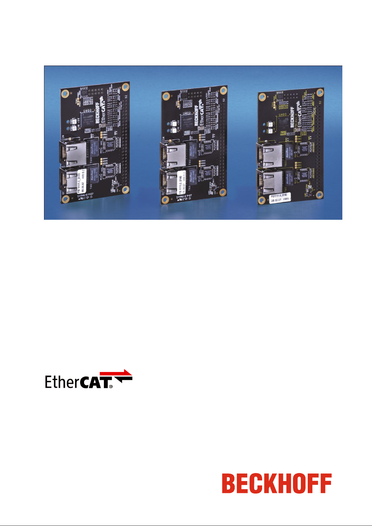
FB1111-0140
FB1111-0141
FB1111-0142
Piggyback Controller
Boards
Version 2.2
Date: 2011-12-04
Page 2

CONTENTS
CONTENTS
1 Foreword 1
1.1 Notes on the Documentation 1
1.1.1 Liability Conditions 1
1.2 Safety Instructions 1
1.2.1 Safety Rules 1
1.2.2 State at Delivery 1
1.2.3 Personnel Qualification 1
1.2.4 Description of Safety Symbols 1
1.3 Documentation Issue Status 2
2 Overview 3
2.1 Indicator LEDs 3
2.2 Variant Differentiation 3
3 Process Data Interfaces 4
3.1 PDI Configuration 4
3.2 Power Supply 6
3.3 Pinout 6
3.4 Using the FB1111-0142 in SPI- or µC-Mode 8
4 Component Placement Specification 10
4.1 Placed/Unplaced Components 10
4.2 Power Test Pads 10
4.3 FB1111-0142 – 32 bit In/Out digital Interface 11
4.3.1 Top Side of FB1111-0142 11
4.3.2 Bottom side of FB1111-0142 12
4.4 FB1111-0141 – Serial Peripheral Interface 13
4.4.1 Top side of FB1111-0141 13
4.4.2 Bottom side of FB1111-0141 14
4.5 FB1111-0140 – 8/16 bit asynchronous Microcontroller Interface 15
4.5.1 Top side of FB1111-0140 15
4.5.2 Bottom side of FB1111-0140 16
5 Interfacing with the EL9820 Evaluation Kit 17
5.1.1 Left side pin header definition 18
5.2 EL9820 stacking examples 19
6 Electrical Specification 20
6.1 Ratings 20
6.2 EMC – Electro magnetic compatibility 20
7 Mechanical Specification 21
7.1 Board Dimensions 21
7.2 Physical Connector Specification 22
7.3 Recommended Panel Opening 22
II FB1111 Piggyback Controller Board
Page 3
CONTENTS
7.4 Top/Bottom Side Component Height Definition 23
8 Appendix 25
8.1 Support and Service 25
8.1.1 Beckhoff’s branch offices and representatives 25
8.2 Beckhoff Headquarters 25
FB1111 Piggyback Controller Board III
Page 4

TABLES
TABLES
Table 1: Indicator LEDs ........................................................................................................................... 3
Table 2: Variants of the FB1111-014X .................................................................................................... 3
Table 3: Process data interfaces in combination with the EL9803.......................................................... 4
Table 4: Resistors for PDI Mapping ........................................................................................................ 4
Table 5: Networks for PDI Mapping ........................................................................................................ 5
Table 6: Pinout for different PDI Configurations ...................................................................................... 6
Table 7 Pinout of the FB1111-0142 in SPI and µC Mode ....................................................................... 8
Table 8: Power Test Pads ..................................................................................................................... 10
Table 9 Pin description of 8 pin right angle header ............................................................................... 18
Table 10: Typical Ratings ...................................................................................................................... 20
IV FB1111 Piggyback Controller Board
Page 5

FIGURES
FIGURES
Figure 1: Overview of the FB1111-014X ................................................................................................. 3
Figure 2: PDI Connector Power Pin Distribution ..................................................................................... 6
Figure 3: Example for placed/unplaced components ............................................................................ 10
Figure 4: Pads of resistor networks and single resistors ....................................................................... 10
Figure 5: EL9803 Adapter board – Top Side ......................................................................................... 17
Figure 6: EL9803 Adapter board – Bottom Side ................................................................................... 18
Figure 7: Left side right angle header pinout ......................................................................................... 18
Figure 8: Microcontroller Configuration with EL9803 ............................................................................ 19
Figure 9: SPI Configuration with EL9803 .............................................................................................. 19
Figure 10: Connection to GND-Earth .................................................................................................... 20
Figure 11: Board dimensions of the FB1111 – Top View ...................................................................... 21
Figure 12: Recommended Panel Opening ............................................................................................ 22
Figure 13: Component height zones for the top side of FB1111-014X ................................................. 23
Figure 14: Component height zones for the bottom side of FB1111-014X ........................................... 24
FB1111 Piggyback Controller Board V
Page 6

ABBREVIATIONS
µController
Microcontroller
as.
Asynchronous
DC
Direct Current
EEPROM
Electrically Erasable Programmable Read Only Memory. Non-volatile memory used
to store ESC configuration and description.
ESC
EtherCAT Slave Controller
EtherCAT
Real-time Standard for Industrial Ethernet Control Automation Technology
GND-Earth
Ground-Earth
LED
Light Emitting Diode, used as an indicator
PCB
Printed Circuit Board
PDI
Process Data interface
SPI
Serial Peripheral Interface
RJ45
FCC Registered Jack, standard Ethernet connector (8P8C)
ABBREVIATIONS
VI FB1111 Piggyback Controller Board
Page 7
Foreword
Danger
This symbol is intended to highlight risks for the life or health of personnel.
Warning
This symbol is intended to highlight risks for equipment, materials or the environment.
Note
This symbol indicates information that contributes to better understanding.
1 Foreword
1.1 Notes on the Documentation
This description is only intended for the use of trained specialists in control and automation engineering who are familiar with the applicable national standards. It is essential that the following notes and
explanations are followed when installing and commissioning these components.
1.1.1 Liability Conditions
The responsible staff must ensure that the application or use of the products described satisfy all the
requirements for safety, including all the relevant laws, regulations, guidelines and standards.
The documentation has been prepared with care. The products described are, however, constantly
under development. For that reason the documentation is not in every case checked for consistency
with performance data, standards or other characteristics. None of the statements of this manual represents a guarantee (Garantie) in the meaning of § 443 BGB of the German Civil Code or a statement
about the contractually expected fitness for a particular purpose in the meaning of § 434 par. 1 sentence 1 BGB. In the event that it contains technical or editorial errors, we retain the right to make alterations at any time and without warning. No claims for the modification of products that have already
been supplied may be made on the basis of the data, diagrams and descriptions in this documentation.
© This documentation is copyrighted. Any reproduction or third party use of this publication, whether in
whole or in part, without the written permission of Beckhoff Automation GmbH, is forbidden.
1.2 Safety Instructions
1.2.1 Safety Rules
The responsible staff must ensure that the application or use of the products described satisfy all the
requirements for safety, including all the relevant laws, regulations, guidelines and standards.
1.2.2 State at Delivery
All the components are supplied in particular hardware and software configurations appropriate for the
application. Modifications to hardware or software configurations other than those described in the
documentation are not permitted, and nullify the liability of Beckhoff Automation GmbH.
1.2.3 Personnel Qualification
This description is only intended for the use of trained specialists in control and automation engineering who are familiar with the applicable national standards.
1.2.4 Description of Safety Symbols
The following safety symbols are used in this operating manual. They are intended to alert the reader
to the associated safety instructions.
FB1111 Piggyback Controller Board 1
Page 8
Foreword
Version
Comment
0.1
First Version
0.2
Figure for PDI Connector supply added
PDI-Pinout checked and modified
Section for electrostatic protection added
Figures of component placement updated.
0.3
Description of EL9803 added
Figures illustrating component heights added
0.4
Foreword added
Format corrections
0.5
Corrections in figures
0.6
Errors in sections 4 removed
1.0
First official release
1.1
Modification of component height values in chapter 7.4
1.2
Dimension added in Figure 10
1.3
Table added in chapter 3
Figure added in chapter 4
Modifications in chapter 5
1.4
Operating- and storage temperature recommendations
1.5
EEPROM reprogramming information added in chapter 3
1.6
R525 changed to “placed” for SPI-PDI in Table 4
1.7
1.8
Comment in chapter 3 concerning EL9800_A
1.9
CPU_CLK_IN signal for synchronous µ-Controller interface in Table 6 added
2.0
PIN 30 changed to D[9] in Table 6
2.1
Pinout of FB1111-0142 in SPI- and µC-Mode added
2.2
Ethernet PHYs changed.
1.3 Documentation Issue Status
2 FB1111 Piggyback Controller Board
Page 9
Overview
IN
TR 0
ET1100
+5VRUN
Port 0
E²P
Link 1 Link 0
PHY
0
PDI Configuration
Area
PDI Connector
OUT
TR 1
Port 1
PHY
1
LED
Comment
+5V
Indicates 5V power supply
RUN
RUN indicator (LED) for application state
Link 0
Link/Act Indicator (LED) for port 0
Link 1
Link/Act Indicator (LED) for port 1
Product Code
Sub Code
PDI Interface
Comment
FB1111
0140
µController
16/8 bit asynchronous Microcontroller Interface
FB1111
0141
SPI
Serial Peripheral Interface (Slave)
FB1111
0142
Digital IO
32 bit In/Out digital interface
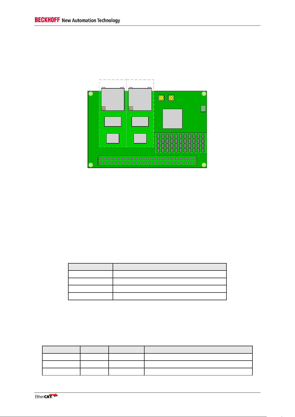
2 Overview
The EtherCAT Piggyback controller boards FB1111-014X combine an ET1100 EtherCAT Slave Controller, two EtherCAT ports and a PDI-Connector on a printed circuit board. The Piggyback controller
boards can as well be used for EtherCAT evaluation purposes as assembled into customer end products. Three variants with different Process Data Interfaces (PDIs) are existing in order to cooperate
with the most commonly known hardware interfaces like digital IO, SPI and Microcontroller.
Figure 1: Overview of the FB1111-014X
The board is structured in areas for Port 0 and Port 1, the PDI Connector, a PDI Configuration Area,
EEPROM, LEDs, and the ET1100 EtherCAT Slave Controller. While the EtherCAT port configuration,
LEDs, ET1100 and EEPROM are identical for the different variants of the FB1111-014X, the PDI Configuration Area differs in order to achieve different PDI Connector pinouts. Each EtherCAT port in Figure 1 combines a PHY, magnetics and an RJ45 connector. The PDI Configuration Area is a field of
resistors. Different pinouts on the PDI connector can be achieved by different resistor combinations in
this area. (See chapter 3.)
2.1 Indicator LEDs
Four LEDs for information about the device status are available on all three variants of the FB1111.
Table 1 is giving an overview over the indicator LEDs on the PCB.
Table 1: Indicator LEDs
2.2 Variant Differentiation
The three variants of the FB1111-014X are corresponding to three different PDI configurations. The
type of PDI interface can be identified by the last position in the product code. In Table 2 the variants
of the FB1111-014X are listed with respect to the different PDI interfaces.
FB1111 Piggyback Controller Board 3
Table 2: Variants of the FB1111-014X
Page 10
Process Data Interfaces
Piggyback Variant
Digital IO
µ-Controller
SPI
FB1111-0140
X
FB1111-0141
X
FB1111-0142
X
FB1111-0142
with EL9803 in
µC-Position
FB1111-0142
with EL9803 in
SPI-Position
Designator
Value
Footprint
0142 - 32bit Digital IO
0141 - SPI
0140 - 16bit as. µC
R500
0R
0603 X X R501
4.7k
0603 X R502
0R
0603 X
R503
4.7k
0603 X R504
0R
0603 X X R505
4.7k
0603
X
R506
0R
0603 X
R507
0R
0603 X X R508
0R
0603
X
R509
0R
0603 X R510
0R
0603 X
R511
0R
0603
X
R512
0R
0603 X R513
0R
0603
X
R514
0R
0603 X
X
Note
Usage of the EL9803 adaptor board becomes obsolete, if the FB1111-014X is
used in combination with the EL9800_4A evaluation board.
3 Process Data Interfaces
The Process Data Interface is used to communicate with external hardware. The printed circuit board
of the FB1111 supports three different PDI configurations. Thus the FB1111-0142 can be converted
into the FB1111-0140 and FB1111-0141 by replacing resistors in the PDI Configuration Area. As the
EL9820 Evaluation Kit contains the EL9803 adapter board, manual modification of the FB1111-0142 is
unnecessary. Using the EL9803, the SPI and µ-Controller interfaces can be realized without modifying
the FB1111-0142 piggyback controller board. Anyhow for in system testing manual modification of the
PDI Configuration Area may be necessary. Therefore in chapter 0 resistor mapping is listed. According to this mapping the signal pinout on the process data interface connector is shown in chapter 3.3.
Table 3 gives an overview about the FB1111-014X and EL9803 combinations. In chapter 5 detailed
information about the usage of the EL9803 in combination with the FB1111-0142 piggyback controller
board is given.
Table 3: Process data interfaces in combination with the EL9803
The Process Data Interface can be changed by reprogramming the EtherCAT configuration EEPROM
using TwinCAT.
3.1 PDI Configuration
Table 4 and Table 5 are showing the resistor and resistor network configuration for the different PDI
interfaces. Additionally to the designator (first column) the value (second column) and the footprint of
the desired resistor (third column) are listed. In the following columns a “X” is set, if the associated
resistor has to be placed on the PCB.
Table 4: Resistors for PDI Mapping
4 FB1111 Piggyback Controller Board
Page 11
Process Data Interfaces
Designator
Value
Footprint
0142 - 32bit Digital IO
0141 - SPI
0140 - 16bit as. µC
R515
0R
0603 X R516
0R
0603 X R517
0R
0603 X
X
R518
0R
0603 X R519
0R
0603 X R520
0R
0603 X
R521
0R
0603 X X R522
0R
0603 X R523
0R
0603
X
R524
0R
0603 X R525
0R
0603 X X R526
0R
0603
X
R527
0R
0603 X R528
0R
0603 X R529
0R
0603 X
R530
0R
0603 X R531
4.7k
0603
X
Designator
Value
Footprint
0142 - 32bit Digital IO
0141 - SPI
0140 - 16bit as. µC
RN500
4Y0R
1206 X RN501
4Y0R
1206 X RN502
4Y0R
1206 X
RN503
4Y0R
1206 X RN504
4Y0R
1206 X RN505
4Y0R
1206 X
RN506
4Y0R
1206 X RN507
4Y0R
1206 X X RN508
4Y0R
1206 X
X
RN509
4Y0R
1206 X X RN510
4Y0R
1206 X
X
RN511
4Y0R
1206 X X RN512
4Y0R
1206 X X RN513
4Y0R
1206 X
Note
4Y0R refers to a network of four independent resistors with 0R resistance. For
example resistors from PHYCOMP of the type ARV241 1206 0R can be used.
Warning
Incorrect modification of the resistor configuration can cause serious damage to
the FB1111 EtherCAT piggyback controller board. Modification of the PDI Configuration is on the users own risk and therefore not covered by warranty.
Table 5: Networks for PDI Mapping
FB1111 Piggyback Controller Board 5
Page 12

Process Data Interfaces
1
10
19
28
37
46
47 49
50
PHY 1 PHY 0
PDI Configuration Area
VCC (5V)
+3.3V
GND
1 Pin Number
Pin number
Port
0142 - 32bit Digital IO
0141 - SPI
0140 - 16bit as. µC
1
GND
2
PA0
I/O[0]
GPI[6]
A[0]
3
PA1
I/O[1]
GPI[5]
A[1]
4
PA2
I/O[2]
GPI[4]
A[2]
5
PA3
I/O[3]
GPO[7]
A[3]
6
PA4
I/O[4]
GPO[6]
A[4]
7
PA5
I/O[5]
GPO[5]
A[5]
8
PA6
I/O[6]
GPO[4]
A[6]
9
PA7
I/O[7]
GPI[3]
A[7]
10
GND
11
PB0
I/O[8]
GPI[2]
A[8]
12
PB1
I/O[9]
GPI[1]
A[9]
13
PB2
I/O[10]
GPI[0]
A[10]
14
PB3
I/O[11]
GPO[3]
A[11]
15
PB4
I/O[12]
GPO[2]
A[12]
16
PB5
I/O[13]
EEPROM Loaded
17
PB6
I/O[14]
GPO[1]
A[13]
18
PB7
I/O[15]
GPI[11]
CPU_CLK_IN
3.2 Power Supply
Figure 2 shows the distribution of the power pins on the PDI Connector from top side view.
Figure 2: PDI Connector Power Pin Distribution
The Pins 47 and 49 have to be supplied with +5V V
Pin 50 is a 3.3V Output from one DC-DC con-
CC.
verter on the FB1111-014X. The power supply on the FB1111-014X is divided in two sections. One
converter is supplying the PHYs for port 0 and 1. The second DC-DC converter supplies the ET1100
ASIC and all other parts on the printed circuit board. In consequence, the maximum current that can
be driven through the 3.3V output (Pin 50) is limited to 100mA. The GND pins, which are marked blue,
have to be connected to a ground plane on the supplying PCB. All in- and outputs are 3.3V compatible. Applying higher voltages will cause serious damage to the device.
3.3 Pinout
Table 6: Pinout for different PDI Configurations
6 FB1111 Piggyback Controller Board
Page 13

Process Data Interfaces
Pin number
Port
0142 - 32bit Digital IO
0141 - SPI
0140 - 16bit as. µC
19
GND
20
PC0
I/O[16]
GPI[7]
D[0]
21
PC1
I/O[17]
GPO[8]
D[1]
22
PC2
I/O[18]
SPI_SEL
D[2]
23
PC3
I/O[19]
GPO[10]
D[3]
24
PC4
I/O[20]
GPO[11]
D[4]
25
PC5
I/O[21]
GPI[8]
D[5]
26
PC6
I/O[22]
SPI_INT
D[6]
27
PC7
I/O[23]
GPI[10]
D[7]
28
GND
29
PD0
I/O[24]
SPI_D_IN
D[8]
30
PD1
I/O[25]
GPO[13]
D[9]
31
PD2
I/O[26]
SPI_D_OUT
D[10]
32
PD3
I/O[27]
GPO[15]
D[11]
33
PD4
I/O[28]
GPI[12]
D[12]
34
PD5
I/O[29]
GPI[13]
D[13]
35
PD6
I/O[30]
GPI[14]
D[14]
36
PD7
I/O[31]
GPI[15]
D[15]
37
GND
38
PE0
WD_TRIGGER
SPI_CLK
nCS
39
PE1
OUT_VALID
N.C.
nRD
40
PE2
SOF
N.C.
nWR
41
PE3
N.C.
N.C.
nBHE
42
PE4
SYNC[0]/LATCH[0]
43
PE5
SYNC[1]/LATCH[1]
44
PE6
LATCH_IN
N.C.
nINT
45
PE7
OE
N.C.
nBUSY
46
GND
47
VCC
48
N.C.
49
VCC (5V Input)
50
3.3V Out
51
PF0
OE_CONF
GPO[0]
A[14]
52
PF1
CLK25_OUT
N.C.
A[15]
FB1111 Piggyback Controller Board 7
Page 14

Process Data Interfaces
Pin number
Port
SPI
16bit as. µC
1 GND
GND
2
PA0
SPI_CLK
CS
3
PA1
SPI_SEL
RD
4
PA2
SPI_DI
WR
5
PA3
SPI_DO
BUSY
6
PA4
SPI_IRQ
IRQ
7
PA5
N.C.
BHE
8
PA6
EEPROM Loaded
9
PA7
N.C.
ADR[15]
10
GND
11
PB0
GPO[0]
ADR[14]
12
PB1
GPO[1]
ADR[13]
13
PB2
GPO[2]
ADR[12]
14
PB3
GPO[3]
ADR[11]
15
PB4
GPI[0]
ADR[10]
16
PB5
GPI[1]
ADR[9]
17
PB6
GPI[2]
ADR[8]
18
PB7
GPI[3]
ADR[7]
19
GND
20
PC0
GPO[4]
ADR[6]
21
PC1
GPO[5]
ADR[5]
22
PC2
GPO[6]
ADR[4]
23
PC3
GPO[7]
ADR[3]
24
PC4
GPI[4]
ADR[2]
25
PC5
GPI[5]
ADR[1]
26
PC6
GPI[6]
ADR[0]
27
PC7
GPI[7]
DATA[0]
28
GND
29
PD0
GPO[8]
DATA[1]
30
PD1
GPO[9]
DATA[2]
31
PD2
GPO[10]
DATA[3]
32
PD3
GPO[11]
DATA[4]
33
PD4
GPI[8]
DATA[5]
34
PD5
GPI[9]
DATA[6]
35
PD6
GPI[10]
DATA[7]
36
PD7
GPI[11]
CPU_CLK_IN
37
GND
38
PE0
GPO[15]
DATA[11]
39
PE1
GPO[14]
DATA[10]
40
PE2
GPO[12]
DATA[8]
41
PE3
GPI[14]
DATA[14]
3.4 Using the FB1111-0142 in SPI- or µC-Mode
The FB1111-0142 supplies all process data signals of the ET1100 on its PDI connector. Therefore the
FB1111-0142 can be configured to operate in SPI- or µC-Mode. In these cases the pinout of the
FB1111-0142 differs from the other piggyback controller board variants. The following table (Table 7)
shows the signal definitions on the FB1111-0142s PDI connector.
Table 7 Pinout of the FB1111-0142 in SPI and µC Mode
8 FB1111 Piggyback Controller Board
Page 15
Process Data Interfaces
Pin number
Port
SPI
16bit as. µC
42
PE4
SYNC[0]/LATCH[0]
43
PE5
SYNC[1]/LATCH[1]
44
PE6
GPI[12]
DATA[12]
45
PE7
GPO[13]
DATA[9]
46
GND
47
VCC
48
N.C
49
VCC (5V Input)
50
3.3V Out
51
PF0
GPI[13]
DATA[13]
52
PF1
GPI[14]
DATA[15]
Warning
Due to the different pinouts the piggyback controller boards FB1111-0140 and
FB1111-0141 cannot be replaced by a FB1111-0142 programmed either in SPIor µC-Mode.
FB1111 Piggyback Controller Board 9
Page 16

Component Placement Specification
R500
R501
R502
R503
R504
R505
RN501
RN500
R500 R501
R503R502
R505R504
Designator
Signal
Connected To
TP800
+2.5V Core
ET1100
TP604
+3.3V
+3.3V
TP605
GND
GND
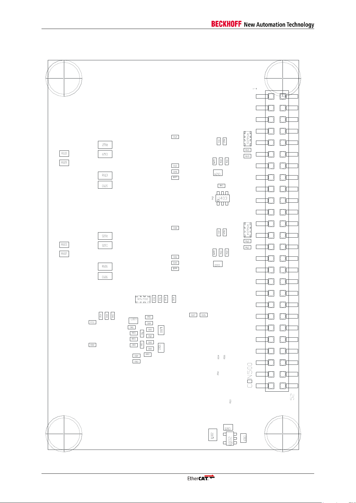
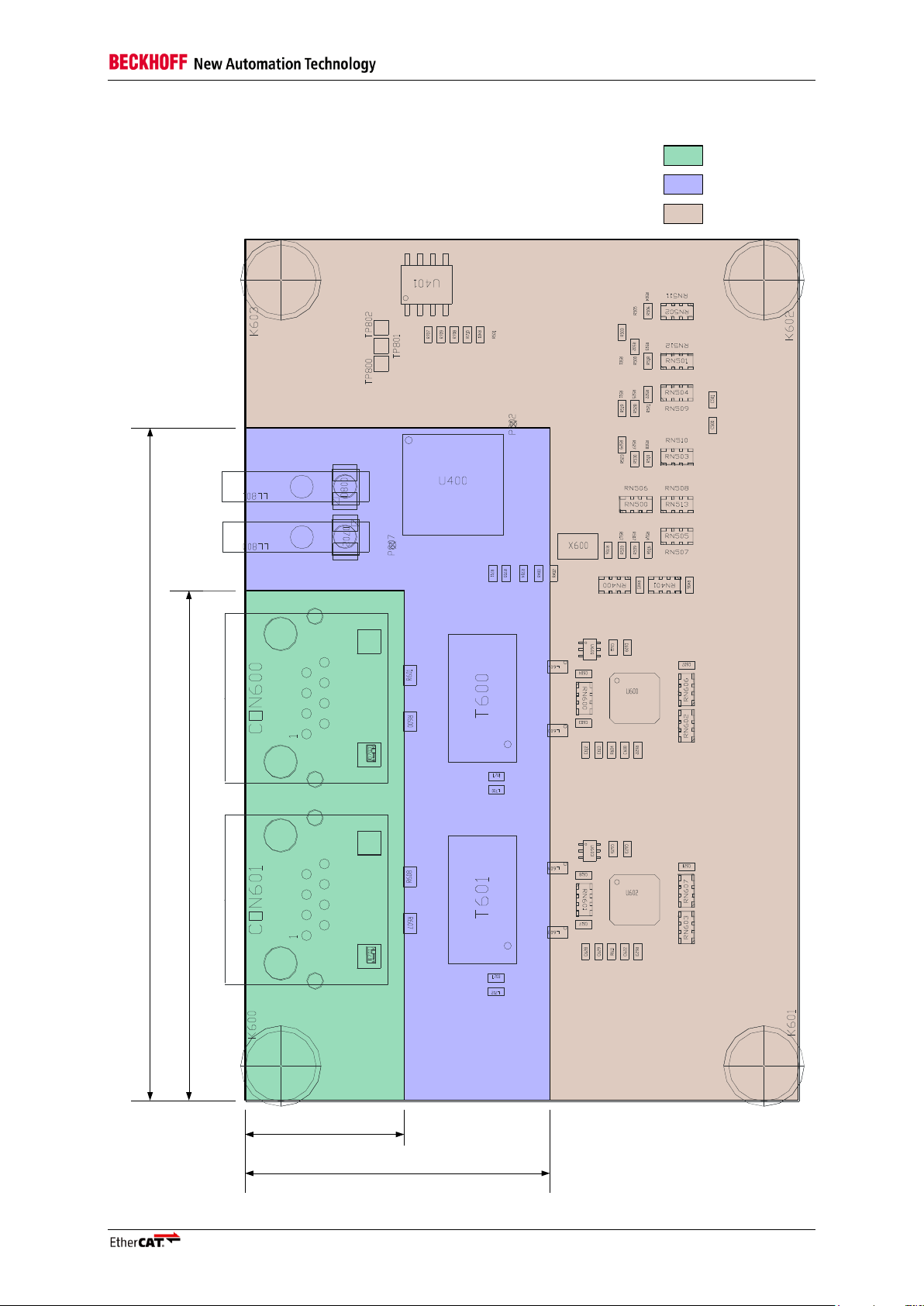
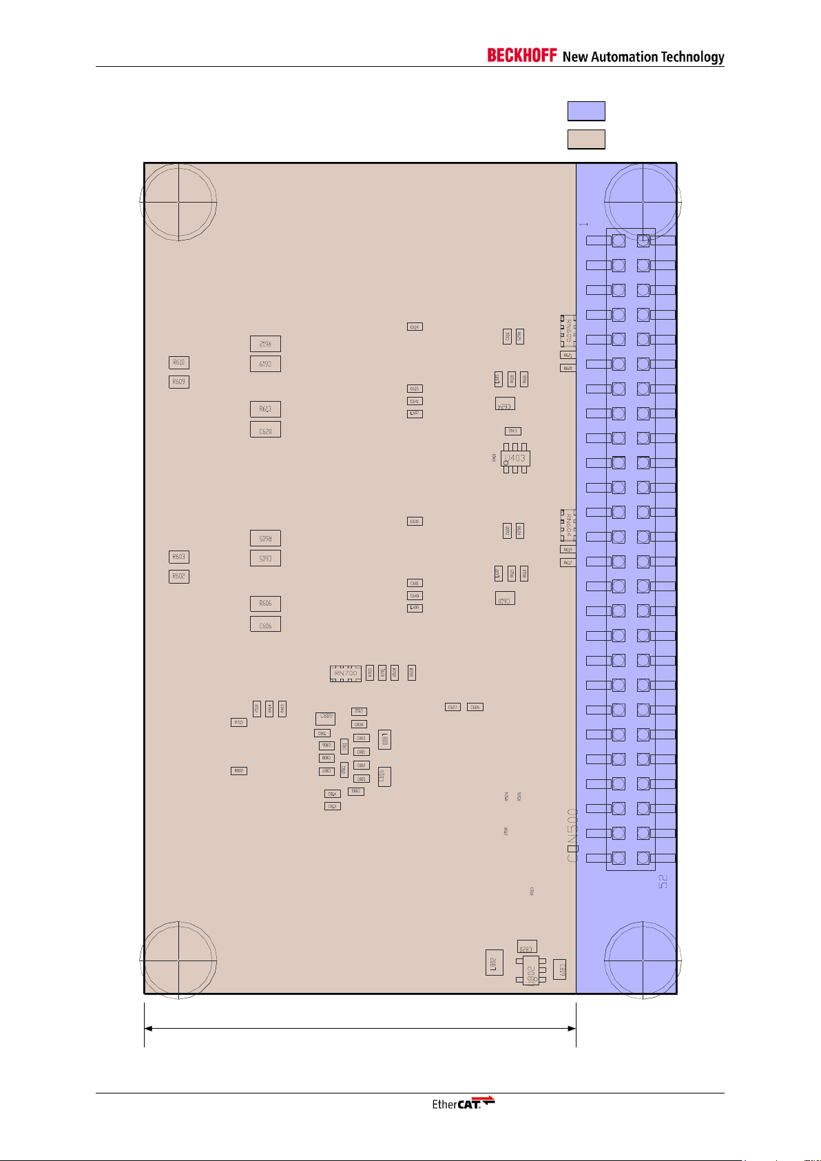
4 Component Placement Specification
In the following chapters the component placement specification in terms of reference designators and
component values are listed for the three variants of the FB1111 EtherCAT piggyback controller
board.
4.1 Placed/Unplaced Components
As the variants of the FB1111 are all based on one printed circuit board, the different PDI configurations are achieved by alternative component placements. Figure 3 is an example for placed and unplaced components. Designators for placed components are surrounded by a rectangle. Components
that are not mounted for a specific variant are also referenced by a designator, but without the surrounding rectangle.
Figure 3: Example for placed/unplaced components
Most of the resistor pairs within the PDI configuration area are sharing one pad with each other. When
modifying the resistor configuration care have to be taken in order to connect the corresponding pads
with each other correctly. An example is shown in Figure 4 for single resistors as for an resistor network.
Figure 4: Pads of resistor networks and single resistors
4.2 Power Test Pads
Table 8: Power Test Pads
10 FB1111 Piggyback Controller Board
Page 17

Component Placement Specification
4.3 FB1111-0142 – 32 bit In/Out digital Interface
4.3.1 Top Side of FB1111-0142
FB1111 Piggyback Controller Board 11
Page 18
Component Placement Specification
4.3.2 Bottom side of FB1111-0142
12 FB1111 Piggyback Controller Board
Page 19

Component Placement Specification
4.4 FB1111-0141 – Serial Peripheral Interface
4.4.1 Top side of FB1111-0141
FB1111 Piggyback Controller Board 13
Page 20

Component Placement Specification
4.4.2 Bottom side of FB1111-0141
14 FB1111 Piggyback Controller Board
Page 21

Component Placement Specification
4.5 FB1111-0140 – 8/16 bit asynchronous Microcontroller Interface
4.5.1 Top side of FB1111-0140
FB1111 Piggyback Controller Board 15
Page 22

Component Placement Specification
4.5.2 Bottom side of FB1111-0140
16 FB1111 Piggyback Controller Board
Page 23

Interfacing with the EL9820 Evaluation Kit
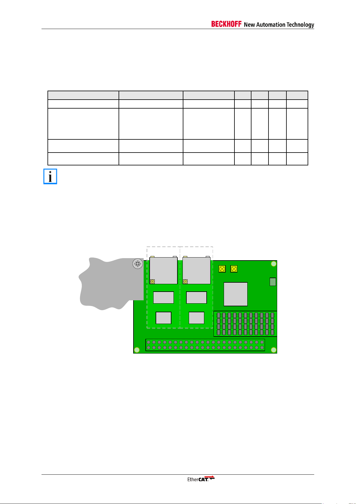
5 Interfacing with the EL9820 Evaluation Kit
As the FB1111 piggyback controller board variant with the sub code 0142 (32 bit In/Out digital Interface) uses all available signals on the PDI connector, it can be programmed to implement the two
remaining PDIs.
Figure 5: EL9803 Adapter board – Top Side
Due to the different PDI connector pinouts in comparison with the variants 0141 and 0140 an additional board is needed, that maps the physical digital PDI signals to the Microcontroller, respectively SPI,
interface of the EL9820 Evaluation Kit. Therefore the EL9803 adapter board can be used to realize all
three available PDIs on the EL9820 Evaluation Kit with just one FB1111-0142.
Figure 5 shows the top side of the EL9803 Adapter Board. The FB1111-0142 has to be placed on the
position, labelled with “FB1111” on the top most right of Figure 5. The adapter board is delivered with
spacer pins at the position, where the FB1111-0142 has to be attached at.
The EL9820 Evaluation Kit connects with the EL9803 Adapter Board from the bottom side (Figure 6)
of the of the adapter board. The holes labelled with “As uC” and “SPI” are referencing the position of
the EL9820 Evaluation Board for the desired Process Data Interface. In addition to the labelled position holes two LEDs are placed on the board (bottom right edge of Figure 5). The left LED indicates
physical SPI mapping between EL9820 and EL9803. The right one indicates asynchronous Microcontroller interfacing.
Only 50 PDI signals are provided by the EL9820 Evaluation Kit in comparison to the 52 signals of the
EtherCAT piggyback controller board FB1111-0142, respectively the EL9803 Adapter Board. The
boards FB1111-0142 and EL9803 are supporting full functionality of the EtherCAT Evaluation Kit
EL9820. The additional pins will be used in future versions of the EL9820.
FB1111 Piggyback Controller Board 17
Page 24

Interfacing with the EL9820 Evaluation Kit
VCC
GND
+3.3V
PDI4
PDI9
PDI8
PDI7
PDI6
Pin name
0141 - SPI
0140 - 16bit as. µC
PDI4
SPI_IRQ
IRQ
PDI6
EEPROM_Loaded
PDI7
n.c.
ADR[15]
PDI8
GPO[0]
ADR[14]
PDI9
GPO[1]
ADR[13]
Figure 6: EL9803 Adapter board – Bottom Side
The PCB colour may vary between green, black and red.
5.1.1 Left side pin header definition
Figure 7: Left side right angle header pinout
Figure 7 shows the pinout of the header on left side of the EL9803’s top. Depending on the selected
process data interface, the definition of the pins PDI4 and PDI6 to PDI9 are differing. The pin names
given here are based on the ET1100 PDI pinout. Thus detailed information about pin description and
electrical specification of these pins can be found in the ET1100 Hardware Data Sheet that can be
downloaded from the company’s website. An overview of the pinout is given in the following table.
18 FB1111 Piggyback Controller Board
Table 9 Pin description of 8 pin right angle header
Page 25

Interfacing with the EL9820 Evaluation Kit
5.2 EL9820 stacking examples
In this chapter the two stacking alternatives of the EL9803 Adapter Board on the EL9820 Evaluation
Kit is shown. Figure 8 represents the asynchronous microcontroller configuration, while Figure 9
demonstrates the SPI configuration of the three boards.
Figure 8: Microcontroller Configuration with EL9803
Figure 9: SPI Configuration with EL9803
FB1111 Piggyback Controller Board 19
Page 26
Electrical Specification
Note
Additional information about the ratings, operation conditions and DC characteristics can be found in the EtherCAT ET1100 hardware data sheet.
IN
TR 0
ET1100
+5VRUN
Port 0
E²P
GND-Earth
Link 1 Link 0
PHY
0
PDI Configuration
Area
PDI Connector
OUT
TR 1
Port 1
PHY
1
Symbol
Parameter
Condition
Min
Typ
Max
Units
VCC
Board Supply Voltage
4.0
5.0
5.5
V
ICC
Board Supply Current
1 Port
2 Ports
1 Port + full PDI
2 Ports + full PDI
100
140
190
300
350
700
mA
Storage
Storage temperature
-65 105
°C
Ambient
Ambient temperature
-40 70
°C
6 Electrical Specification
6.1 Ratings
Table 10: Typical Ratings
6.2 EMC – Electro magnetic compatibility
For proper protection against damage caused by electrostatic discharge, the top left mounting hole of
the EtherCAT piggyback controller board has to be connected to a massive panel or plate that is connected with GND-Earth. The remaining three holes have to be used for mechanical fixation of the piggyback controller board.
Figure 10: Connection to GND-Earth
Suitable screw dimensions are: M3x6 DIN-7985.
20 FB1111 Piggyback Controller Board
Page 27

Mechanical Specification
Note 1
Pin 1
Pin 52
IN
OUT
Note
The ten holes encapsulated by the ellipsoid in Figure 11 don’t have to be taken
into account, when the piggyback controller board is integrated into a third party
customer device. The holes are only mechanical and therefore do not have any
electrical connection.
7 Mechanical Specification
As the EtherCAT piggyback controller board FB1111-014x can be assembled with customer hardware
to complex end user devices, board dimensions and assembly recommendations have to be taken in
account. In 7.1 the board dimensions including mounting and contact hole positions and diameters
from top view are shown. Panel opening recommendations are shown in section 7.2. All dimensions
are drawn in millimeters.
7.1 Board Dimensions
Figure 11: Board dimensions of the FB1111 – Top View
FB1111 Piggyback Controller Board 21
Page 28

Mechanical Specification
14.1
17.4
2.6
RUN+5V
5.0
7.3
2.54
Ø3.00
OUTIN
7.2 Physical Connector Specification
The Board to Board connector (CON500) can be connected as well from the bottom as from the top
side of the FB1111-014X. The bottom side low profile socket is equivalent to the Samtec
(www.samtec.com) product with the manufacturer number CLH-126-F-D-BE-P-TR. Insertion depth
from top side is 4.7 mm, respectively 3.2 mm from bottom side. A suitable pin header for the low profile socket can also be received from Samtec. The TSM series is suitable for the socket. As an example the pin header with the part number TSM-126-02-L-DV can be used to connect the EtherCAT piggyback controller board FB1111-014x.
7.3 Recommended Panel Opening
Figure 12: Recommended Panel Opening
In Figure 12 the dimensions of a typical panel opening is illustrated. The two ports and the LED break
throughs have to be labelled as shown in the figure.
22 FB1111 Piggyback Controller Board
Page 29
Mechanical Specification
13.5 mm
6 mm
3 mm
51
67
16
30
7.4 Top/Bottom Side Component Height Definition
Figure 13: Component height zones for the top side of FB1111-014X
FB1111 Piggyback Controller Board 23
Page 30
Mechanical Specification
4 mm
3 mm
45
Figure 14: Component height zones for the bottom side of FB1111-014X
24 FB1111 Piggyback Controller Board
Page 31
Appendix
8 Appendix
8.1 Support and Service
Beckhoff and their partners around the world offer comprehensive support and service, making available fast and competent assistance with all questions related to Beckhoff products and system solutions.
8.1.1 Beckhoff’s branch offices and representatives
Please contact your Beckhoff branch office or representative for local support and service on Beckhoff
products!
The addresses of Beckhoff's branch offices and representatives round the world can be found on her
internet pages: http://www.beckhoff.com
You will also find further documentation for Beckhoff components there.
8.2 Beckhoff Headquarters
Beckhoff Automation GmbH
Eiserstr. 5
33415 Verl
Germany
phone: + 49 (0) 5246/963-0
fax: + 49 (0) 5246/963-198
e-mail: info@beckhoff.com
web: www.beckhoff.com
Beckhoff Support
Support offers you comprehensive technical assistance, helping you no only with the application of
individual Beckhoff products, but also with other, wide-ranging services:
support
design, programming and commissioning of complex automation systems
and extensive training program for Beckhoff system components
hotline: + 49 (0) 5246/963-157
fax: + 49 (0) 5246/963-9157
e-mail: support@beckhoff.com
Beckhoff Service
The Beckhoff Service Center supports you in all matters of after-sales service:
on-site service
repair service
spare parts service
hotline service
hotline: + 49 (0) 5246/963-460
fax: + 49 (0) 5246/963-479
e-mail: service@beckhoff.com
FB1111 Piggyback Controller Board 25
 Loading...