

Page 1

Hardware Data Sheet
ET1200
Slave Controller
Section I – Technology
(Online at http://www.beckhoff.com)
Section II – Register Description
(Online at http://www.beckhoff.com)
Section III – Hardware Description
Pinout, Interface description, electrical
and mechanical specification, ET1200
features and registers
Version 1.8
Date: 2014-07-07
Page 2

DOCUMENT ORGANIZATION
Trademarks
Beckhoff®, TwinCAT®, EtherCAT®, Safety over EtherCAT®, TwinSAFE® and XFC® are registered trademarks of and licensed by
Beckhoff Automation GmbH. Other designations used in this publication may be trademarks whose use by third parties for their
own purposes could violate the rights of the owners.
Patent Pending
The EtherCAT Technology is covered, including but not limited to the following German patent applications and patents:
DE10304637, DE102004044764, DE102005009224, DE102007017835 with corresponding applications or registrations in
various other countries.
Disclaimer
The documentation has been prepared with care. The products described are, however, constantly under development. For that
reason the documentation is not in every case checked for consistency with performance data, standards or other
characteristics. In the event that it contains technical or editorial errors, we retain the right to make alterations at any time and
without warning. No claims for the modification of products that have already been supplied may be made on the basis of the
data, diagrams and descriptions in this documentation.
Copyright
© Beckhoff Automation GmbH 07/2014.
The reproduction, distribution and utilization of this document as well as the communication of its contents to others without
express authorization are prohibited. Offenders will be held liable for the payment of damages. All rights reserved in the event of
the grant of a patent, utility model or design.
DOCUMENT ORGANIZATION
The Beckhoff EtherCAT Slave Controller (ESC) documentation covers the following Beckhoff ESCs:
ET1200
ET1100
EtherCAT IP Core for Altera® FPGAs
EtherCAT IP Core for Xilinx® FPGAs
ESC20
The documentation is organized in three sections. Section I and section II are common for all Beckhoff
ESCs, Section III is specific for each ESC variant.
The latest documentation is available at the Beckhoff homepage (http://www.beckhoff.com).
Section I – Technology (All ESCs)
Section I deals with the basic EtherCAT technology. Starting with the EtherCAT protocol itself, the
frame processing inside EtherCAT slaves is described. The features and interfaces of the physical
layer with its two alternatives Ethernet and EBUS are explained afterwards. Finally, the details of the
functional units of an ESC like FMMU, SyncManager, Distributed Clocks, Slave Information Interface,
Interrupts, Watchdogs, and so on, are described.
Since Section I is common for all Beckhoff ESCs, it might describe features which are not available in
a specific ESC. Refer to the feature details overview in Section III of a specific ESC to find out which
features are available.
Section II – Register Description (All ESCs)
Section II contains detailed information about all ESC registers. This section is also common for all
Beckhoff ESCs, thus registers, register bits, or features are described which might not be available in
a specific ESC. Refer to the register overview and to the feature details overview in Section III of a
specific ESC to find out which registers and features are available.
Section III – Hardware Description (Specific ESC)
Section III is ESC specific and contains detailed information about the ESC features, implemented
registers, configuration, interfaces, pinout, usage, electrical and mechanical specification, and so on.
Especially the Process Data Interfaces (PDI) supported by the ESC are part of this section.
Additional Documentation
Application notes and utilities like pinout configuration tools for ET1200 can also be found at the
Beckhoff homepage.
III-II Slave Controller – ET1200 Hardware Description
Page 3
DOCUMENT HISTORY
Version
Comment
0.1
Initial release
0.2
Editorial changes
0.3
Register overview, PDI, Electrical and mechanical spec
0.4
Abbreviations, editorial changes
0.5
Removed RJ45 description (will become part of Section I)
EEPROM_LOADED pull-down resistor recommendation added
Frame processing order example corrected
I2C EEPROM interface description added
MII management interface description added
Corrected Process RAM size in Register Overview
Revision/Build information added
Recommendations for unused input pins added (should not be left open)
EEPROM_SIZE description corrected from Kbyte to Kbit, possible EEPROM
sizes range from 16 Kbit to 4 Mbit
RoHS compliance added
Autonegotiation is mandatory for ESCs
Description of power supply options added
Electrical characteristics added
SPI_IRQ delay added
TX Shift timing diagram and description added
Pin overview table corrected
Internal 27 kΩ PU/PD resistors at EBUS-RX pins added
LED polarity depending on configuration pin setting described
Recommendation for voltage stabilization capacitors added
Description of Digital I/O behavior on watchdog expiration enhanced
EBUS ports are open failsafe
Reset example schematic added
Ethernet PHY requirements and PHY connection schematic added
MI_DATA pull-up requirement added
Editorial changes
1.0
RUN, LINKACT/x) and PERR(x) LED activity level corrected: active high if
pulled down, active low if pulled up
TX Shift description: timing figures corrected, minor changes, moved to MII
Interface chapter
Pin/Signal description overview added
PERR(x) LEDs are only for testing/debugging
Electrical characteristics enhanced
DC Characteristics enhanced: added V
Reset Core
, VID, VIC
Digital I/O and SPI timing characteristics revised
DC SYNC/LATCH signal description and timing characteristics added
MII Interface chapter and MII timing characteristics added
EBUS Interface chapter added
PHY requirements, EEPROM Interface description and MII Management
Interface description moved to Section I
Ambient temperature range instead of junction temperature range
Editorial changes
DOCUMENT HISTORY
Slave Controller – ET1200 Hardware Description III-III
Page 4

DOCUMENT HISTORY
Version
Comment
1.1
Clarified I/O voltage with respect to I/O power supply (only 3.3V I/O with
V
CCI/O
=3.3V, and no 5V input tolerance unless V
CCI/O
=5V)
Update to ET1200 stepping 1
Added/revised OSC_IN, CLK25OUT, and MII TX signal timings
Added soldering profile
PHY address configuration changed
Added feature detail overview, removed redundant feature details
PDI and DC SYNC/LATCH signals are not driven until EEPROM is loaded
Editorial changes
1.2
PHY address configuration chapter added, configuration revised
Enhanced link detection for MII available depending on PHY address
configuration
Ethernet Management Interface: read and write times were interchanged
Editorial changes
1.3
Added reset timing figure and power-on value sample time
Direction of Distributed Clocks SYNC/LATCH signals is configurable
Information on CLK25OUT/CPU_CLK clock output during reset added
Description of internal PU/PD resistors at EBUS_RX pins enhanced
Power supply example schematic clarified
Enhanced package information: MSL and plating material
Digital I/O PDI: added SOF/OUTVALID description
SPI PDI: Read busy signaling not recommended
Editorial changes
1.4
OSC_IN/OSC_OUT pin capacitance added, crystal connection note extended
Release Notes added
Input threshold voltage for OSC_IN added
Renamed Err(x) LED to PERR(x)
Digital I/O PDI: OE_CONF functionality in bidirectional mode corrected
Digital I/O PDI: output event description corrected (EOF mode and WD_TRIG
mode)
SPI PDI: access error if SPI_DI not 1 in the last read byte (not SPI_DO)
AC timing: forwarding delay figures added
Editorial changes
1.5
AC timing: forwarding delay figures MII to MII added
Reset timing figure corrected
Maximum soldering profile added
SPI PDI updated
SII EEPROM interface is a point-to-point connection
Editorial changes
1.6
Update to ET1200-0002
Editorial changes
1.7
Enhanced Link Detection must not be activated if EBUS ports are used
Enhanced Link Detection for MII ports requires PHY address offset = 0
Digital Output principle schematic updated
Chip label updated
Editorial changes
1.8
Update to ET1200-0003
Enhanced Link Detection for MII ports supports PHY address offset 0 and 16
Enhanced Link Detection for MII ports can be disabled at any time
Enhanced Link Detection for EBUS ports is always disabled
MII management interface issues additional MCLK cycle after write accesses
Remote link down signalling time configurable 0x0100[22]
Editorial changes
III-IV Slave Controller – ET1200 Hardware Description
Page 5

CONTENTS
CONTENTS
1 Overview 1
1.1 Frame processing order 2
1.2 Scope of this document 3
1.3 Revision/Build History 3
2 Features and Registers 4
2.1 Features 4
2.2 Register Overview 7
3 Pin Description 10
3.1 Overview 10
3.1.1 Pin Overview 10
3.1.2 Signal Overview 11
3.1.3 PDI Signal Overview 12
3.2 Configuration Pins 13
3.2.1 Chip mode 13
3.2.2 CPU_CLK MODE 13
3.2.3 TX Shift 13
3.2.4 CLK25OUT Enable 14
3.2.5 PHY Address Offset 14
3.2.6 SII EEPROM Size 14
3.3 General ET1200 Pins 15
3.4 SII EEPROM Interface Pins 15
3.5 Distributed Clocks SYNC/LATCH Pins, MII Management Data 16
3.6 LED Signals 16
3.7 Physical Ports and PDI Pins 17
3.7.1 MII Interface 18
3.7.2 EBUS Interface 18
3.7.3 PDI Pins 18
3.7.4 Port 0/1 and PDI[17:8] Signals 19
3.7.5 PDI[7:0] Signals 20
3.8 PDI Signal Pinout depending on selected PDI 20
3.8.1 Digital I/O Pin Out 21
3.8.2 SPI Pin Out 21
3.8.3 EBUS/MII bridge port (Logical port 3) 22
3.9 Power Supply 23
4 MII Interface 24
4.1 MII Interface Signals 24
4.2 PHY Address Configuration 25
4.3 TX Shift Compensation 26
4.4 Timing specifications 27
Slave Controller – ET1200 Hardware Description III-V
Page 6

CONTENTS
5 EBUS/LVDS Interface 28
5.1 EBUS Interface Signals 28
6 PDI Description 29
6.1 PDI Deactivated 29
6.2 Digital I/O Interface 30
6.2.1 Interface 30
6.2.2 Configuration 30
6.2.3 Digital Inputs 30
6.2.4 Digital Outputs 31
6.2.5 Bidirectional mode 32
6.2.6 Output Driver 32
6.2.7 SyncManager Watchdog 32
6.2.8 SOF 33
6.2.9 OUTVALID 33
6.2.10 Timing specifications 33
6.3 SPI Slave Interface 35
6.3.1 Interface 35
6.3.2 Configuration 35
6.3.3 SPI access 35
6.3.4 Commands 36
6.3.5 Address modes 36
6.3.6 Interrupt request register (AL Event register) 36
6.3.7 Write access 37
6.3.8 Read access 37
6.3.9 SPI access errors and SPI status flag 37
6.3.10 EEPROM_LOADED 37
6.3.11 Timing specifications 38
7 Distributed Clocks SYNC/LATCH Signals 43
7.1 Signals 43
7.2 Timing specifications 43
8 SII EEPROM Interface (I²C) 44
8.1 Signals 44
8.2 Timing specifications 44
9 Example Schematics 45
9.1 Clock Adoption 45
9.2 Power supply 46
9.3 Dual purpose configuration input/LED output pins 47
9.4 PHY Connection 47
9.5 LVDS termination 48
9.6 RBIAS resistor 48
9.7 Reset Logic 48
III-VI Slave Controller – ET1200 Hardware Description
Page 7

CONTENTS
10 Electrical Specifications and Timings 49
10.1 Absolute Maximum Ratings 49
10.2 Electrical Characteristics 49
11 Mechanical Specifications 55
11.1 Package Information 55
11.2 Moisture Sensitivity and Storage 57
11.3 Soldering Profile 58
11.4 Ordering codes 59
12 Appendix 60
12.1 Support and Service 60
12.1.1 Beckhoff’s branch offices and representatives 60
12.2 Beckhoff Headquarters 60
Slave Controller – ET1200 Hardware Description III-VII
Page 8

TABLES
TABLES
Table 1: ET1200 Main Features .............................................................................................................. 1
Table 2: Frame Processing Order ........................................................................................................... 2
Table 3: Revision/Build History................................................................................................................ 3
Table 4: ET1200 Feature Details ............................................................................................................ 4
Table 5: Legend ....................................................................................................................................... 6
Table 6: Legend ....................................................................................................................................... 7
Table 7: Register Overview ..................................................................................................................... 7
Table 8: Pin Overview ........................................................................................................................... 10
Table 9: Signal Overview ....................................................................................................................... 11
Table 10: PDI signal overview ............................................................................................................... 12
Table 11: Chip Mode ............................................................................................................................. 13
Table 12: CPU_CLK Mode .................................................................................................................... 13
Table 13: TX Shift .................................................................................................................................. 13
Table 14: CLK_25OUT Enable .............................................................................................................. 14
Table 15: PHY Address Offset .............................................................................................................. 14
Table 16: SII EEPROM Size .................................................................................................................. 14
Table 17: General pins .......................................................................................................................... 15
Table 18: SII EEPROM pins .................................................................................................................. 15
Table 19: DC SYNC/LATCH and MII Management pins ....................................................................... 16
Table 20: LED pins ................................................................................................................................ 16
Table 21: Combinations of Chip modes and PDIs ................................................................................ 17
Table 22: Port 0/1 and PDI signals (Configuration and chip mode 00) ................................................. 19
Table 23: Port 0/1 and PDI signals (chip modes 10/11) ........................................................................ 19
Table 24: PDI pins ................................................................................................................................. 20
Table 25: Mapping of Digital I/O Interface ............................................................................................. 21
Table 26: Mapping of SPI Interface ....................................................................................................... 21
Table 27: Mapping of EBUS Bridge signals .......................................................................................... 22
Table 28: Mapping of MII Bridge signals ............................................................................................... 22
Table 29: Power supply options (all voltages nomal) ............................................................................ 23
Table 30: Power supply ......................................................................................................................... 23
Table 31: MII Interface signals .............................................................................................................. 25
Table 32: TX Shift Timing characteristics .............................................................................................. 26
Table 33: MII timing characteristics ....................................................................................................... 27
Table 34: EBUS Interface signals ......................................................................................................... 28
Table 35: Available PDIs for ET1200 .................................................................................................... 29
Table 36: ET1200 Digital I/O signals ..................................................................................................... 30
Table 37: Digital I/O timing characteristics ET1200 .............................................................................. 33
Table 38: SPI signals ............................................................................................................................. 35
Table 39: SPI commands CMD0 and CMD1 ......................................................................................... 36
Table 40: Address modes ...................................................................................................................... 36
Table 41: Interrupt request register transmission .................................................................................. 36
Table 42: SPI timing characteristics ET1200 ........................................................................................ 38
Table 43: Read/Write timing diagram symbols ...................................................................................... 39
Table 44: Distributed Clocks signals ..................................................................................................... 43
Table 45: DC SYNC/LATCH timing characteristics ET1200 ................................................................. 43
Table 46: I²C EEPROM signals ............................................................................................................. 44
Table 47: EEPROM timing characteristics ............................................................................................ 44
Table 48: Absolute Maximum Ratings ................................................................................................... 49
Table 49: Operating Conditions ............................................................................................................. 49
Table 50: DC Characteristics ................................................................................................................. 50
Table 51: DC Characteristics (Supply current) ...................................................................................... 51
Table 52: AC Characteristics ................................................................................................................. 52
Table 53: Forwarding Delays ................................................................................................................. 54
Table 54: Absolute Maximum Storage Conditions ................................................................................ 57
Table 55: Example Soldering Profile ..................................................................................................... 59
III-VIII Slave Controller – ET1200 Hardware Description
Page 9

FIGURES
FIGURES
Figure 1: ET1200 Block Diagram ............................................................................................................ 1
Figure 2: Frame Processing .................................................................................................................... 2
Figure 3: MII Interface signals ............................................................................................................... 24
Figure 4: TX Shift Timing Diagram ........................................................................................................ 26
Figure 5: MII timing RX signals.............................................................................................................. 27
Figure 6: EBUS Interface Signals .......................................................................................................... 28
Figure 7: ET1200 Digital I/O Signals ..................................................................................................... 30
Figure 8: Digital Output Principle Schematic ......................................................................................... 31
Figure 9: Bidirectional mode: Input/Output connection (R=4.7 kΩ recommended) .............................. 32
Figure 10: Digital Input: Input data sampled at SOF, I/O can be read in the same frame .................... 34
Figure 11: Digital Input: Input data sampled with LATCH_IN ................................................................ 34
Figure 12: Digital Output timing ............................................................................................................. 34
Figure 13: Bidirectional Mode timing ..................................................................................................... 34
Figure 14: SPI master and slave interconnection.................................................................................. 35
Figure 15: Basic SPI_DI/SPI_DO timing (*refer to timing diagram for relevant edges of SPI_CLK) .... 39
Figure 16: SPI read access (2 byte addressing, 2 byte read data) with BUSY and separate status
reading ................................................................................................................................................... 40
Figure 17: SPI write access (2 byte addressing, 1 byte write data) ...................................................... 41
Figure 18: SPI write access (3 byte addressing, 1 byte write data) ...................................................... 42
Figure 19: Distributed Clocks signals .................................................................................................... 43
Figure 20: LatchSignal timing ................................................................................................................ 43
Figure 21: SyncSignal timing ................................................................................................................. 43
Figure 22: I²C EEPROM signals ............................................................................................................ 44
Figure 23: Quartz crystal connection ..................................................................................................... 45
Figure 24: Quartz crystal Clock source for ET1200 and Ethernet PHYs .............................................. 45
Figure 25: Oscillator clock source for ET1200 and Ethernet PHYs ...................................................... 46
Figure 26: ET1200 power supply........................................................................................................... 46
Figure 27: Dual purpose configuration input/LED output pins ............................................................... 47
Figure 28: PHY Connection ................................................................................................................... 47
Figure 29: LVDS termination ................................................................................................................. 48
Figure 30: RBIAS resistor ...................................................................................................................... 48
Figure 31: Reset Logic .......................................................................................................................... 48
Figure 32: Reset Timing ........................................................................................................................ 53
Figure 33: Package Outline ................................................................................................................... 55
Figure 34: Dimensions ........................................................................................................................... 56
Figure 35: Notes .................................................................................................................................... 56
Figure 36: Chip Label ............................................................................................................................ 56
Figure 37: Maximum Soldering Profile .................................................................................................. 58
Figure 38: Example Soldering Profiles .................................................................................................. 58
Slave Controller – ET1200 Hardware Description III-IX
Page 10

ABBREVIATIONS
(x)
Logical Port x
[z]
Bit z
{y}
Physical Port y
µC
Microcontroller
ADR
Address
AL
Application Layer
BD
Bidirectional
BHE
Bus High Enable
CMD
Command
DC
Distributed Clock
Dir.
Pin direction
DL
Data Link Layer
ECAT
EtherCAT
EMC
Electromagnetic Compatibility
EMI
Electromagnetic Interference
EOF
End of Frame
EP
Exposed Pad
ESC
EtherCAT Slave Controller
ESI
EtherCAT Slave Information
FMMU
Fieldbus Memory Management Unit
GPI
General Purpose Input
GPO
General Purpose Output
I
Input
I/O
Input or Output
IRQ
Interrupt Request
LDO
Low Drop-Out regulator
LI-
LVDS RX-
LI+
LVDS RX+
LO-
LVDS TX-
LO+
LVDS TX+
MAC
Media Access Controller
MDIO
Management Data Input / Output
MI
(PHY) Management Interface
MII
Media Independent Interface
MISO
Master In – Slave Out
MOSI
Master Out – Slave In
n.a.
not available
n.c.
not connected
O
Output
PD
Pull-down
PDI
Process Data Interface
PLL
Phase Locked Loop
PU
Pull-up
QFN
Quad Flat package No leads
SII
Slave Information Interface
SM
SyncManager
SOF
Start of Frame
SPI
Serial Peripheral Interface
UI
Unused Input (PDI: PD, others: GND)
WD
Watchdog
WPD
Weak Pull-down, sufficient only for configuration signals
WPU
Weak Pull-up, sufficient only for configuration signals
ABBREVIATIONS
III-X Slave Controller – ET1200 Hardware Description
Page 11
Overview
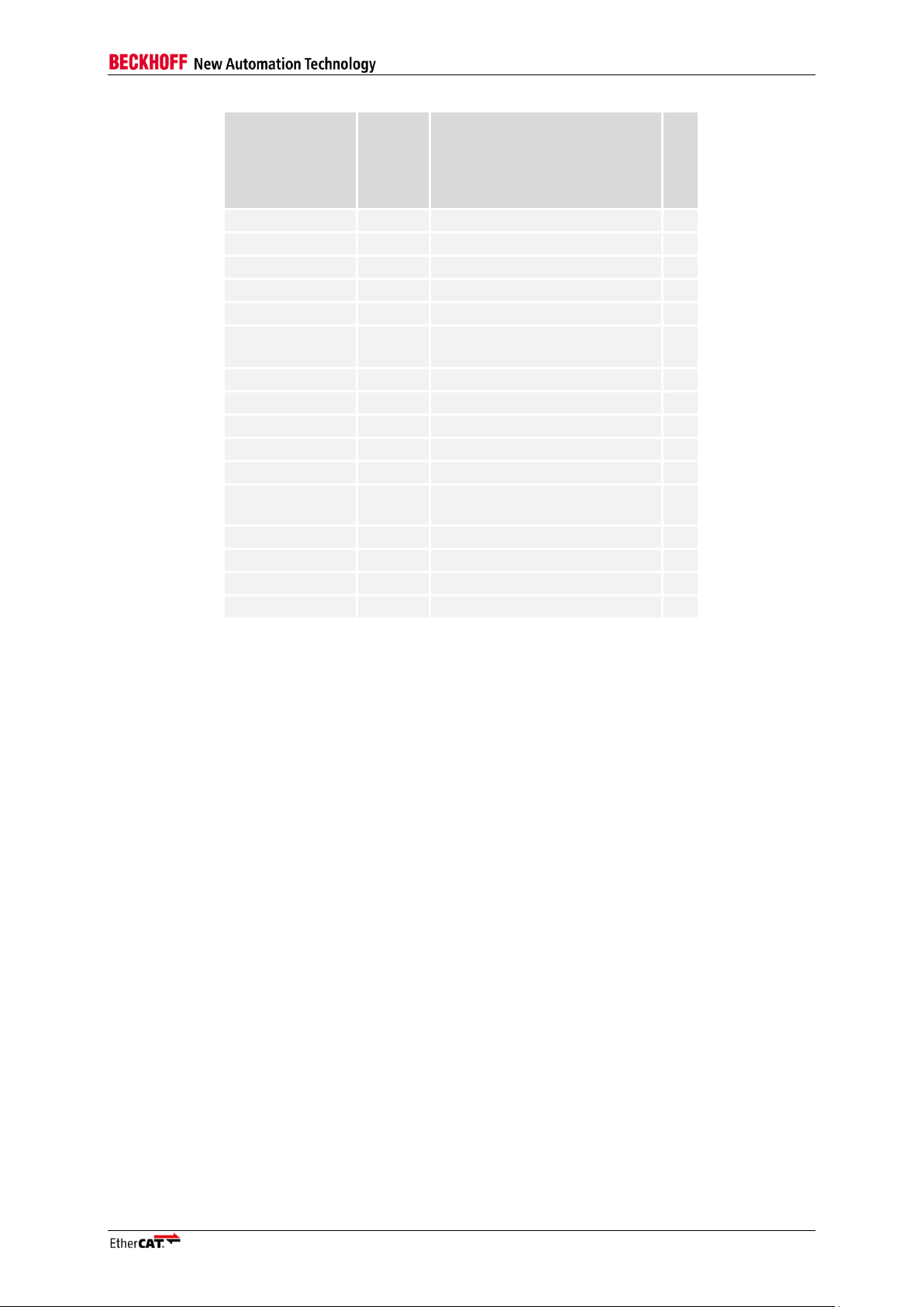
Feature
ET1200
Ports
2 permanent ports, optional one additional bridge port (each EBUS or
MII, max. one MII port)
FMMUs
3
SyncManagers
4
RAM
1 Kbyte
Distributed Clocks
Yes, 64 bit
Process Data Interfaces
16 Bit Digital I/O (unidirectional/bidirectional)
SPI Slave
Power supply
Two integrated voltage regulators (LDO) for I/O (5V to 3.3V) and logic
core/PLL (5V/3.3V to 2.5V), optional external power supply for I/O and
logic core/PLL.
I/O
3.3V compatible I/O
Package
QFN48 (7x7 mm2)
Other features
Internal 1GHz PLL
Clock output for external devices (10, 20, 25 MHz)
ECAT
Processing
Unit
AutoForwarder +
Loopback
SyncManager
FMMU
ESC address space
User RAMRegisters Process RAM
EEPROM
Distributed
Clocks
Monitoring Status
Reset
PHY
Management
Reset
SYNC LEDsI²C EEPROM
PHY MI
SPI / Digital I/O0 1 3
EBUS/MII ports
LATCH
PDI
ECAT Interface PDI Interface
1 Overview
The ET1200 ASIC is an EtherCAT Slave Controller (ESC). It takes care of the EtherCAT
communication as an interface between the EtherCAT fieldbus and the slave application. The ET1200
supports different applications, from simple digital I/O nodes without external logic up to designs with a
µController and Distributed Clocks.
Table 1: ET1200 Main Features
The general functionality of the ET1200 EtherCAT Slave Controller (ESC) is shown in Figure 1:
Slave Controller – ET1200 Hardware Description III-1
Figure 1: ET1200 Block Diagram
Page 12
Overview
Number of Ports
Frame processing order
2
0→EtherCAT Processing Unit→1 / 1→0
3
0→EtherCAT Processing Unit→3 / 3→1 / 1→0
1
Port 1
Auto-
Forwarder
1
Port 3
Auto-
Forwarder
Port 0
Auto-
Forwarder
Loopback function
EtherCAT
Processing Unit
Loopback function
Loopback function
ET1200
port 1 closed
port 1 open
port 3 open
port 3 closed
port 0 open
or all ports
closed
port 0 closed
1.1 Frame processing order
The ET1200 supports two ports (logical ports 0 and 1) or three ports (logical ports 0, 1, and 3). The
frame processing order of the ET1200 depends on the number of ports (logical port numbers are
used):
Table 2: Frame Processing Order
Figure 2 shows the frame processing in general:
Figure 2: Frame Processing
III-2 Slave Controller – ET1200 Hardware Description
Page 13

Overview
Revision
Register 0x0001
Build
Register 0x0002:0x0003
Stepping
0x00
0x0000
ET1200-0000 or
ET1200-0001
0x00
0x0002
ET1200-0002
0x00
0x0003
ET1200-0003
1.2 Scope of this document
This documentation refers to stepping ET1200-0003.
1.3 Revision/Build History
Table 3: Revision/Build History
The stepping code is printed on the devices, do not confuse the stepping code with the ordering
codes.
Slave Controller – ET1200 Hardware Description III-3
Page 14
Features and Registers
Feature
ET1200
-0003
EtherCAT Ports
2-3
Permanent ports
2
Optional Bridge port 3 (EBUS or MII)
c
EBUS ports
1-3
MII ports
0-1
RMII ports
-
RGMII ports
-
Port 0
-
Ports 0, 1
x
Ports 0, 1, 2
-
Ports 0, 1, 3
x
Ports 0, 1, 2, 3
-
Slave Category
Full Slave
Position addressing
x
Node addressing
x
Logical addressing
x
Broadcast addressing
x
Physical Layer General Features
FIFO Size configurable (0x0100[18:16])
x
FIFO Size default from SII EEPROM
-
Auto-Forwarder checks CRC and SOF
x
Forwarded RX Error indication, detection
and Counter (0x0308:0x030B)
x
Lost Link Counter (0x0310:0x0313)
x
Prevention of circulating frames
x
Fallback: Port 0 opens if all ports are
closed
x
VLAN Tag and IP/UDP support
x
Enhanced Link Detection per port
configurable
-
EBUS Features
Low Jitter
x
Enhanced Link Detection supported
-
Enhanced Link Detection compatible
X
EBUS signal validation
X
LVDS Transceiver internal
X
LVDS sample rate [MHz]
1,000
Remote link down signaling time
configurable 0x0100[22]
x
General Ethernet Features (MII/RMII/RGMII)
MII Management Interface
(0x0510:0x051F)
x
Supported PHY Address Offsets
0/16
Individual port PHY addresses
-
Port PHY addresses readable
-
Link Polarity configurable
-
Enhanced Link Detection supported
x
FX PHY support (native)
-
PHY reset out signals
-
Link detection using PHY signal (LED)
x
MI link status and configuration
-
MI controllable by PDI (0x0516:0x0517)
-
MI read error (0x0510.13)
-
MI PHY configuration update status
(0x0518.5)
-
MI preamble suppression
-
Additional MCLK
x
Gigabit PHY configuration
-
Gigabit PHY register 9 relaxed check
-
FX PHY configuration
-
Transparent Mode
-
Feature
ET1200
-0003
MII Features
CLK25OUT as PHY clock source
x
Bootstrap TX Shift settings
x
Automatic TX Shift setting (with TX_CLK)
-
TX Shift not necessary (PHY TX_CLK as
clock source)
-
FIFO size reduction steps
1
PDI General Features
Increased PDI performance
-
Extended PDI Configuration
(0x0152:0x0153)
x
PDI Error Counter (0x030D)
-
PDI Error Code (0x030E)
-
CPU_CLK output (10, 20, 25 MHz)
x
SOF, EOF, WD_TRIG and WD_STATE
independent of PDI
-
Available PDIs and PDI features
depending on port configuration
x
PDI selection at run-time (SII EEPROM)
x
PDI active immediately (SII EEPROM
settings ignored)
-
PDI function acknowledge by write
-
PDI Information register 0x014E:0x014F
-
Digital I/O PDI
x
Digital I/O width [bits]
8/16
PDI Control register value
(0x0140:0x0141)
4
Control/Status signals:
2/0
1,2
LATCH_IN
x2
SOF
x2
OUTVALID
x2
WD_TRIG
x2
OE_CONF
-
OE_EXT
-
EEPROM_
Loaded
-
WD_STATE
-
EOF
-
Granularity of direction configuration [bits]
2
Bidirectional mode
x
Output high-Z if WD expired
x
Output 0 if WD expired
-
Output with EOF
x
Output with DC SyncSignals
x
Input with SOF
x
Input with DC SyncSignals
x
1
2
2 Features and Registers
2.1 Features
Table 4: ET1200 Feature Details
III-4 Slave Controller – ET1200 Hardware Description
Shared control/status signals: LATCH_IN/SOF and
OUT_VALID/WD_TRIGGER
Availability depending on port configuration
Page 15
Features and Registers
Feature
ET1200
-0003
SPI Slave PDI
x
Max. SPI clock [MHz]
6-20 (SPI
mode dep.)
SPI modes configurable (0x0150[1:0])
x
SPI_IRQ driver configurable (0x0150[3:2])
x
SPI_SEL polarity configurable (0x0150.4)
x
Data out sample mode configurable
(0x0150.5)
x
Busy signaling
x
Wait State byte(s)
-
Number of address extension byte(s)
1
2/4 Byte SPI master support
-
Extended error detection (read busy
violation)
-
SPI_IRQ delay
x
Status indication
x
EEPROM_
Loaded signal
x
Asynchronous µController PDI
-
Synchronous µController PDI
-
EtherCAT Bridge (port 3, EBUS/MII)
x
General Purpose I/O
x
GPO bits
0-12
GPI bits
-
GPIO available independent of PDI or port
configuration
-
GPIO available without PDI
-
Concurrent access to GPO by ECAT and
PDI
x
ESC Information
Basic Information (0x0000:0x0006)
x
Port Descriptor (0x0007)
x
ESC Features supported (0x0008:0x0009)
x
Extended ESC Feature Availability in User
RAM (0x0F80 ff.)
-
Write Protection (0x0020:0x0031)
x
Data Link Layer Features
ECAT Reset (0x0040)
x
PDI Reset (0x0041)
-
ESC DL Control (0x0100:0x0103) bytes
4
EtherCAT only mode (0x0100.0)
x
Temporary loop control (0x0100.1)
x
FIFO Size configurable (0x0100[18:16])
x
Configured Station Address
(0x0010:0x0011)
x
Configured Station Alias (0x0100.24,
0x0012:0x0013)
x
Physical Read/Write Offset
(0x0108:0x0109)
x
Application Layer Features
Extended AL Control/Status bits
(0x0120[15:5], 0x0130[15:5])
x
AL Status Emulation (0x0140.8)
x
AL Status Code (0x0134:0x0135)
x
Interrupts
ECAT Event Mask (0x0200:0x0201)
x
AL Event Mask (0x0204:0x0207)
x
ECAT Event Request (0x0210:0x0211)
x
AL Event Request (0x0220:0x0223)
x
SyncManager activation changed
(0x0220.4)
x
SyncManager watchdog expiration
(0x0220.6)
-
Error Counters
RX Error Counter (0x0300:0x0307)
x
Forwarded RX Error Counter
(0x0308:0x030B)
x
ECAT Processing Unit Error Counter
(0x030C)
-
PDI Error Counter (0x030D)
-
Lost Link Counter (0x0310:0x0313)
x
Feature
ET1200
-0003
Watchdog
Watchdog Divider configurable
(0x0400:0x0401)
x
Watchdog Process Data
x
Watchdog PDI
x
Watchdog Counter Process Data (0x0442)
x
Watchdog Counter PDI (0x0443)
x
SII EEPROM Interface (0x0500:0x050F)
EEPROM sizes supported
1 Kbyte-
4 Mbyte
EEPROM size reflected in 0x0502.7
x
EEPROM controllable by PDI
x
EEPROM Emulation by PDI
-
Read data bytes (0x0502.6)
8
Internal Pull-Ups for EEPROM_CLK and
EEPROM_DATA
x
FMMUs
3
Bit-oriented operation
x
SyncManagers
4
Watchdog trigger generation for 1 Byte
Mailbox configuration independent of
reading access
x
SyncManager Event Times (+0x8[7:6])
-
Buffer state (+0x5[7:6])
-
Distributed Clocks
x
Width
64
Sync/Latch signals
1-23
SyncManager Event Times
(0x09F0:0x09FF)
-
DC Receive Times
x
DC Time Loop Control controllable by PDI
-
DC activation by EEPROM
(0x0140[11:10])
-
Propagation delay measurement with
traffic (BWR/FPWR 0x900 detected at
each port)
-
LatchSignal state in Latch Status register
(0x09AE:0x09AF)
-
SyncSignal Auto-Activation (0x0981.3)
-
SyncSignal 32 or 64 bit Start Time
(0x0981.4)
-
SyncSignal Late Activation (0x0981[6:5])
-
SyncSignal debug pulse (0x0981.7)
-
SyncSignal Activation State 0x0984)
-
Reset filters after writing filter depth
-
ESC Specific Registers (0x0E00:0x0EFF)
Product and Vendor ID
-
POR Values
x
FPGA Update (online)
-
Process RAM and User RAM
Process RAM (0x1000 ff.) [Kbyte]
1
User RAM (0x0F80:0x0FFF)
x
Extended ESC Feature Availability in User
RAM
-
Additional EEPROMs
1
SII EEPROM (I²C)
x
FPGA configuration EEPROM
-
LED Signals
RUN LED
x
RUN LED override
-
Link/Activity(x) LED per port
x
PERR(x) LED per port
x
Device ERR LED
-
STATE_RUN LED
-
3
Slave Controller – ET1200 Hardware Description III-5
SYNC/LATCH[1] available if no MII port is used.
Page 16
Features and Registers
Feature
ET1200
-0003
Optional LED states
RUN LED: Bootstrap
x
RUN LED: Booting
-
RUN LED: Device identification
-
RUN LED: loading SII EEPROM
-
Error LED: SII EEPROM loading error
-
Error LED: Invalid hardware configuration
-
Error LED: Process data watchdog timeout
-
Error LED: PDI watchdog timeout
-
Link/Activity: port closed
-
Link/Activity: local auto-negotiation error
-
Link/Activity: remote auto-negotiation error
-
Link/Activity: unknown PHY auto-
negotiation error
-
LED test
-
Clock supply
Crystal
x
Crystal oscillator
x
TX_CLK from PHY
x
25ppm clock source accuracy
x
Internal PLL
x
Feature
ET1200
-0003
Power Supply Voltages
1-3
I/O Voltage
3.3 V
x
3.3V / 5V tolerant
-
5 V
(x)
Core Voltage
2.5V
Internal LDOs
2
LDO supply voltage
3.3V/5V
Core Voltage
x
I/O Voltage
x
Package
QFN48
Size [mm²]
7x7
Original Release date
11/2006
Configuration and Pinout calculator (XLS)
x
Register Configuration
fixed
Symbol
Description
x
available
-
not available
c
configurable
Table 5: Legend
III-6 Slave Controller – ET1200 Hardware Description
Page 17
Features and Registers
Symbol
Description
x
Available
-
Not available
Address
Length
(Byte)
Description
ET1200
0x0000
1
Type x 0x0001
1
Revision
x
0x0002:0x0003
2
Build x 0x0004
1
FMMUs supported
x
0x0005
1
SyncManagers supported
x
0x0006
1
RAM Size
x
0x0007
1
Port Descriptor
x
0x0008:0x0009
2
ESC Features supported
x
0x0010:0x0011
2
Configured Station Address
x
0x0012:0x0013
2
Configured Station Alias
x
0x0020
1
Write Register Enable
x
0x0021
1
Write Register Protection
x
0x0030
1
ESC Write Enable
x
0x0031
1
ESC Write Protection
x
0x0040
1
ESC Reset ECAT
x
0x0041
1
ESC Reset PDI
-
0x0100:0x0101
2
ESC DL Control
x
0x0102:0x0103
2
Extended ESC DL Control
x
0x0108:0x0109
2
Physical Read/Write Offset
x
0x0110:0x0111
2
ESC DL Status
x
0x0120
5 bits
[4:0]
AL Control
x
0x0120:0x0121
2
AL Control
x
0x0130
5 bits
[4:0]
AL Status
x
0x0130:0x0131
2
AL Status
x
0x0134:0x0135
2
AL Status Code
x
0x0138
1
RUN LED Override
-
0x0139
1
ERR LED Override
-
0x0140
1
PDI Control
x
2.2 Register Overview
An EtherCAT Slave Controller (ESC) has an address space of 64 Kbyte. The first block of 4 Kbyte
(0x0000:0x0FFF) is dedicated for registers. The process data RAM starts at address 0x1000, its size
is 1 Kbyte (end address 0x13FF).
Table 7 gives an overview of the available registers.
Table 6: Legend
Table 7: Register Overview
Slave Controller – ET1200 Hardware Description III-7
Page 18
Features and Registers
Address
Length
(Byte)
Description
ET1200
0x0141
1
ESC Configuration
x
0x014E:0x014F
2
PDI Information
-
0x0150
1
PDI Configuration
x
0x0151
1
DC Sync/Latch Configuration
x
0x0152:0x0153
2
Extended PDI Configuration
x
0x0200:0x0201
2
ECAT Event Mask
x
0x0204:0x0207
4
PDI AL Event Mask
x
0x0210:0x0211
2
ECAT Event Request
x
0x0220:0x0223
4
AL Event Request
x
0x0300:0x0307
4x2
Rx Error Counter[3:0]
x
0x0308:0x030B
4x1
Forwarded Rx Error
counter[3:0]
x
0x030C
1
ECAT Processing Unit Error
Counter
0x030D
1
PDI Error Counter
-
0x030E
1
PDI Error Code
-
0x0310:0x0313
4x1
Lost Link Counter[3:0]
x
0x0400:0x0401
2
Watchdog Divider
x
0x0410:0x0411
2
Watchdog Time PDI
x
0x0420:0x0421
2
Watchdog Time Process Data
x
0x0440:0x0441
2
Watchdog Status Process Data
x
0x0442
1
Watchdog Counter Process
Data
x
0x0443
1
Watchdog Counter PDI
x
0x0500:0x050F
16
SII EEPROM Interface
x
0x0510:0x0515
6
MII Management Interface
x
0x0516:0x0517
2
MII Management Access State
-
0x0518:0x051B
4
PHY Port Status[3:0]
-
0x0600:0x06FC
16x13
FMMU[15:0]
3
0x0800:0x087F
16x8
SyncManager[15:0]
4
0x0900:0x090F
4x4
DC – Receive Times[3:0]
x
0x0918:0x091F
8
DC – Receive Time EPU
x
0x0920:0x0935
24
DC – Time Loop Control Unit
x
0x0910:0x0917
8
DC – System Time
x
0x0936
1
DC – Receive Time Latch
mode
x
0x0980
1
DC – Cyclic Unit Control
x
0x0981
1
DC – Activation
x
0x0982:0x0983
2
DC – Pulse length of
SyncSignals
x
0x0984
1
DC – Activation Status
-
0x098E:0x09A7
26
DC – SYNC Out Unit
x
0x09A8
1
DC – Latch0 Control
x
0x09A9
1
DC – Latch1 Control
x
III-8 Slave Controller – ET1200 Hardware Description
Page 19
Features and Registers
Address
Length
(Byte)
Description
ET1200
0x09AE
1
DC – Latch0 Status
x
0x09B0:0x09B7
8
DC – Latch0 Positive Edge
x
0x09B8:0x09BF
8
DC – Latch0 Negative Edge
x
0x09C0:0x09C7
8
DC – Latch1 Positive Edge
x
0x09C7:0x09CF
8
DC – Latch1 Negative Edge
x
0x09F0:0x09F3
0x09F8:0x09FF
12
DC – SyncManager Event
Times
-
0x0E00:0x0E03
4
Power-On Values (Bits)
8
0x0E00:0x0E07
8
Product ID
-
0x0E08:0x0E0F
8
Vendor ID
-
0x0E10
1
ESC Health Status
-
0x0F00:0x0F03
4
Digital I/O Output Data
x
0x0F10:0x0F17
8
General Purpose Outputs
[Byte]
2
0x0F18:0x0F1F
8
General Purpose Inputs [Byte]
-
0x0F80:0x0FFF
128
User RAM
x
0x1000:0x1003
4
Digital I/O Input Data
io
0x1000 ff.
Process Data RAM [Kbyte]
1
Slave Controller – ET1200 Hardware Description III-9
Page 20
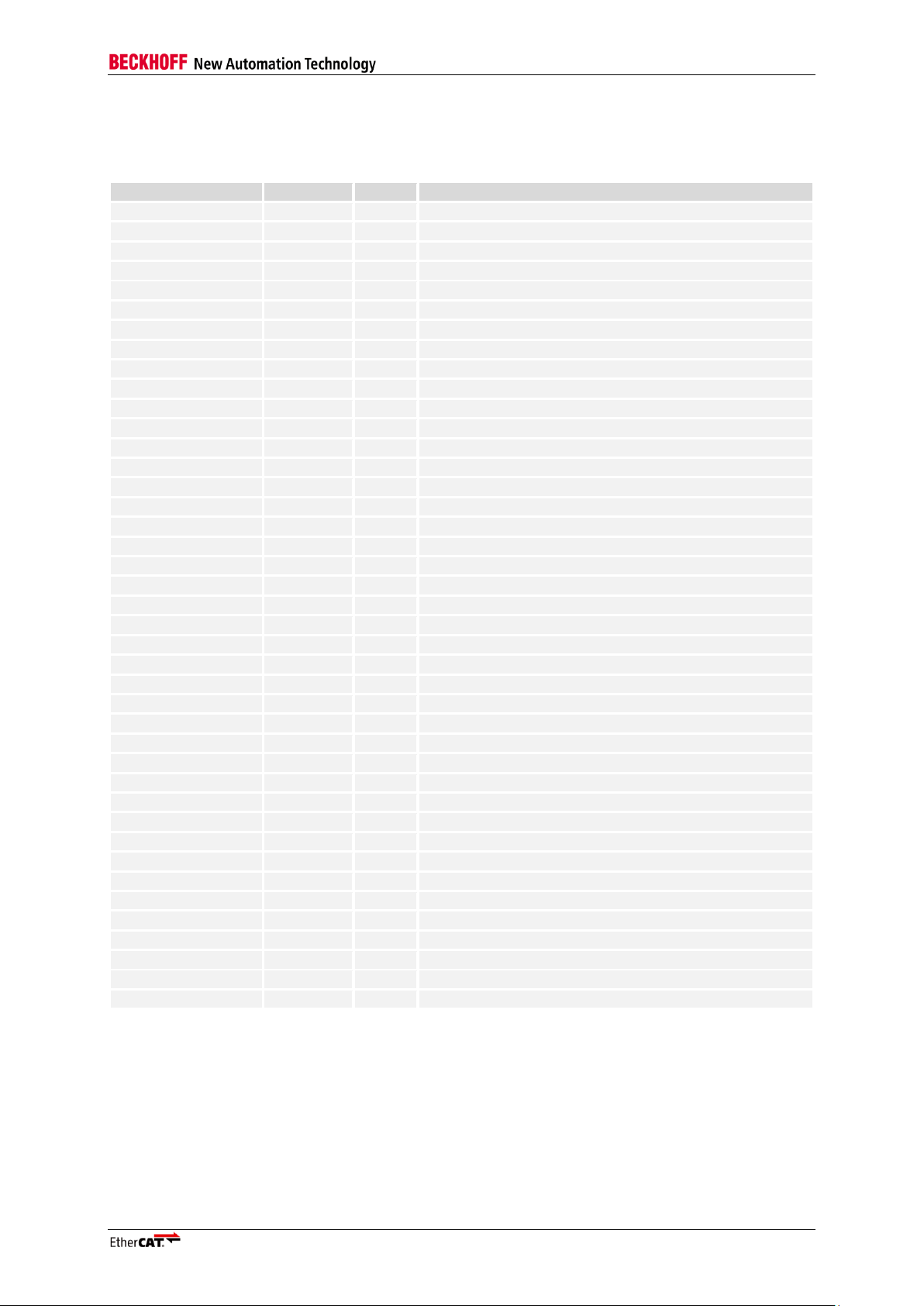
Pin Description
Pin
Pin name
Dir.
Int.
PU/PD
Pin
Pin name
Dir.
Int.
PU/PD
EP
GND 25
RBIAS
1
TESTMODE
I
WPD
26
Reset
BD
WPU
2
EBUS{1}-RX-/LINK_MII
LI-/I
27 kΩ PU
27
PDI[17]/RX_D[3]
BD 3
EBUS{1}-RX+/RX_ERR
LI+/I
27 kΩ PD
28
PDI[16]/RX_D[2]
BD
4
EBUS{0}-TX-
LO-
29
PDI[15]/RX_D[1]
BD
5
EBUS{0}-TX+
LO+
30
PDI[14]/RX_D[0]
BD 6
V
CC I/O
I/O
31
PDI[13]/RX_DV
BD 7
GND
I/O
I/O*
32
PDI[12]/RX_CLK
BD 8
EBUS{0}-RX-
LI-
27 kΩ PU
33
PDI[11]/TX_D[3]/C25_SHI[1]
BD
9
EBUS{0}-RX+
LI+
27 kΩ PD
34
PDI[10]/TX_D[2]/C25_SHI[0]
BD 10
EBUS{1}-TX-/MI_CLK
LO-/O
35
PDI[9]/TX_D[1]/C25_ENA
BD
11
EBUS{1}-TX+/TX_ENA
LO+/O
36
PDI[8]/TX_D[0]/PHYAD_OFF
BD 12
PERR(0)/CLK_MODE[0]
BD
WPD
37
PDI[7]/CPU_CLK
BD 13
PERR(1)/CLK_MODE[1]
BD
WPD
38
PDI[6]/CLK25OUT
BD 14
VCC 39
PDI[5]
BD
15
GND 40
PDI[4]
BD 16
LINKACT(0)/MODE[0]
BD
WPD
41
V
CC Core
(2,5V)
17
LINKACT(1)/MODE[1]
BD
WPD
42
GND
Core
18
RUN/EEPROM_SIZE
BD
WPD
43
PDI[3]
BD/LI-
27 kΩ PU
19
EEPROM_CLK
BD
3.3 kΩ PU
44
PDI[2]
BD/LI+
27 kΩ PD
20
EEPROM_DATA
BD
3.3 kΩ PU
45
PDI[1]
BD/LO-
21
OSC_IN I 46
PDI[0]
BD/LO+
22
OSC_OUT
O
47
SYNC/LATCH[0]
BD
23
GND
PLL
48
SYNC/LATCH[1]/MI_DATA
BD
24
Vcc
PLL
(2,5V)
3 Pin Description
For pin configuration there is a table calculation file (ET1200 configuration and pinout V<version>.xls)
available to make pin configuration easier. This file can be downloaded from the Beckhoff homepage
(http://www.beckhoff.com). This documentation supersedes the table calculation file.
Input pins should not be left open/floating. Unused input pins (denoted with direction UI) without
external or internal pull-up/pull-down resistor should not be left open. Unused configuration pins
should be pulled down if the application allows this (take care of configuration signals in the PDI[17:0]
area when bidirectional Digital I/O is used). Unused PDI[17:0] input pins should be pulled down, all
other input pins can be connected to GND directly.
Pull-up resistors must connect to V
be powered via the resistors and the internal clamping diodes as long as V
, not to a different power source. Otherwise the ET1200 could
CC I/O
is below the other
CC I/O
power source.
Internal pull-up/pull-down resistor values shown in the pinout tables are nominal.
3.1 Overview
3.1.1 Pin Overview
Table 8: Pin Overview
NOTE: EP is the exposed center pad at the bottom of the ET1200.
III-10 Slave Controller – ET1200 Hardware Description
Page 21
Pin Description
Signal
Type
Dir.
Description
C25_ENA
Configuration
I
CLK25OUT Enable: Enable CLK25OUT
C25_SHI[1:0]
Configuration
I
TX Shift: Shifting/phase compensation of MII TX signals
CLK_MODE[1:0]
Configuration
I
CPU_CLK configuration
CLK25OUT
MII O 25 MHz clock source for Ethernet PHY
CPU_CLK
PDI O Clock signal for µController
EBUS{1:0}-RX-
EBUS
LI-
EBUS LVDS receive signal -
EBUS{1:0}-RX+
EBUS
LI+
EBUS LVDS receive signal +
EBUS{1:0}-TX-
EBUS
LO-
EBUS LVDS transmit signal -
EBUS{1:0}-TX+
EBUS
LO+
EBUS LVDS transmit signal +
EEPROM_CLK
EEPROM
BD
EEPROM I2C Clock
EEPROM_DATA
EEPROM
BD
EEPROM I2C Data
EEPROM_SIZE
Configuration
I
EEPROM size configuration
PERR(1:0)
LED O Port receive error LED output (for testing)
GND
Power
Ground
GND
Core
Power
Core logic ground
GND
I/O
Power
I/O ground
GND
PLL
Power
PLL ground
LINK_MII(1:0)
MII I PHY signal indicating a link
LINKACT(1:0)
LED O Link/Activity LED output
MI_CLK
MII O PHY Management Interface clock
MI_DATA
MII
BD
PHY Management Interface data
MODE[1:0]
Configuration
I
Chip Mode, port configuration
OSC_IN
Clock
I
Clock source (crystal/oscillator)
OSC_OUT
Clock
O
Clock source (crystal)
PDI[17:0]
PDI
BD
PDI signal, depending on EEPROM content
PHYAD_OFF
Configuration
I
Ethernet PHY Address Offset
RBIAS
EBUS
BIAS resistor for LVDS TX current adjustment
RESET
General
BD
Open collector Reset output/Reset input
RUN
LED O Run LED controlled by AL Status register
RX_CLK
MII I MII receive clock
RX_D[3:0]
MII I MII receive data
RX_DV
MII I MII receive data valid
RX_ERR
MII I MII receive error
SYNC/LATCH[1:0]
DC
I/O
Distributed Clocks SyncSignal output or LatchSignal input
TESTMODE
General
I
Reserved for testing, connect to GND
TX_D[3:0]
MII O MII transmit data
TX_ENA
MII O MII transmit enable
V
CC
Power
Device power (LDO input)
V
CC Core
Power
Core logic power
V
CC I/O
Power
I/O power
V
CC PLL
Power
PLL power
3.1.2 Signal Overview
Table 9: Signal Overview
Slave Controller – ET1200 Hardware Description III-11
Page 22
Pin Description
PDI
Signal
Dir.
Description
Digital I/O
I/O[15:0]
I/O/BD
Input/Output or Bidirectional data
LATCH_IN/SOF
I/O
External data latch signal/Start of Frame
OUTVALID/WD_TRIG
O
Output data is valid/Output event/ Watchdog Trigger
SPI
EEPROM_LOADED
O
PDI is active, EEPROM is loaded
SPI_CLK
I
SPI clock
SPI_DI
I
SPI data MOSI
SPI_DO
O
SPI data MISO
SPI_IRQ
O
SPI interrupt
SPI_SEL
I
SPI chip select
EBUS Bridge
EBUS(3)-RX-
LI-
EBUS LVDS receive signal -
EBUS(3)-RX+
LI+
EBUS LVDS receive signal +
EBUS(3)-TX-
LO-
EBUS LVDS transmit signal -
EBUS(3)-TX+
LO+
EBUS LVDS transmit signal +
PERR(3)
O
Error LED output (for testing)
LINKACT(3)
O
Link/Activity LED output
GPO[11:0]
O
General purpose output
MII Bridge
TX_D(3)[3:0]
O
MII transmit data
TX_ENA(3)
O
MII transmit enable
RX_CLK(3)
I
MII receive clock
RX_D(3)[3:0]
I
MII receive data
RX_DV(3)
I
MII receive data valid
RX_ERR(3)
I
MII receive error
LINK_MII(3)
I
PHY signal indicating a link
LINKACT(3)
O
Link/Activity LED output
PERR(3)
O
Error LED output (for testing)
GPO[1]
O
General purpose output
MI_CLK
O
PHY Management Interface clock
CLK25OUT
O
25 MHz clock source for Ethernet PHY
3.1.3 PDI Signal Overview
Table 10: PDI signal overview
III-12 Slave Controller – ET1200 Hardware Description
Page 23
Pin Description
Description
Config signal
Pin name
Register
MODE[1:0] Values
Chip Mode
MODE[0]
LINKACT(0)/MODE[0]
0x0E00[0]
00 = EBUS/EBUS (port 0 = EBUS, port 1 = EBUS)
01 = reserved
10 = MII/EBUS (port 0 = MII, port 1 = EBUS)
11 = EBUS/MII (port 0 = EBUS, port 1 = MII)
MODE[1]
LINKACT(1)/MODE[1]
0x0E00[1]
Description
Config signal
Pin name
Register
Values
CPU_CLK MODE
CLK_MODE[0]
PERR(0)/CLK_MODE[0]
0x0E00[2]
00 = off, PDI[7]/CPU_CLK available for PDI
01 = 25 MHz clock output at PDI[7]/CPU_CLK
10 = 20 MHz clock output at PDI[7]/CPU_CLK
11 = 10 MHz clock output at PDI[7]/CPU_CLK
CLK_MODE[1
PERR(1)/CLK_MODE(1)
0x0E00[3]
Description
Config signal
Pin name
Register
Values
TX Shift
C25_SHI[0]
PDI[10]/TX_D[2]/C25_SHI[0]
0x0E00[4]
00 = MII TX signals not delayed
01 = MII TX signals delayed by 10 ns
10 = MII TX signals delayed by 20 ns
11 = MII TX signals delayed by 30 ns
C25_SHI[1]
PDI[11]/TX_D[3]/C25_SHI[1]
0x0E00[5]
4
3.2 Configuration Pins
The configuration pins are used to configure the ET1200 at power-on with pull-up or pull down
resistors. At power-on the ET1200 uses these pins as inputs to latch the configuration4. After poweron, the pins have their operation functionality which has been assigned to them, and therefore pin
direction changes if necessary. The power-on phase finishes before the nRESET pin is released. In
subsequent reset phases without power-on condition, the configuration pins still have their operation
functionality, i.e., the ET1200 configuration is not latched again and output drivers remain active.
The configuration value 0 is realized by a pull-down resistor, a pull-up resistor is used for a 1. Since
some configuration pins are also used as LED outputs, the polarity of the LED output depends on the
configuration value.
3.2.1 Chip mode
Chip mode configures the type of the two permanent ports 0 and 1. It is shown in Table 11. The Chip
mode affects the number of available PDI signals.
Chip mode is shown in Table 11.
Table 11: Chip Mode
3.2.2 CPU_CLK MODE
CLK_MODE is used to provide a clock signal to an external microcontroller. If CLK_MODE is not 00,
CPU_CLK is available on PDI[7], thus this pin is not available for PDI signals anymore.
The CPU_CLK MODE is shown in Table 12.
Table 12: CPU_CLK Mode
3.2.3 TX Shift
Phase shift (0/10/20/30ns) of MII TX signals (TX_ENA, TX_D[3:0]) can be attained via the C25_SHI[x]
signals. TX Shift settings are explained in Table 13. It is recommended to support all C25_SHI[1:0]
configurations by hardware options to enable later adjustments.
Table 13: TX Shift
Take care of proper configuration: External devices attached to dual-purpose configuration pins might interfere
sampling the intended configuration if they are e.g. not properly powered at the sample time (external device
keeps configuration pin low although a pull-up resistor is attached). In such cases the ET1200 power-on value
sampling time can be delayed by delaying power activation.
Slave Controller – ET1200 Hardware Description III-13
Page 24

Pin Description
Description
Config
signal
Pin name
Register
Values
CLK25OUT
Enable
C25_ENA
PDI[9]/TX_D[1]/C25_ENA
0x0E00[6]
0 = disable, PDI[6]/CLK25OUT is available for
PDI
1 = enable, PDI[6]/CLK25OUT is 25 MHz clock
output (MODE 10/11 only)
Description
Config signal
Pin name
Register
Values
PHY Address Offset
PHYAD_OFF
PDI[8]/TX_D[0]/PHYAD_OFF
0x0E00[7]
0 = PHY address offset 0
1 = PHY address offset 16
Description
Config signal
Pin name
Register
Values
EEPROM Size
EEPROM_SIZE
RUN/EEPROM_SIZE
0x0502[7]
0 = 1 address byte (1 Kbit to 16 Kbit EEPROM)
1 = 2 address bytes (32 Kbit to 4 Mbit EEPROM)
3.2.4 CLK25OUT Enable
A 25MHz clock for the Ethernet PHY can be made available by the ET1200 on pin PDI[6]. This is only
relevant for MODE 10 or 11. For MODE 00 with MII bridge port 3, CLK25OUT is available at PDI[6]
anyway. CLK25OUT is not available in MODE 00 if MII bridge port 3 is not configured, CLK25OUT
Enable is ignored.
CLK_25OUT Enable is explained in Table 14.
Table 14: CLK_25OUT Enable
3.2.5 PHY Address Offset
The ET1200 supports two PHY address offset configurations, either 0 or 16. Refer to chapter 4.2 for
details on PHY address configuration.
PHY Address Offset is explained in Table 15.
Table 15: PHY Address Offset
3.2.6 SII EEPROM Size
EEPROM_SIZE determines the size of the EEPROM (and the number of I²C address bytes).
EEPROM_SIZE is sampled at the beginning of the EEPROM access. EEPROM_ SIZE is shown in
Table 16.
Table 16: SII EEPROM Size
III-14 Slave Controller – ET1200 Hardware Description
Page 25
Pin Description
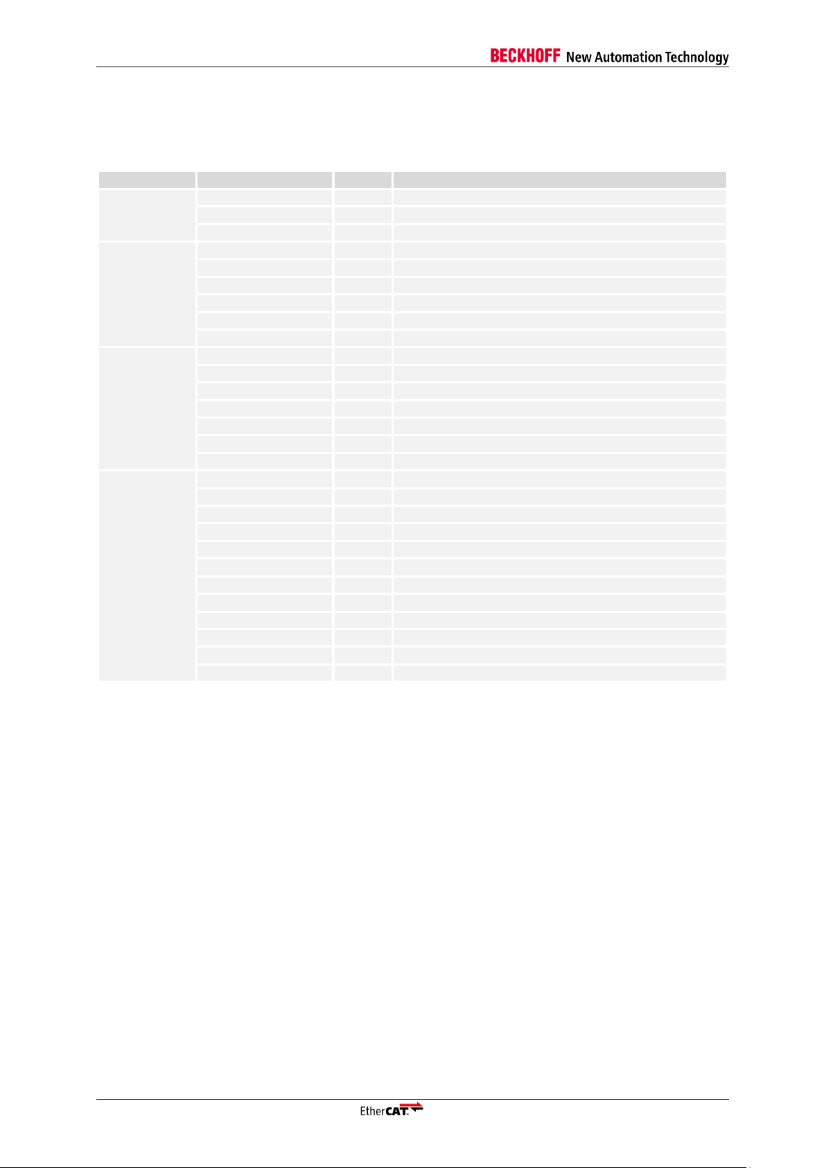
Pin
Pin
Signal
Configuration
Internal
PU/PD
Name
Dir
Name
Dir
21
OSC_IN
I
OSC_IN I
22
OSC_OUT
O
OSC_OUT O
26
RESET
BD
RESET
BD WPU
25
RBIAS
RBIAS
1
TESTMODE
I
TESTMODE
I WPD
Pin
Pin
Signal
Configuration
Internal
PU/PD
Name
Dir
Name
Dir
19
EEPROM_CLK
BD
EEPROM_CLK
BD 3.3 kΩ PU
20
EEPROM_DATA
BD
EEPROM_DATA
BD 3.3 kΩ PU
3.3 General ET1200 Pins
Table 17: General pins
OSC_IN
Connection to external crystal or oscillator input (25 MHz). An oscillator as the clock source for both
ET1200 and the Ethernet PHY is mandatory if an MII port is used and CLK25OUT cannot be used as
the clock source for the PHY. The 25 MHz clock source should have an initial accuracy of 25ppm or
better.
OSC_OUT
Connection to external crystal. Should be left open if an oscillator is connected to OSC_IN.
RESET
The open collector RESET input/output (active low) signals the reset state of ET1200. The reset state
is entered at power-on, if the power supply is to low, or if a reset was initiated using the reset register
0x0040. ET1200 also enters reset state if RESET pin is held low by external devices.
RBIAS
Bias resistor for LVDS TX current adjustment, should be 11 kΩ connected to GND.
TESTMODE
Reserved for testing, should be connected to GND.
3.4 SII EEPROM Interface Pins
Table 18: SII EEPROM pins
EEPROM_CLK
EEPROM I²C clock signal (open collector output).
EEPROM_DATA
EEPROM I²C data signal (open collector output).
Slave Controller – ET1200 Hardware Description III-15
Page 26

Pin Description
Pin
Pin
No MII port used
MII port used
Configuration
Internal
PU/PD
Name
Dir
Signal
Dir
Signal
Dir
47
SYNC/LATCH[0]
BD
SYNC/LATCH[0]
I/O
SYNC/LATCH[0]
I/O
48
SYNC/LATCH[1]/MI_DATA
BD
SYNC/LATCH[1]
I/O
MI_DATA
BD
Pin
Pin
Signal
Configuration
Internal
PU/PD
Name
Dir
Name
Dir
18
RUN/EEPROM_SIZE
BD
RUN O EEPROM_SIZE
WPD
16
LINKACT(0)/MODE[0]
BD
LINKACT(0)
O
MODE[0]
WPD
12
PERR(0)/CLK_MODE[0]
BD
PERR(0)
O
CLK_MODE[0]
WPD
17
LINKACT(1)/MODE[1]
BD
LINKACT(1)
O
MODE[1]
WPD
13
PERR(1)/CLK_MODE[1]
BD
PERR(1)
O
CLK_MODE[1]
WPD
3.5 Distributed Clocks SYNC/LATCH Pins, MII Management Data
Table 19: DC SYNC/LATCH and MII Management pins
SYNC/LATCH[x]/MI_DATA
SYNC/LATCH[x] are Distributed Clocks SyncSignal output or LatchSignal input, depending on SII
EEPROM configuration. If an MII port is used, SYNC/LATCH[1]/MI_DATA becomes MI_DATA, which
is the Ethernet PHY management interface data signal. SYNC/LATCH signals are not driven (high
impedance) until the EEPROM is loaded (MI_DATA is independent of the EEPROM loaded state).
NOTE: MI_DATA must have a pull-up resistor (4.7kΩ recommended for ESCs).
3.6 LED Signals
All LED signals are also used as configuration signals. The polarity of each LED signal depends on
the configuration: LED is active high if pin is pulled down for configuration, and active low if pin is
pulled up. Refer to the example schematics for LED connection details.
Table 20: LED pins
RUN/EEPROM_SIZE
SII EEPROM_SIZE configuration (either 1 Kbit-16 Kbit or 32 Kbit-4 Mbit) sampled at the beginning of
the EEPROM access. Otherwise RUN LED signal, usually. RUN is active high if pin is pulled down,
and active low if pin is pulled up. Refer to example schematics for connection details. RUN LED
should be green.
LINKACT(x)/MODE(x)
Chip MODE configuration pin at power-on, Link/Activity LED output (off=no link, on=link without
activity, blinking=link and activity) for logical port x afterwards. LINKACT(x) is active high if pin is pulled
down, and active low if pin is pulled up. Refer to example schematics for connection details.
Link/Activity LED should be green.
PERR(x)/CLK_MODE(x)
CPU_CLK Mode configuration pin at power-on, Error LED output for logical port x afterwards.
PERR(x) is active high if pin is pulled down, and active low if pin is pulled up. Refer to example
schematics for connection details.
NOTE: PERR(x) LEDs are not part of the EtherCAT indicator specification. They are only intended for testing and
debugging. The PERR(x) LED flashes once if a physical layer receive error occurs. Do not confuse PERR(x)
LEDs with application layer ERR LED, this is not supported by the ESCs and has to be controlled by a
µController.
III-16 Slave Controller – ET1200 Hardware Description
Page 27

Pin Description
Chip mode
SPI
Digital I/O
EBUS bridge
(log. port 3)
MII bridge
(log. port 3)
MODE 00
SPI
+12 Bit GPO
16 Bit I/O
+ control/status
signals
EBUS bridge
+12 Bit GPO
MII bridge
+CLK25OUT +1
Bit GPO
MODE 10/11
SPI
+12 Bit GPO
8 Bit I/O
EBUS bridge +2
Bit GPO
Not available
3.7 Physical Ports and PDI Pins
The ET1200 pin out is optimized in order to achieve an optimum of size and features. To obtain this,
there is a number of pins where either communication or PDI functionality can be assigned to,
depending on the chip mode. The selected chip mode might reduce PDI possibilities
The ET1200 has 18 PDI pins, PDI[17:0]. They are structured in two groups: PDI[7:0] and PDI[17:8].
PDI[7:0] are always available for PDI signals, PDI[17:8] are available for PDI signals in MODE 00, in
MODE 10/11 they are used for MII signals.
Possible Chip mode / PDI combinations
Table 21: Combinations of Chip modes and PDIs
Slave Controller – ET1200 Hardware Description III-17
Page 28

Pin Description
3.7.1 MII Interface LINK_MII(x)
Input signal provided by the PHY if a 100 Mbit/s (Full Duplex) link is established. LINK_MII(x) is active
low.
RX_CLK(x)
MII Receive Clock.
RX_DV(x)
MII receive data valid.
RX_D(x)[3:0]
MII receive data.
RX_ERR(x)
MII receive error.
TX_ENA(x)
MII transmit enable output.
TX_D(x)[3:0]
MII transmit data.
MI_CLK
PHY Management Interface clock.
3.7.1.1 CLK25OUT Signal CLK25OUT
The ET1200 has to provide an Ethernet PHY with a 25 MHz clock signal (CLK25OUT) if a 25 MHz
crystal is used for clock generation. In case a 25 MHz oscillator is used, CLK25OUT is not necessary,
because the Ethernet PHY and the ET1200 can share the oscillator output. CLK25OUT is not
available at PDI[6]/CLK25OUT in chip mode 00 unless the MII bridge port is configured via SII
EEPROM. With the MII bridge port, CLK25OUT is available regardless of C25ENA. For chip modes
10/11, PDI[7] may be configured to deliver CLK25OUT by pulling up the PDI[9]/TX_D[1]/C25ENA
configuration signal.
CLK25OUT provides a clock signal – if configured – during external or ECAT reset, clock output is
only turned off during power-on reset.
3.7.2 EBUS Interface
The EBUS ports of the ET1200 are open failsafe, i.e., the ET1200 detects if an EBUS port is
unconnected and closes the port internally (no physical link).
EBUS(x)-RX+/EBUS(x)-RX-
EBUS LVDS receive signals. EBUS_RX+ pins incorporate a pull-down resistor R
pins incorporate a pull-up resistor R
, even if the pins are not configured for EBUS.
LI-
and EBUS_RX-
LI+
EBUS(x)-TX+/EBUS(x)-TX-
EBUS LVDS transmit signals.
3.7.3 PDI Pins PDI[x]
The function of PDI[x] signals depends on the configuration stored in the device SII EEPROM. PDI
signals are not driven (high impedance) until the EEPROM is loaded. This has to be taken into
account especially for Digital Outputs.
PDI signals are not driven (high impedance) if no PDI is configured (PDI Control register
0x0140=0x00).
III-18 Slave Controller – ET1200 Hardware Description
Page 29

Pin Description
Pin
Pin
Configuration
MODE[1:0]=00
Internal
PU/PD
Name
Dir
Signal
Dir.
36
PDI[8]/TX_D[0]/PHYAD_OFF
BD
PHYAD_OFF
PDI[8]
BD
35
PDI[9]/TX_D[1]/C25_ENA
BD
C25_ENA
PDI[9]
BD
34
PDI[10]/TX_D[2]/C25_SHI[0]
BD
C25_SHI[0]
PDI[10]
BD
33
PDI[11]/TX_D[3]/C25_SHI[1]
BD
C25_SHI[1]
PDI[11]
BD 32
PDI[12]/RX_CLK
BD
PDI[12]
BD
31
PDI[13]/RX_DV
BD
PDI[13]
BD
30
PDI[14]/RX_D[0]
BD
PDI[14]
BD
29
PDI[15]/RX_D[1]
BD
PDI[15]
BD
28
PDI[16]/RX_D[2]
BD
PDI[16]
BD
27
PDI[17]/RX_D[3]
BD
PDI[17]
BD 2
EBUS{1}-RX-/LINK_MII
LI-/I
EBUS(1)-RX-
LI-
27 kΩ PU
3
EBUS{1}-RX+/RX_ERR
LI+/I
EBUS(1)-RX+
LI+
27 kΩ PD
10
EBUS{1}-TX-/MI_CLK
LO-/O
EBUS(1)-TX-
LO-
11
EBUS{1}-TX+/TX_ENA
LO+/O
EBUS(1)-TX+
LO+
8
EBUS{0}-RX-
LI- EBUS(0)-RX-
LI-
27 kΩ PU
9
EBUS{0}-RX+
LI+ EBUS(0)-RX+
LI+
27 kΩ PD
4
EBUS{0}-TX-
LO-
EBUS(0)-TX-
LO-
5
EBUS{0}-TX+
LO+
EBUS(0)-TX+
LO+
Pin
Pin
MODE[1:0]=10
MODE[1:0]=11
Internal
PU/PD
Name
Dir
Signal
Dir.
Signal
Dir.
36
PDI[8]/TX_D[0]/PHYAD_OFF
BD
TX_D(0)[0]
O
TX_D(1)[0]
O
35
PDI[9]/TX_D[1]/C25_ENA
BD
TX_D(0)[1]
O
TX_D(1)[1]
O
34
PDI[10]/TX_D[2]/C25_SHI[0]
BD
TX_D(0)[2]
O
TX_D(1)[2]
O
33
PDI[11]/TX_D[3]/C25_SHI[1]
BD
TX_D(0)[3]
O
TX_D(1)[3]
O
32
PDI[12]/RX_CLK
BD
RX_CLK(0)
I
RX_CLK(1)
I
31
PDI[13]/RX_DV
BD
RX_DV(0)
I
RX_DV(1)
I 30
PDI[14]/RX_D[0]
BD
RX_D(0)[0]
I
RX_D(1)[0]
I
29
PDI[15]/RX_D[1]
BD
RX_D(0)[1]
I
RX_D(1)[1]
I
28
PDI[16]/RX_D[2]
BD
RX_D(0)[2]
I
RX_D(1)[2]
I
27
PDI[17]/RX_D[3]
BD
RX_D(0)[3]
I
RX_D(1)[3]
I
2
EBUS{1}-RX-/LINK_MII
LI-/I
LINK_MII(0)
I
LINK_MII(1)
I
27 kΩ PU
3
EBUS{1}-RX+/RX_ERR
LI+/I
RX_ERR(0)
I
RX_ERR(1)
I
27 kΩ PD
10
EBUS{1}-TX-/MI_CLK
LO-/O
MI_CLK
O
MI_CLK O
11
EBUS{1}-TX+/TX_ENA
LO+/O
TX_ENA(0)
O
TX_ENA(1)
O
8 EBUS{0}-RX-
LI-
EBUS(1)-RX-
LI-
EBUS(0)-RX-
LI-
27 kΩ PU
9
EBUS{0}-RX+
LI+
EBUS(1)-RX+
LI+
EBUS(0)-RX+
LI+
27 kΩ PD
4
EBUS{0}-TX-
LO-
EBUS(1)-TX-
LO-
EBUS(0)-TX-
LO-
5
EBUS{0}-TX+
LO+
EBUS(1)-TX+
LO+
EBUS(0)-TX+
LO+
CPU_CLK
The ET1200 can provide a clock signal for µControllers on pin PDI[7]/CPU_CLK. The CPU_CLK
output setting is controlled by the CLK_MODE configuration pin. If CPU_CLK is enabled, PDI[7] is not
available for the PDI, i.e., I/O[7] is not available for Digital I/O PDI.
CPU_CLK provides a clock signal – if configured – during external or ECAT reset, clock output is only
turned off during power-on reset.
3.7.4 Port 0/1 and PDI[17:8] Signals
Table 22 and Table 23 show the port 0/1 and PDI signals used for ports 0 and 1.
Table 22: Port 0/1 and PDI signals (Configuration and chip mode 00)
Table 23: Port 0/1 and PDI signals (chip modes 10/11)
Slave Controller – ET1200 Hardware Description III-19
Page 30

Pin Description
Pin
Pin
PDI, C25ENA=0,
CLK_MODE=00
PDI, C25ENA=1,
CLK_MODE/=00
Internal
PU/PD
Name
Dir.
Signal
Dir.
Signal
Dir.
46
PDI[0]
BD/LO+
PDI[0]
BD/LO+
PDI[0]
BD/LO+
45
PDI[1]
BD/LO-
PDI[1]
BD/LO-
PDI[1]
BD/LO-
44
PDI[2]
BD/LI+
PDI[2]
BD/LI+
PDI[2]
BD/LI+
27 kΩ PD
43
PDI[3]
BD/LI-
PDI[3]
BD/LI-
PDI[3]
BD/LI-
27 kΩ PU
40
PDI[4]
BD
PDI[4]
BD
PDI[4]
BD 39
PDI[5]
BD
PDI[5]
BD
PDI[5]
BD
38
PDI[6]/CLK25OUT
BD
PDI[6]
BD
CLK25OUT
O
37
PDI[7]/CPU_CLK
BD
PDI[7]
BD
CPU_CLK
O
3.7.5 PDI[7:0] Signals
Table 24 shows the PDI[7:0] signals. The direction of all PDI pins depends on the PDI configuration
stored in the SII EEPROM.
Table 24: PDI pins
3.8 PDI Signal Pinout depending on selected PDI
The PDI signal pinout depends on the selected PDI (SII EEPROM). The PDI selection and PDI signal
pinout is subject to restrictions introduced by the port configuration. Digital I/O and SPI PDI are
available in any configuration – although the I/O width can be reduced depending on the configuration.
The MII bridge port PDIs is only available in chip mode 00.
Refer to PDI descriptions for further PDI and PDI signal descriptions.
The SPI PDI supports additional general purpose output signals, which are not part of the SPI PDI
description:
GPO[x]
General purpose output signals.
III-20 Slave Controller – ET1200 Hardware Description
Page 31

Pin Description
PDI Signal
MODE[1:0]=00
MODE[1:0]=10/11
Signal
Dir.
Signal
Dir.
PDI[0]
I/O[0]
BD
I/O[0]
BD
PDI[1]
I/O[1]
BD
I/O[1]
BD
PDI[2]
I/O[2]
BD
I/O[2]
BD
PDI[3]
I/O[3]
BD
I/O[3]
BD
PDI[4]
I/O[4]
BD
I/O[4]
BD
PDI[5]
I/O[5]
BD
I/O[5]
BD
PDI[6]/CLK25OUT
I/O[6]
BD
I/O[6]
BD
PDI[7]/CPU_CLK
I/O[7]
BD
I/O[7]
BD
PDI[8]
I/O[8]
BD
MII
PDI[9]
I/O[9]
BD
PDI[10]
I/O[10]
BD
PDI[11]
I/O[11]
BD
PDI[12]
I/O[12]
BD
PDI[13]
I/O[14]
BD
PDI[14]
I/O[15]
BD
PDI[15]
I/O[16]
BD
PDI[16]
OUTVALID/WD_TRIG
O
PDI[17]
LATCH_IN/SOF
I/O
PDI Signal
MODE[1:0]=00
MODE[1:0]=10/11
Signal
Dir.
Signal
Dir.
PDI[0]
SPI_CLK
I
SPI_CLK
I
PDI[1]
SPI_SEL
I
SPI_SEL
I
PDI[2]
SPI_DI
I
SPI_DI
I
PDI[3]
SPI_DO
O
SPI_DO
O
PDI[4]
SPI_IRQ
O
SPI_IRQ
O
PDI[5]
EEPROM_LOADED
O
EEPROM_LOADED
O
PDI[6]/CLK25OUT
GPO[0]
O
GPO[0]
O
PDI[7]/CPU_CLK
GPO[1]
O
GPO[1]
O
PDI[8]
GPO[2]
O
MII
PDI[9]
GPO[3]
O
PDI[10]
GPO[4]
O
PDI[11]
GPO[5]
O
PDI[12]
GPO[6]
O
PDI[13]
GPO[7]
O
PDI[14]
GPO[8]
O
PDI[15]
GPO[9]
O
PDI[16]
GPO[10]
O
PDI[17]
GPO[11]
O
3.8.1 Digital I/O Pin Out
Table 25: Mapping of Digital I/O Interface
3.8.2 SPI Pin Out
Table 26: Mapping of SPI Interface
Slave Controller – ET1200 Hardware Description III-21
Page 32
Pin Description
PDI Signal
MODE[1:0]=00
MODE[1:0]=10/11
Signal
Dir.
Signal
Dir.
PDI[0]
EBUS(3)_TX+
LO+
EBUS(3)_TX+
LO+
PDI[1]
EBUS(3)_TX-
LO-
EBUS(3)_TX-
LO-
PDI[2]
EBUS(3)_RX+
LI+
EBUS(3)_RX+
LI+
PDI[3]
EBUS(3)_RX-
LI-
EBUS(3)_RX-
LI-
PDI[4]
PERR(3)
O
PERR(3)
O
PDI[5]
LINKACT(3)
O
LINKACT(3)
O
PDI[6]/CLK25OUT
GPO[0]
O
GPO[0]
O
PDI[7]/CPU_CLK
GPO[1]
O
GPO[1]
O
PDI[8]
GPO[2]
O
MII
PDI[9]
GPO[3]
O
PDI[10]
GPO[4]
O
PDI[11]
GPO[5]
O
PDI[12]
GPO[6]
O
PDI[13]
GPO[7]
O
PDI[14]
GPO[8]
O
PDI[15]
GPO[9]
O
PDI[16]
GPO[10]
O
PDI[17]
GPO[11]
O
PDI Signal
MODE[1:0]=00
Signal
Dir.
PDI[0]
TX_ENA(3)
O
PDI[1]
MI_CLK
O
PDI[2]
RX_ERR(3)
I
PDI[3]
LINK_MII(3)
I
PDI[4]
PERR(3)
O
PDI[5]
LINKACT(3)
O
PDI[6]/CLK25OUT
CLK25OUT
O
PDI[7]/CPU_CLK
GPO[1]
O
PDI[8]
TX_D(3)[0]
O
PDI[9]
TX_D(3)[1]
O
PDI[10]
TX_D(3)[2]
O
PDI[11]
TX_D(3)[3]
O
PDI[12]
RX_CLK(3)
I
PDI[13]
RX_DV(3)
I
PDI[14]
RX_D(3)[0]
I
PDI[15]
RX_D(3)[1]
I
PDI[16]
RX_D(3)[2]
I
PDI[17]
RX_D(3)[3]
I
3.8.3 EBUS/MII bridge port (Logical port 3)
The bridge port is an additional port with logical number 3, it is configured via SII EEPROM, thus it is
not available directly after power-on. The bridge port becomes available once the EEPROM is loaded
successfully. The loop at this port is initially closed and has to be opened by the master explicitly. The
bridge port may be either EBUS or MII. The MII bridge port is only available in chip mode 00.
The polarity of PERR(3) and LINKACT(3) is active high.
Table 27: Mapping of EBUS Bridge signals
Table 28: Mapping of MII Bridge signals
III-22 Slave Controller – ET1200 Hardware Description
Page 33
Pin Description
V
CC VCC I/O
V
CC Core/VCC PLL
Input signals
Output signals
Comment
3.3V
External 3.3V
(= VCC)
Internal LDO
(2.5V)
3.3V only
3.3V only
Single power
supply, low power
dissipation
3.3V
External 3.3V
(= VCC)
External 2.5V
3.3V only
3.3V only
Dual power supply,
lowest power
dissipation
5V
Internal LDO
(3.3V)
Internal LDO
(2.5V)
3.3V only
3.3V only
Single power
supply, highest
power dissipation
5V
Internal LDO
(3.3V)
External 2.5V
3.3V only
3.3V only
Dual power supply
Not recommended:
5V
External 5V
(= VCC)
Internal LDO
(2.5V)
5V only
5V only
Single power
supply, high power
dissipation
5V
External 5V
(= VCC)
External 2.5V
5V only
5V only
Dual power supply,
high power
dissipation
Pin
Pin name
EP
GND
14
VCC
15
GND
6
V
CC I/O
7
GND
I/O
41
V
CC Core
(2.5V)
42
GND
Core
24
V
CC PLL
(2.5V)
23
GND
PLL
3.9 Power Supply
The ET1200 supports different power supply and I/O voltage options with 3.3V (or 5V I/O, not
recommended) and optionally single or dual power supply.
The V
V
CCI/O
supply voltage directly determines the I/O voltages for all inputs and outputs, i.e., with 3.3V
CCI/O
, the inputs are 3.3V I/O compliant and they are not 5V tolerant (V
has to be 5V if 5V tolerant
CCI/O
I/Os are required).
Two internal LDOs generate the I/O supply voltage V
V
CC Core/VCC PLL
than V
CC I/O
(nom. 2.5V) from the ET1200 power supply input VCC. VCC must be equal or greater
, and V
is always equal to V
CC PLL
. The internal LDOs cannot be switched off, they
CC Core
(nom. 3.3V) and the core supply voltages
CC I/O
stop operating if the external supply voltage is higher than the internal LDO output voltage, thus
external supply voltages have to be higher (at least 0.1V) than the internal LDO output voltages.
Using the internal LDOs increases power dissipation, and power consumption for 5V I/O voltage is
significantly higher than power consumption for 3.3V I/O. It is highly recommended to use 3.3V I/O
voltage and the internal LDO for V
CC Core/VCC PLL
For 3.3V I/O with external 3.3V power supply, both VCC and V
external 3.3V supply voltage, and for 5V I/O voltage, both VCC and V
.
have to be connected to the
CCI/O
have to be connected to the
CCI/O
external 5V supply voltage.
Voltage stabilization capacitors at all power pairs are necessary.
Table 29: Power supply options (all voltages nomal)
Table 30: Power supply
Slave Controller – ET1200 Hardware Description III-23
Page 34
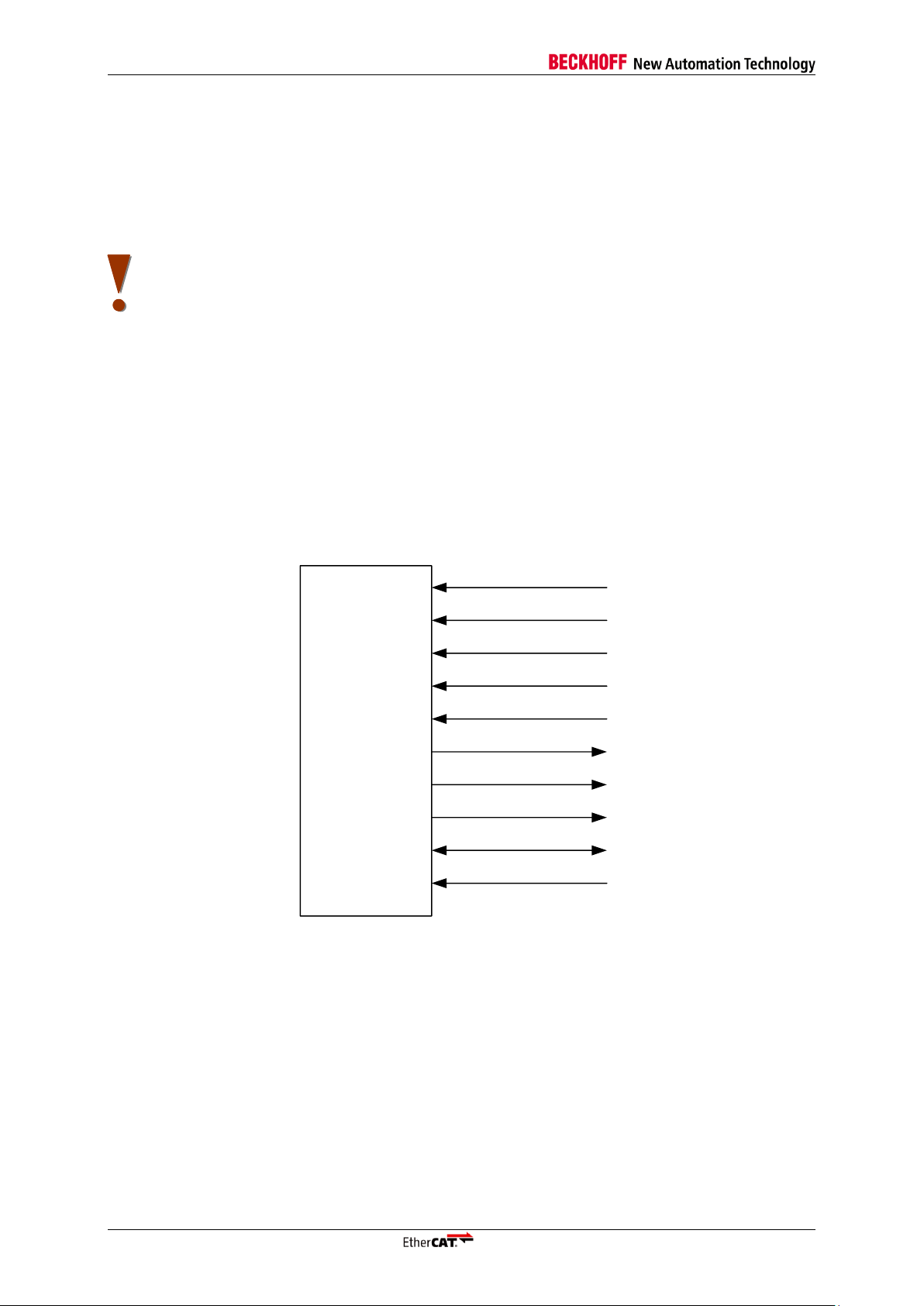
MII Interface
EtherCAT
device
RX_CLK
LINK_MII
RX_DV
RX_ERR
RX_D[3:0]
TX_ENA
MI_CLK
TX_D[3:0]
MI_DATA
PHYAD_OFF
4 MII Interface
The ET1200 is connected with Ethernet PHYs using the MII interface. The MII interface of the ET1200
is optimized for low processing/forwarding delays by omitting a transmit FIFO. To allow this, the
ET1200 has additional requirements to Ethernet PHYs, which are easily accomplished by several PHY
vendors.
Refer to “Section I – Technology” for Ethernet PHY requirements.
Additional information regarding the ET1200:
The clock source of the PHYs is either CLK25OUT of the ET1200, or the clock signal that is
connected to OSC_IN if a quartz oscillator is used.
The signal polarity of LINK_MII is not configurable, LINK_MII has to be active low.
The TX_CLK signal of the PHYs is not connected to the ET1200. The ET1200 does not use the
MII interface for link detection or link configuration.
For details about the ESC MII Interface refer to Section I.
4.1 MII Interface Signals
The MII interface of the ET1200 has the following signals:
Figure 3: MII Interface signals
III-24 Slave Controller – ET1200 Hardware Description
Page 35

MII Interface
Signal
Direction
Description
LINK_MII
IN
Input signal provided by the PHY if a 100 Mbit/s
(Full Duplex) link is established
RX_CLK
IN
Receive Clock
RX_DV
IN
Receive data valid
RX_D[3:0]
IN
Receive data (alias RXD)
RX_ERR
IN
Receive error (alias RX_ER)
TX_ENA
OUT
Transmit enable (alias TX_EN)
TX_D[3:0]
OUT
Transmit data (alias TXD)
MI_CLK
OUT
Management Interface clock (alias MCLK)
MI_DATA
BIDIR
Management Interface data (alias MDIO)
PHYAD_OFF
IN
Configuration: PHY address offset
Table 31: MII Interface signals
MI_DATA must have an external pull-up resistor (4.7 kΩ recommended for ESCs). MI_CLK is driven
rail-to-rail, idle value is High.
4.2 PHY Address Configuration
The ET1200 addresses Ethernet PHYs using logical port number (or PHY address register value) plus
PHY address offset. Typically, the Ethernet PHY addresses should correspond with the logical port
number, so PHY addresses 0-3 are used.
A PHY address offset of 16 can be applied which moves the PHY addresses to 16-19 by inverting the
MSB of the PHY address internally.
If both alternatives cannot be used, the PHYs should be configured to use an actual PHY address
offset of 1, i.e., PHY addresses 1-4. The PHY address offset configuration of the ET1200 remains 0.
Refer to Section I for more details about PHY addressing.
Slave Controller – ET1200 Hardware Description III-25
Page 36
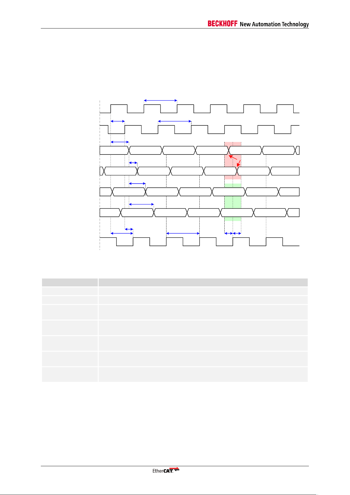
MII Interface
OSC_IN
CLK25Out
TX_CLK
TX_ENA
TX_D[3:0]
t
Clk25Out
TX_ENA
TX_D[3:0]
TX_ENA
TX_D[3:0]
TX_ENA
TX_D[3:0]
TX_ENA
TX_D[3:0]
TX_ENA
TX_D[3:0]
TX_ENA
TX_D[3:0]
TX_ENA
TX_D[3:0]
TX_ENA
TX_D[3:0]
TX_ENA
TX_D[3:0]
TX_ENA
TX_D[3:0]
TX_ENA
TX_D[3:0]
TX_ENA
TX_D[3:0]
TX_ENA
TX_D[3:0]
TX_ENA
TX_D[3:0]
TX_ENA
TX_D[3:0]
t
CLK25
t
PHY_TX_CLK_delay
10 ns
20 ns
30 ns
t
PHY_TX_hold
t
PHY_TX_setup
Wrong: Setup/Hold Timing violated
Good: Setup/Hold Timing met
t
CLK25
t
CLK25
t
PHY_TX_CLK_delay_OSC
TX_ENA, TX_D[3:0]
TX_Shift[1:0]=00
TX_ENA, TX_D[3:0]
TX_Shift[1:0]=01
TX_ENA, TX_D[3:0]
TX_Shift[1:0]=10
TX_ENA, TX_D[3:0]
TX_Shift[1:0]=11
t
TX_delay
Parameter
Comment
t
CLK25
25 MHz clock source (OSC_IN, see f
CLK25
)
t
CLK25OUT
CLK25OUT delay after OSC_IN (refer to AC characteristics)
t
TX_delay
TX_ENA/TX_DATA[3:0] delay after rising edge of OSC_IN (refer to AC
characteristics)
t
PHY_TX_CLK_delay
Delay between PHY clock source CLK25OUT and TX_CLK output of the
PHY, PHY dependent
t
PHY_TX_CLK_delay_OSC
Delay between PHY clock source OSC_IN and TX_CLK output of the PHY,
PHY dependent
t
PHY_TX_setup
PHY setup requirement: TX_ENA/TX_DATA with respect to TX_CLK (PHY
dependent, IEEE802.3 limit is 15 ns)
t
PHY_TX_hold
PHY hold requirement: TX_ENA/TX_DATA with respect to TX_CLK (PHY
dependent, IEEE802.3 limit is 0 ns)
4.3 TX Shift Compensation
Since ET1200 and the Ethernet PHY share the same clock source, TX_CLK from the PHY has a fixed
phase relation to TX_ENA/TX_D[3:0]from the ET1200. Thus, TX_CLK is not connected and the delay
of a TX FIFO inside the ET1200 is saved. The phase shift between TX_CLK and TX_ENA/TX_D[3:0]
can be compensated by an appropriate value for TX Shift, which will delay TX_ENA/ TX_D[3:0] by 0,
10, 20, or 30 ns.
NOTE: TX Shift can be adjusted by displaying TX_CLK of a PHY and TX_ENA/TX_D[3:0] on an oscilloscope.
TX_ENA/TX_D is allowed to change between 0 ns and 25 ns after a rising edge of TX_CLK (according to
IEEE802.3 – check your PHY’s documentation, it may contain relaxed timing requirements). Configure TX Shift so
that TX_ENA/TX_D[3:0] change near the middle of this range. It is sufficient to check just one of the
TX_ENA/TX_D[3:0] signals, because they are nearly generated at the same time.
Figure 4: TX Shift Timing Diagram
Table 32: TX Shift Timing characteristics
III-26 Slave Controller – ET1200 Hardware Description
Page 37
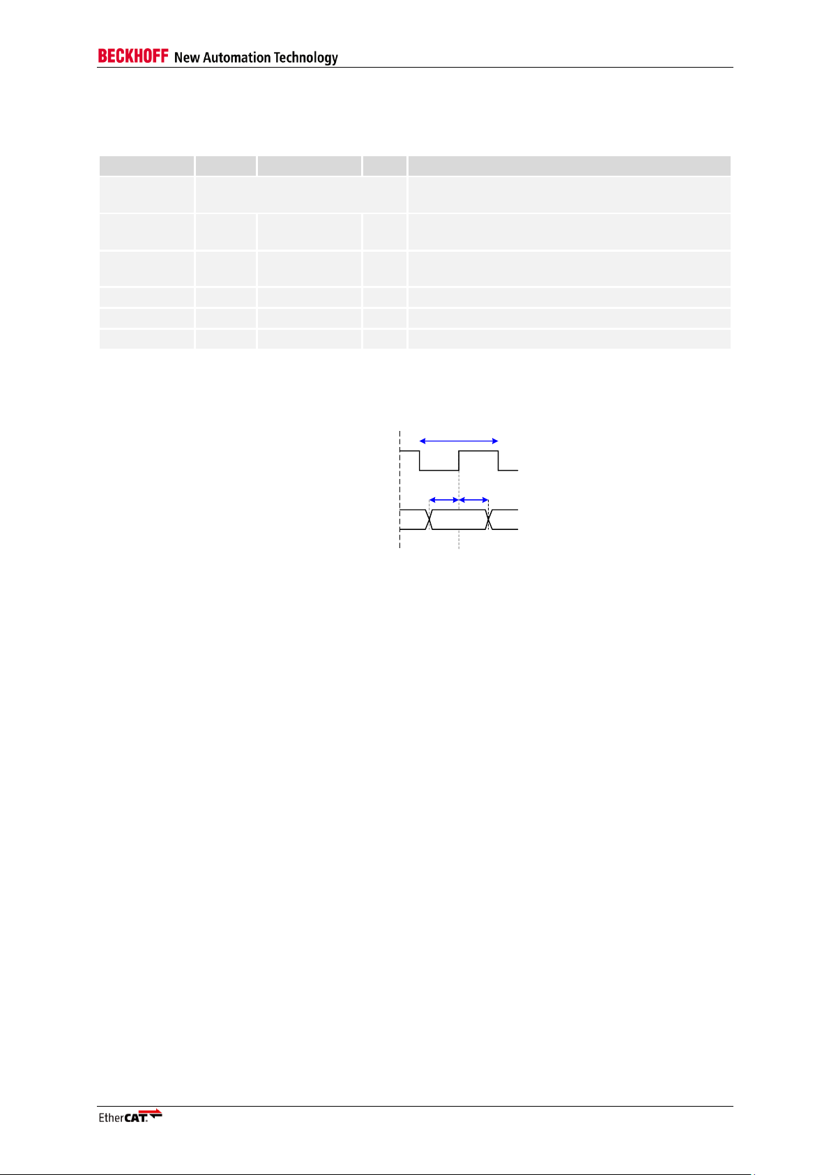
MII Interface
Parameter
Min
Typ
Max
Comment
t
RX_CLK
40 ns ± 100 ppm
RX_CLK period (100 ppm with maximum FIFO
Size only)
t
RX_setup
6
RX_DV/RX_DATA/RX_D[3:0] valid before rising
edge of RX_CLK
t
RX_hold
5
RX_DV/RX_DATA/RX_D[3:0] valid after rising
edge of RX_CLK
t
Clk
~ 1.44 µs
MI_CLK period (f
Clk
≈ 700 kHz)
t
Write
~ 92.16 µs
MI Write access time
t
Read
~ 91.44 us
MI Read access time
RX_DV
RX_D[3:0]
RX_ERR
RX_CLK
t
RX_setup
t
RX_hold
RX signals valid
t
RX_CLK
4.4 Timing specifications
Table 33: MII timing characteristics
NOTE: For MI timing diagrams refer to Section I.
Figure 5: MII timing RX signals
Slave Controller – ET1200 Hardware Description III-27
Page 38
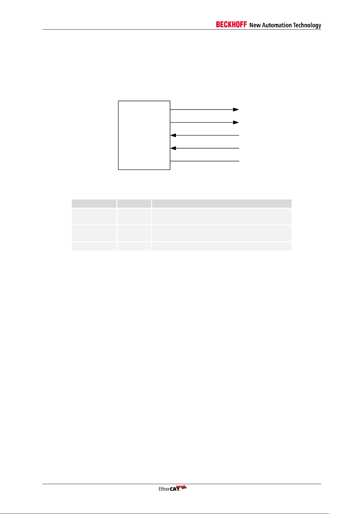
EBUS/LVDS Interface
EtherCAT
device
EBUS-TX-
EBUS-TX+
EBUS-RX+
EBUS-RX-
RBIAS
Signal
Direction
Description
EBUS-TX+
EBUS-TX-
OUT
EBUS/LVDS transmit signals
EBUS-RX+
EBUS-RX-
IN
EBUS/LVDS receive signals.
RBIAS
BIAS resistor for EBUS-TX current adjustment
5 EBUS/LVDS Interface
For details about the ESC EBUS Interface refer to Section I.
5.1 EBUS Interface Signals
The EBUS interface of the ET1200 has the following signals:
Figure 6: EBUS Interface Signals
Table 34: EBUS Interface signals
NOTE: An external LVDS termination with an impedance of 100 Ω between EBUS-RX+ and EBUS-RX- is
necessary for EBUS ports. EBUS-RX+ incorporates a pull-down resistor and EBUS-RX- incorporated a pull-up
resistor.
III-28 Slave Controller – ET1200 Hardware Description
Page 39
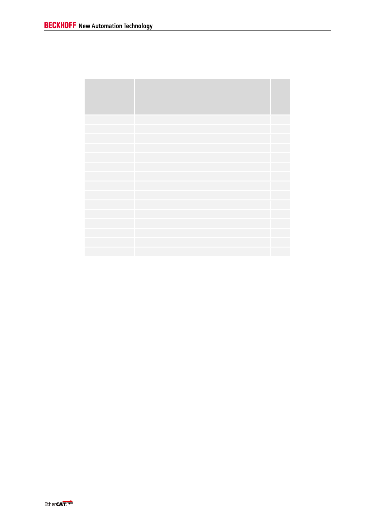
PDI Description
PDI number
(PDI Control
register
0x0140[7:0])
PDI name
ET1200
0
Interface deactivated
x 4 Digital I/O x 5
SPI Slave x 7
EtherCAT Bridge (port 3)
x 8 16 Bit async. µC
9 8 Bit async. µC
10
16 Bit sync. µC
11
8 Bit sync. µC
16
32 Digital Input/0 Digital Output
17
24 Digital Input/8 Digital Output
18
16 Digital Input/16 Digital Output
19
8 Digital Input/24 Digital Output
20
0 Digital Input/32 Digital Output
128
On-chip bus (Avalon or OPB)
Others
Reserved
6 PDI Description
Table 35: Available PDIs for ET1200
6.1 PDI Deactivated
The PDI is deactivated with PDI type 0x00. The PDI pins are not driven (high impedance).
Slave Controller – ET1200 Hardware Description III-29
Page 40
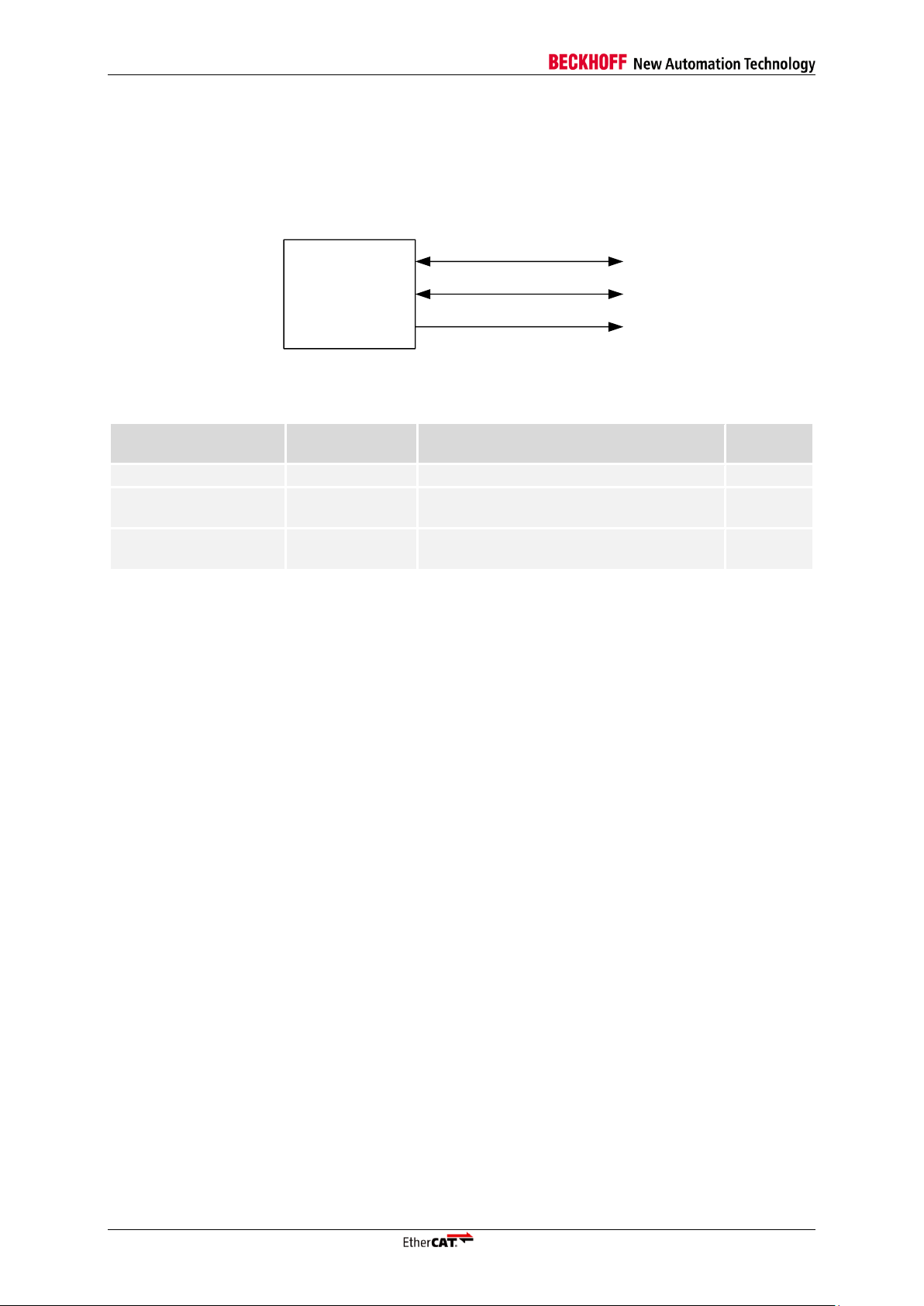
PDI Description
ET1200
I/O[15:0]
LATCH_IN/SOF
OUTVALID/WD_TRIG
Signal
Direction
Description
Signal
polarity
I/O[15:0]
IN/OUT/BIDIR
Input/Output or Bidirectional data
LATCH_IN/SOF
IN/OUT
External data latch signal or Start of
Frame
act. high
OUTVALID/WD_TRIG
OUT
Output data is valid/Output event or
Watchdog Trigger
act. high
6.2 Digital I/O Interface
6.2.1 Interface
The Digital I/O PDI is selected with PDI type 0x04. The signals of the Digital I/O interface are:
Figure 7: ET1200 Digital I/O Signals
Table 36: ET1200 Digital I/O signals
NOTE: Unsupported control signals OE_EXT and OE_CONF are assumed to be high.
6.2.2 Configuration
The Digital I/O interface is selected with PDI type 0x04 in the PDI control register 0x0140. It supports
different configurations, which are located in registers 0x0150 – 0x0153.
6.2.3 Digital Inputs
Digital input values appear in the process memory at address 0x1000:0x1003. EtherCAT devices use
Little Endian byte ordering, so I/O[7:0] can be read at 0x1000 etc. Digital inputs are written to the
process memory by the Digital I/O PDI using standard PDI write operations.
Digital inputs can be configured to be sampled by the ESC in four ways:
Digital inputs are sampled at the start of each Ethernet frame, so that EtherCAT read commands
to address 0x1000:0x1003 will present digital input values sampled at the start of the same frame.
The SOF signal can be used externally to update the input data, because the SOF is signaled
before input data is sampled.
The sample time can be controlled externally by using the LATCH_IN signal. The input data is
sampled by the ESC each time a rising edge of LATCH_IN is recognized.
Digital inputs are sampled at Distributed Clocks SYNC0 events.
Digital inputs are sampled at Distributed Clocks SYNC1 events.
For Distributed Clock SYNC input, SYNC generation must be activated (register 0x0981). SYNC
output is not necessary (register 0x0151). SYNC pulse length (registers 0x0982:0x0983) should not be
set to 0, because acknowledging of SYNC events is not possible with Digital I/O PDI. Sample time is
the beginning of the SYNC event.
III-30 Slave Controller – ET1200 Hardware Description
Page 41
PDI Description
16
Output register
Digital I/O output
data register
0x0F00:0x0F01
Digital output pins
16
16 16
EOF
DC Sync0
DC Sync1
D Q
&
Output event
configuration
Watchdog
&
Output event occured
since watchdog active
6.2.4 Digital Outputs
Digital Output values have to be written to register 0x0F00:0x0F03 (register 0x0F00 controls I/O[7:0]
etc.). Digital Output values are not read by the Digital I/O PDI using standard read commands,
instead, there is a direct connection for faster response times.
The process data watchdog (register 0x0440) has to be either active or disabled; otherwise digital
outputs will not be updated. Digital outputs can be configured to be updated in four ways:
Digital Outputs are updated at the end of each EtherCAT frame (EOF mode).
Digital outputs are updated with Distributed Clocks SYNC0 events (DC SYNC0 mode).
Digital outputs are updated with Distributed Clocks SYNC1 events (DC SYNC1 mode).
Digital Outputs are updated at the end of an EtherCAT frame which triggered the Process Data
Watchdog (with typical SyncManager configuration: a frame containing a write access to at least
one of the registers 0x0F00:0x0F03). Digital Outputs are only updated if the EtherCAT frame was
correct (WD_TRIG mode).
For Distributed Clock SYNC output, SYNC generation must be activated (register 0x0981). SYNC
output is not necessary (register 0x0151). SYNC pulse length (registers 0x0982:0x0983) should not be
set to 0, because acknowledging of SYNC events is not possible with Digital I/O PDI. Output time is
the beginning of the SYNC event.
An output event is always signaled by a pulse on OUTVALID even if the digital outputs remain
unchanged.
For output data to be visible on the I/O signals, the following conditions have to be met:
SyncManager watchdog must be either active (triggered) or disabled.
Output values have to be written to the registers 0x0F00:0x0F03 within a valid EtherCAT frame.
The configured output update event must have occurred.
Figure 8: Digital Output Principle Schematic
NOTE: The Digital Outputs are not driven (high impedance) until the EEPROM is loaded. The Digital Outputs are
also not driven if the Watchdog is expired. This behavior has to be taken into account when using digital output
signals.
Slave Controller – ET1200 Hardware Description III-31
Page 42

PDI Description
EtherCAT
device
Digital Input
Digital Output
DATA
R
OUTVALID
C1
1D Q
D-FF
6.2.5 Bidirectional mode
In bidirectional mode, all DATA signals are bidirectional (individual input/output configuration is
ignored). Input signals are connected to the ESC via series resistors, output signals are driven actively
by the ESC. Output signals are permanently available if they are latched with OUTVALID (Flip-Flop or
Latch).
Figure 9: Bidirectional mode: Input/Output connection (R=4.7 kΩ recommended)
Input sample event and output update event can be configured as described in the Digital
Inputs/Digital Outputs chapter.
An output event is signaled by a pulse on OUTVALID even if the digital outputs remain unchanged.
Overlapping input and output events will lead to corrupt input data.
6.2.6 Output Driver
The output drivers for the digital I/O signals of the ET1200 are active while the SyncManager
watchdog is active (triggered) or disabled, otherwise the output driver is disabled (high impedance).
6.2.7 SyncManager Watchdog
The SyncManager watchdog (registers 0x0440:0x0441) must be either active (triggered) or disabled
for output values to appear on the I/O signals. The SyncManager Watchdog is triggered by an
EtherCAT write access to the output data registers.
If the output data bytes are written independently, a SyncManager with a length of 1 byte is used for
each byte of 0x0F00:0x0F03 containing output bits (SyncManager N configuration: buffered mode,
EtherCAT write/PDI read, and Watchdog Trigger enabled: 0x44 in register 0x0804+N*8). Alternatively,
if all output data bits are written together in one EtherCAT command, one SyncManager with a length
of 1 byte is sufficient (SyncManager N configuration: buffered mode, EtherCAT write/PDI read, and
Watchdog Trigger enabled: 0x44 in register 0x0804+N*8). The start address of the SyncManager
should be one of the 0x0F00:0x0F03 bytes containing output bits, e.g., the last byte containing output
bits.
The SyncManager Watchdog can also be disabled by writing 0 into registers 0x0440:0x0441.
The Watchdog Mode configuration bit is used to configure if the expiration of the SyncManager
Watchdog will have an immediate effect on the I/O signals (output reset immediately after watchdog
timeout) or if the effect is delayed until the next output event (output reset with next output event). The
latter case is especially relevant for Distributed Clock SYNC output events, because any output
change will occur at the configured SYNC event.
Immediate output reset after watchdog timeout is not available if OUTVALID mode set to watchdog
trigger (0x0150[1]=1).
For external watchdog implementations, the WD_TRIG (watchdog trigger) signal can be used. A
WD_TRIG pulse is generated if the SyncManager Watchdog is triggered. In this case, the internal
SyncManager Watchdog should be disabled. For devices without the WD_TRIG signal, OUTVALID
can be configured to reflect WD_TRIG.
III-32 Slave Controller – ET1200 Hardware Description
Page 43

PDI Description
Parameter
Min
Max
Comment
t
DATA_setup
8 ns
Input data valid before LATCH_IN
t
DATA_hold
4 ns
Input data valid after LATCH_IN
t
LATCH_IN
8 ns
LATCH_IN high time
t
SOF
35 ns
45 ns
SOF high time
t
SOF_to_DATA_setup
1,2 µs
Input data valid after SOF, so that Inputs
can be read in the same frame
t
SOF_to_DATA_hold
1,6 µs
Input data invalid after SOF
t
input_event_delay
440 ns
Time between consecutive input events
t
OUTVALID
75 ns
85 ns
OUTVALID high time
t
DATA_to_OUTVALID
65 ns
Output data valid before OUTVALID
t
WD_TRIG
35 ns
45 ns
WD_TRIG high time
t
DATA_to_WD_TRIG
35 ns
Output data valid after WD_TRIG
t
OE_EXT_to_DATA_invalid
- - Not applicable for ET1200
t
output_event_delay
320 ns
Time between consecutive output events
t
BIDIR_DATA_valid
65 ns
Bidirectional mode: I/O valid before
OUTVALID
t
BIDIR_DATA_invalid
65 ns
Bidirectional mode: I/O invalid after
OUTVALID
t
BIDIR_event_delay
440 ns
Bidirectional mode: time between
consecutive input or output events
6.2.8 SOF
SOF indicates the start of an Ethernet/EtherCAT frame. It is asserted shortly after RX_DV=1 or EBUS
SOF. Input data is sampled in the time interval between t
SOF_to_DATA_setup
and t
SOF_to_DATA_setup
after the
SOF signal is asserted.
6.2.9 OUTVALID
A pulse on the OUTVALID signal indicates an output event. If the output event is configured to be the
end of a frame, OUTVALID is issued shortly after RX_DV=0 or EBUS EOF, right after the CRC has
been checked and the internal registers have taken their new values. OUTVALID is issued
independent of actual output data values, i.e., it is issued even if the output data does not change.
6.2.10 Timing specifications
Table 37: Digital I/O timing characteristics ET1200
Slave Controller – ET1200 Hardware Description III-33
Page 44

PDI Description
SOF
DATA
Input DATA
t
SOF_to_DATA_setup
t
SOF
t
SOF_to_DATA_hold
LATCH_IN
DATA
Input DATA
t
DATA_hold
t
DATA_setup
t
LATCH_IN
t
Input_event_delay
OUTVALID
DATA
t
DATA_to_OUTVALID
Output DATA
t
OUTVALID
Zero or High-Impedance
t
OE_EXT_to_DATA_invalid
OE_EXT
WD_TRIG
t
WD_TRIG
t
DATA_to_WD_TRIG
t
output_event_delay
OUTVALID
DATA
Input data
t
BIDIR_DATA_valid
Input data
t
BIDIR_DATA_invalid
t
OUTVALID
Input events
t
BIDIR_event_delay
Output data
t
BIDIR_event_delay
Input events
allowed
Input events
allowed
No input events allowed
Figure 10: Digital Input: Input data sampled at SOF, I/O can be read in the same frame
Figure 11: Digital Input: Input data sampled with LATCH_IN
III-34 Slave Controller – ET1200 Hardware Description
Figure 12: Digital Output timing
Figure 13: Bidirectional Mode timing
Page 45

PDI Description
SPI master
(µController)
SPI_SEL
SPI_CLK
SPI_DI
SPI_DO
SPI_IRQ
SPI slave
(EtherCAT
device)
EEPROM_LOADED
Signal
Direction
Description
Signal polarity
SPI_SEL
IN (master → slave)
SPI chip select
Typical: act. low
SPI_CLK
IN (master → slave)
SPI clock
SPI_DI
IN (master → slave)
SPI data MOSI
act. high
SPI_DO
OUT (slave → master)
SPI data MISO
act. high
SPI_IRQ
OUT (slave → master)
SPI interrupt
Typical: act. low
EEPROM_LOADE
D
OUT (slave → master)
PDI is active, EEPROM is
loaded
act. high
6.3 SPI Slave Interface
6.3.1 Interface
An EtherCAT device with PDI type 0x05 is an SPI slave. The SPI has 5 signals: SPI_CLK, SPI_DI
(MOSI), SPI_DO (MISO), SPI_SEL and SPI_IRQ:
Figure 14: SPI master and slave interconnection
Table 38: SPI signals
6.3.2 Configuration
The SPI slave interface is selected with PDI type 0x05 in the PDI control register 0x0140. It supports
different timing modes and configurable signal polarity for SPI_SEL and SPI_IRQ. The SPI
configuration is located in register 0x0150.
NOTE: The maximum SPI_CLK frequency depends on the SPI mode (ET1200 only).
6.3.3 SPI access
Each SPI access is separated into an address phase and a data phase. In the address phase, the SPI
master transmits the first address to be accessed and the command. In the data phase, read data is
presented by the SPI slave (read command) or write data is transmitted by the master (write
command). The address phase consists of 2 or 3 bytes depending on the address mode. The number
of data bytes for each access may range from 0 to N bytes. The slave internally increments the
address for the following bytes after reading or writing the start address. The bits of both
address/command and data are transmitted in byte groups.
The master starts an SPI access by asserting SPI_SEL and terminates it by taking back SPI_SEL
(polarity determined by configuration). While SPI_SEL is asserted, the master has to cycle SPI_CLK
eight times for each byte transfer. In each clock cycle, both master and slave transmit one bit to the
other side (full duplex). The relevant edges of SPI_CLK for master and slave can be configured by
selecting SPI mode and Data Out sample mode.
The most significant bit of a byte is transmitted first, the least significant bit last, the byte order is low
byte first. EtherCAT devices use Little Endian byte ordering.
Slave Controller – ET1200 Hardware Description III-35
Page 46

PDI Description
CMD[2]
CMD[1]
CMD[0]
Command
0 0 0
NOP (no operation)
0 0 1
reserved
0 1 0
Read 0 1
1
reserved
1 0 0
Write 1 0
1
reserved
1 1 0
Address Extension (3 address/command bytes)
1 1 1
reserved
Byte
2 Byte address mode
3 Byte address mode
0
A[12:5] address bits [12:5]
A[12:5] address bits [12:5]
1
A[4:0] address bits [4:0]
CMD0[2:0] read/write command
A[4:0] address bits [4:0]
CMD0[2:0] 3 byte addressing: 110b
2
D0[7:0] data byte 0
A[15:13] address bits [15:13]
CMD1[2:0] read/write command
res[1:0] two reserved bits, set to 00b
3
D1[7:0] data byte 1
D0[7:0] data byte 0
4 ff.
D2[7:0] data byte 2
D1[7:0] data byte 1
Byte
2 Byte address mode
3 Byte address mode
SPI_DI
(MOSI)
SPI_DO
(MISO)
SPI_DI
(MOSI)
SPI_DO
(MISO)
0
A[12:5]
I0[7:0] interrupt request
register 0x0220
A[12:5]
I0[7:0] interrupt request register
0x0220
1
A[4:0]
CMD0[2:0]
I1[7:0] interrupt request
register 0x0221
A[4:0]
CMD0[2:0]
I1[7:0] interrupt request register
0x0221
2
(Data phase)
A[15:13]
CMD1[2:0]
I2[7:0] interrupt request register
0x0222
6.3.4 Commands
The command CMD0 in the second address/command byte may be READ, WRITE, NOP, or Address
Extension. The command CMD1 in the third address/command byte may have the same values:
Table 39: SPI commands CMD0 and CMD1
6.3.5 Address modes
The SPI slave interface supports two address modes, 2 byte addressing and 3 byte addressing. With
two byte addressing, the lower 13 address bits A[12:0] are selected by the SPI master, while the upper
3 bits A[15:13] are assumed to be 000b inside the SPI slave, thus only the first 8 Kbyte in the
EtherCAT slave address space can be accessed. Three byte addressing is used for accessing the
whole 64 Kbyte address space of an EtherCAT slave.
Table 40: Address modes
6.3.6 Interrupt request register (AL Event register)
During the address phase, the SPI slave transmits the PDI interrupt request registers 0x0220-0x0221
(2 byte address mode), and additionally register 0x0222 for 3 byte addressing on SPI_DO (MISO):
Table 41: Interrupt request register transmission
III-36 Slave Controller – ET1200 Hardware Description
Page 47

PDI Description
6.3.7 Write access
In the data phase of a write access, the SPI master sends the write data bytes to the SPI slave
(SPI_DI/MOSI). The write access is terminated by taking back SPI_SEL after the last byte. The
SPI_DO signal (MISO) is undetermined during the data phase of write accesses.
6.3.8 Read access
In the data phase of a read access, the SPI slave sends the read data bytes to the SPI master
(SPI_DO/MISO).
6.3.8.1 Read Wait State
Between the last address phase byte and the first data byte of a read access, the SPI master has to
wait for the SPI slave to fetch the read data internally. Subsequent read data bytes are prefetched
automatically, so no further wait states are necessary.
The SPI master can choose between these possibilities:
The SPI master may either wait for the specified worst case internal read time t
after the last
read
address/command byte and before the first clock cycle of the data phase.
The SPI master may use the BUSY signaling of the SPI slave to achieve faster read times. The
SPI slave presents its state on SPI_DO (MISO) after SPI_DI (MOSI) is set high between address
and data phase (Busy Out enable) until SPI_DI is set to low (Busy Out enable is edge sensitive) .
While the SPI slave is busy, it will drive SPI_DO high. Once it has finished, SPI_DO is set to low
and the master may start with the next clock cycle for the first read data byte.
BUSY signaling is not available in SPI mode 0/2 with normal data out sample.
6.3.8.2 Read Termination
The SPI_DI signal (MOSI) is used for termination of the read access by the SPI master. For the last
data byte, the SPI master has to set SPI_DI to high (Read Termination byte = 0xFF), so the slave will
not prefetch the next read data internally. If SPI_DI is low during a data byte transfer, at least one
more byte will be read by the master afterwards.
6.3.9 SPI access errors and SPI status flag
The following reasons for SPI access errors are detected by the SPI slave:
The number of clock cycles recognized while SPI_SEL is asserted is not a multiple of 8
(incomplete bytes were transferred).
For a read access, the data phase was not terminated by setting SPI_DI to high for the last byte.
For a read access, additional bytes were read after termination of the access.
A wrong SPI access will have these consequences:
Registers will not accept write data (nevertheless, RAM will be written).
Special functions are not executed (e.g., SyncManager buffer switching).
A status flag will indicate the error until the next access (not for SPI mode 0/2 with normal data out
sample)
A status flag, which indicates if the last access had an error, is available in any mode except for SPI
mode 0/2. The status flag is presented on SPI_DO (MISO) after the slave is selected (SPI_SEL) and
until the first clock cycle occurs. So the status can be read either between two accesses by assertion
of SPI_SEL without clocking, or at the beginning of an access just before the first clock cycle. The
status flag will be high for a good access, and low for a wrong access.
6.3.10 EEPROM_LOADED
The EEPROM_LOADED signal indicates that the SPI Interface is operational. Attach a pull-down
resistor for proper function, since the PDI pin will not be driven until the EEPROM is loaded.
Slave Controller – ET1200 Hardware Description III-37
Page 48
PDI Description
Parameter
Min
Max
Comment
t
CLK
a) 50 ns
b) 166,7 ns
c) 66,7 ns
SPI_CLK frequency
a) SPI mode 1/3 with Normal Data Out
Sample or SPI mode 0/1/2/3 with Late
Data Out Sample (f
CLK
≤ 20 MHz)
b) SPI mode 0/2 with Normal Data Out
Sample (f
CLK
≤ 6 MHz)
b) SPI mode 0/2 with Normal Data Out
Sample and Address Extension (f
CLK
≤ 15
MHz)
t
SEL_to_CLK
7 ns
First SPI_CLK cycle after SPI_SEL
asserted
t
CLK_to_SEL
a)5 ns
b) t
CLK
/2+5 ns
De-assertion of SPI_SEL after last
SPI_CLK cycle
a) SPI mode 0/2, SPI mode 1/3 with
normal data out sample
b) SPI mode 1/3 with late data out sample
t
read
a) 240 ns
b) 0 ns
Only for read access between
address/command and first data byte.
Can be ignored if BUSY or Wait State
Bytes are used.
a) SPI mode 1/3, or SPI mode 0/2 with
Late Data Out Sample
b) SPI mode 0/2 with Normal Data Out
Sample
t
C0_to_BUSY_OE
t
CLK
BUSY OUT Enable assertion after sample
time of last command bit C0.
t
BUSY_valid
15 ns
BUSY valid after BUSY OUT Enable
t
SEL_to_DO_valid
15 ns
Status/Interrupt Byte 0 bit 7 valid after
SPI_SEL asserted
t
SEL_to_DO_invalid
0 ns
Status/Interrupt Byte 0 bit 7 invalid after
SPI_SEL de-asserted
t
STATUS_valid
12 ns
Time until status of last access is valid.
Can be ignored if status is not used.
t
access_delay
a) 15 ns
b) 240 ns
Delay between SPI accesses
a) typical
b) If last access was shorter than 2 bytes,
otherwise Interrupt Request Register
value I0_[7:0] will not be valid.
t
DI_setup
8 ns
SPI_DI valid before SPI_CLK edge
t
DI_hold
3 ns
SPI_DI valid after SPI_CLK edge
t
CLK_to_DO_valid
15 ns
SPI_DO valid after SPI_CLK edge
t
CLK_to_DO_invalid
0 ns
SPI_DO invalid after SPI_CLK edge
t
EEPROM_LOADED_to_acce
ss
300 ns
Time between EEPROM_LOADED and
first access
t
IRQ_delay
160 ns
Internal delay between AL event and
SPI_IRQ output to enable correct reading
of the interrupt registers.
6.3.11 Timing specifications
Table 42: SPI timing characteristics ET1200
III-38 Slave Controller – ET1200 Hardware Description
Page 49
PDI Description
Symbol
Comment
A15..A0
Address bits [15:0]
D0_7..D0_0
D1_7..D1_0
Data bits byte 0 [7:0]
Data bits byte 1 [7:0]
I0_7..I0_0
I1_7..I1_0
I2_7..I2_0
Interrupt request register 0x0220 [7:0]
Interrupt request register 0x0221 [7:0]
Interrupt request register 0x0222 [7:0]
C0_2..C0_0
C1_2..C1_0
Command 0 [2:0]
Command 1 [2:0] (3 byte addressing)
Status
0: last SPI access had errors
1: last SPI access was correct
BUSY OUT
Enable
0: No Busy output, tread is relevant
1: Busy output on SPI_DO (edge sensitive)
BUSY
0: SPI slave has finished reading first byte
1: SPI slave is busy reading first byte
SPI_DO (MISO)
SPI_DI (MOSI)
SPI_CLK*
t
DI_setup
t
DI_hold
t
CLK_to_DO_valid
A
12
t
CLK_to_DO_invalid
I0
7
Table 43: Read/Write timing diagram symbols
Figure 15: Basic SPI_DI/SPI_DO timing (*refer to timing diagram for relevant edges of SPI_CLK)
Slave Controller – ET1200 Hardware Description III-39
Page 50
PDI Description
SPI_SEL
SPI_CLK
mode 0
SPI_CLK
mode 2
SPI_CLK
mode 3
SPI_CLK
mode 1
SPI_DO (MISO)
late sample, mode 1/3
SPI_DO (MISO)
late sample, mode 0/2
SPI_DO (MISO)
normal sample, mode 1/3
SPI_DO (MISO)
normal sample, mode 0/2
A
12
A
11
A
10
A
9
A
8
A
7
A
6
A
5
A
4
A
3
A
2
A
1
A
0
SPI_DI (MOSI)
I0
7
I0
6
I0
5
I0
4
I0
3
I0
2
I0
1
I0
0
I1
7
I1
6
I1
5
I1
4
I1
3
I1
2
I1
1
Status
I0
6
I0
5
I0
4
I0
3
I0
2
I0
1
I0
0
I1
7
I1
6
I1
5
I1
4
I1
3
I1
2
I1
1
I0
7
I0
6
I0
5
I0
4
I0
3
I0
2
I0
1
I0
0
I1
7
I1
6
I1
5
I1
4
I1
3
I1
2
I1
1
I0
7
Status
I0
6
I0
5
I0
4
I0
3
I0
2
I0
1
I1
7
I1
6
I1
5
I1
4
I1
3
I1
2
I1
1
A
12
A
11
A
10
A
9
A
8
A
7
A
6
A
5
A
4
A
3
A
2
A
1
A
0
SPI_DI (MOSI)
D0
7
D0
6
D0
5
D0
4
D0
3
D0
2
D0
1
D0
0
D0
6
D0
5
D0
4
D0
3
D0
2
D0
1
D0
7
D0
6
D0
5
D0
4
D0
3
D0
2
D0
1
D0
0
D0
6
D0
5
D0
4
D0
3
D0
2
D0
1
D0
0
D0
7
D1
7
D1
6
D1
5
D1
4
D1
3
D1
2
D1
1
D1
7
D1
6
D1
5
D1
4
D1
3
D1
2
D1
1
D1
7
D1
6
D1
5
D1
4
D1
3
D1
2
D1
1
D1
7
D1
6
D1
5
D1
4
D1
3
D1
2
D1
1
D1
0
A
12
A
11
I0
7
I0
6
I0
6
I0
7
I0
6
I0
7
Status
I0
6
A
12
A
11
BUSY Out
Enable
BUSY Out
Enable
BUSY
BUSY
BUSY
t
SEL_to_CLK
t
CLK
t
CLK
t
SEL_to_DO_valid
t
SEL_to_CLK
t
read
t
read
t
CLK_to_SEL
t
CLK_to_SEL
t
C0_to_BUSY_OE
t
C0_to_BUSY_OE
t
BUSY_setup
t
BUSY_valid
1 byte Read termination 2 Byte Read termination
1 byte Read termination 2 Byte Read termination
t
SEL__to_DO_valid
t
STATUS_valid
Status
Status
t
SEL_to_DO_invalid
D1
0
D1
0
t
SEL_to_DO_invalid
I1
0
I1
0
I1
0
READY
READY
READY
Status
Read
Next access
t
access_delay
SPI mode 1/3 SPI mode 0/2
Address/Command Byte 0 Address/Command Byte 1 Data Byte 0 Data Byte 1
C0
2
C0
1
C0
0
C0
2
C0
1
C0
0
BUSY not available
I0
0
D0
7
I1
0
D0
0
D1
0
I0
7
I0
7
Status
Status not available
Figure
16: SPI read access (2 byte addressing, 2 byte read data) with BUSY and separate status reading
III-40 Slave Controller – ET1200 Hardware Description
Page 51
PDI Description
SPI_SEL
SPI_CLK
mode 0
SPI_CLK
mode 2
SPI_CLK
mode 3
SPI_CLK
mode 1
SPI_DO (MISO)
late sample, mode 1/3
SPI_DO (MISO)
late sample, mode 0/2
SPI_DO (MISO)
normal sample, mode 1/3
SPI_DO (MISO)
normal sample, mode 0/2
A
12
A
11
A
10
A
9
A
8
A
7
A
6
A
5
A
4
A
3
A
2
A
1
A
0
SPI_DI (MOSI)
I0
7
I0
6
I0
5
I0
4
I0
3
I0
2
I0
1
I0
0
I1
7
I1
6
I1
5
I1
4
I1
3
I1
2
I1
1
Status
I0
6
I0
5
I0
4
I0
3
I0
2
I0
1
I0
0
I1
7
I1
6
I1
5
I1
4
I1
3
I1
2
I1
1
I0
7
I0
6
I0
5
I0
4
I0
3
I0
2
I0
1
I0
0
I1
7
I1
6
I1
5
I1
4
I1
3
I1
2
I1
1
I0
7
Status
I0
6
I0
5
I0
4
I0
3
I0
2
I0
1
I1
7
I1
6
I1
5
I1
4
I1
3
I1
2
I1
1
A
12
A
11
A
10
A
9
A
8
A
7
A
6
A
5
A
4
A
3
A
2
A
1
A
0
SPI_DI (MOSI)
t
SEL_to_CLK
t
CLK
t
CLK
t
SEL_to_DO_valid
t
SEL_to_CLK
SPI mode 1/3 SPI mode 0/2
Address/Command Byte 0 Address/Command Byte 1 Data Byte 0
D0
7
D0
6
D0
5
D0
4
D0
3
D0
2
D0
1
D0
0
I1
0
D0
7
D0
6
D0
5
D0
4
D0
3
D0
2
D0
1
D0
0
I1
0
I1
0
A
12
A
11
I0
7
I0
6
I0
6
I0
7
I0
6
I0
7
Status
I0
6
A
12
A
11
Next access
t
access_delay
t
CLK_to_SEL
t
CLK_to_SEL
t
SEL_to_DO_invalid
C0
2
C0
1
C0
0
C0
1
C0
2
C0
0
I0
0
I1
0
I0
7
I0
7
Status
Figure
17: SPI write access (2 byte addressing
, 1 byte write data)
Slave Controller – ET1200 Hardware Description III-41
Page 52
PDI Description
SPI_SEL
SPI_CLK
mode 0
SPI_CLK
mode 2
SPI_CLK
mode 3
SPI_CLK
mode 1
SPI_DO (MISO)
late sample, mode 1/3
SPI_DO (MISO)
late sample, mode 0/2
SPI_DO (MISO)
normal sample, mode 1/3
SPI_DO (MISO)
normal sample, mode 0/2
A
12
A
11
A
10
A
9
A
8
A
7
A
6
A
5
A
4
A
3
A
2
A
1
A
0
SPI_DI (MOSI)
I0
7
I0
6
I0
5
I0
4
I0
3
I0
2
I0
1
I0
0
I1
7
I1
6
I1
5
I1
4
I1
3
I1
2
I1
1
Status
I0
6
I0
5
I0
4
I0
3
I0
2
I0
1
I0
0
I1
7
I1
6
I1
5
I1
4
I1
3
I1
2
I1
1
I0
7
I0
6
I0
5
I0
4
I0
3
I0
2
I0
1
I0
0
I1
7
I1
6
I1
5
I1
4
I1
3
I1
2
I1
1
I0
7
Status
I0
6
I0
5
I0
4
I0
3
I0
2
I0
1
I1
7
I1
6
I1
5
I1
4
I1
3
I1
2
I1
1
A
12
A
11
A
10
A
9
A
8
A
7
A
6
A
5
A
4
A
3
A
2
A
1
A
0
SPI_DI (MOSI)
t
SEL_to_CLK
t
CLK
t
CLK
t
SEL_to_DO_valid
t
SEL_to_CLK
SPI mode 1/3 SPI mode 0/2
Address/Command Byte 0 Address/Command Byte 1 Data Byte 0
A
15
A
14
A
13
D0
7
D0
6
D0
5
D0
4
D0
3
D0
2
D0
1
D0
0
I2
7
I2
6
I2
5
I2
4
I2
3
I2
2
I2
1
I1
0
I2
7
I2
6
I2
5
I2
4
I2
3
I2
2
I2
1
A
15
A
14
A
13
D0
7
D0
6
D0
5
D0
4
D0
3
D0
2
D0
1
D0
0
Address/Command Byte 2
I2
0
I1
0
I2
7
I2
6
I2
5
I2
4
I2
3
I2
2
I2
1
I1
0
I2
7
I2
6
I2
5
I2
4
I2
3
I2
2
I2
1
I2
0
I2
0
A
12
A
11
I0
7
I0
6
I0
6
I0
7
I0
6
I0
7
Status
I0
6
A
12
A
11
Next access
t
access_delay
t
CLK_to_SEL
t
CLK_to_SEL
t
SEL_to_DO_invalid
C0
2
C0
1
C0
0
C1
2
C1
1
C1
0
res res
C0
2
C0
1
C0
0
C1
2
C1
1
C1
0
res res
I0
0
I1
0
I2
0
I0
7
I0
7
Status
Figure
18: SPI write access (3 byte addressing, 1 byte write data)
III-42 Slave Controller – ET1200 Hardware Description
Page 53
Distributed Clocks SYNC/LATCH Signals
EtherCAT
device
SYNC/LATCH[1:0]
Signal
Direction
Description
SYNC/LATCH[1:0]
OUT/IN
SyncSignal (OUT) or LatchSignal (IN), direction bitwise
configurable via register 0x0151 / EEPROM.
Parameter
Min
Max
Comment
t
DC_LATCH
15 ns
Time between Latch0/1 events
t
DC_SYNC_Jitter
15 ns
SYNC0/1 output jitter
t
DC_SYNC_Pulse_IRQ
40 ns
Pulse length for SYNC0/1 if used as PDI
interrupt in continuous mode
LATCH0/1
t
DC_LATCH
t
DC_LATCH
SYNC0/1
t
DC_SYNC_Jitter
Output event time
t
DC_SYNC_Jitter
7 Distributed Clocks SYNC/LATCH Signals
For details about the Distributed Clocks refer to Section I.
7.1 Signals
The Distributed Clocks unit of the ET1200 has the following external signals (depending on the ESC
configuration):
Figure 19: Distributed Clocks signals
Table 44: Distributed Clocks signals
NOTE: SYNC/LATCH signals are not driven (high impedance) until the EEPROM is loaded.
7.2 Timing specifications
Table 45: DC SYNC/LATCH timing characteristics ET1200
Figure 20: LatchSignal timing
Figure 21: SyncSignal timing
Slave Controller – ET1200 Hardware Description III-43
Page 54
SII EEPROM Interface (I²C)
EtherCAT
device
EEPROM_DATA
EEPROM_CLK
EEPROM_SIZE
Signal
Direction
Description
EEPROM_CLK
OUT
I²C clock
EEPROM_DATA
BIDIR
I²C data
EEPROM_SIZE
IN
EEPROM size configuration
Parameter
Typical
Comment
1 Kbit-16 Kbit
32 Kbit-4 Mbit
t
Clk
~ 6.72 µs
EEPROM clock period (f
Clk
≈ 150 kHz)
t
Write
~ 250 us
~ 310 µs
Write access time (without errors)
t
Read
a) ~ 680 µs
b) ~ 1.16 ms
a) ~ 740 µs
b) ~ 1.22 ms
Read access time (without errors):
a) 4 words
b) configuration (8 Words)
t
Delay
~ 168 ms
Time until configuration loading begins after
Reset is gone
8 SII EEPROM Interface (I²C)
For details about the ESC SII EEPROM Interface refer to Section I. The SII EEPROM Interface is
intended to be a point-to-point interface between ET1200 and I²C EEPROM. If other I²C masters are
required to access the I²C bus, the ET1200 must be held in reset state (e.g. for in-circuit-programming
of the EEPROM), otherwise access collisions will be detected by the ET1200.
8.1 Signals
The EEPROM interface of the ET1200 has the following signals:
Figure 22: I²C EEPROM signals
Table 46: I²C EEPROM signals
The pull-up resistors for EEPROM_CLK and EEPROM_DATA are integrated into the ET1200.
EEPROM_CLK must not be held low externally, because the ET1200 will detect this as an error.
8.2 Timing specifications
Table 47: EEPROM timing characteristics
III-44 Slave Controller – ET1200 Hardware Description
Page 55
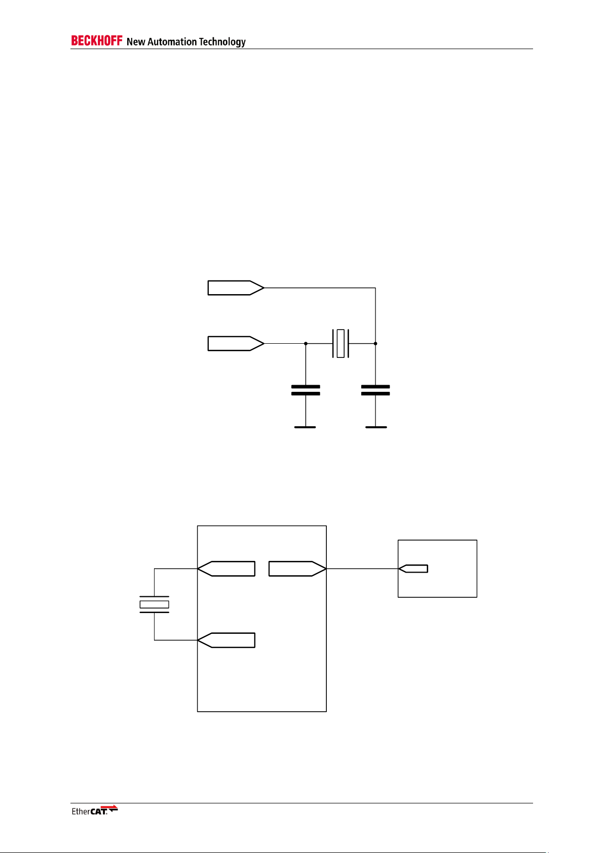
Example Schematics
OSC_IN
OSC_OUT
25 MHz
GND
PLL
GND
PLL
25 MHz
OSC_OUT
OSC_IN
ET1200
CLK25OUT
Ethernet
PHY
CLK25
9 Example Schematics
9.1 Clock Adoption
The layout of the clock source has the biggest influence on EMC/EMI of a system design.
Although a clock frequency of 25 MHz requires not extensive design efforts, the following rules shall
help to improve system performance:
Keep clock source and ESC as close as possible close together.
Ground Layer should be seamless in this area.
Power supply should be of low impedance for clock source and ESC clock supply.
Capacitors shall be used as recommended by the clock source component.
Capacities between clock source and ESC clock supply should be in the same size (values
depend upon geometrical form of board).
The initial accuracy of the ET1200 clock source has to be 25ppm or better.
Figure 23: Quartz crystal connection
NOTE: The value of the load capacitors depends on the load capacitance of the crystal, the pin capacitance C
of the ESC pins and the board design (typical 12pF each if CL = 10pF).
Figure 24: Quartz crystal Clock source for ET1200 and Ethernet PHYs
OSC
Slave Controller – ET1200 Hardware Description III-45
Page 56
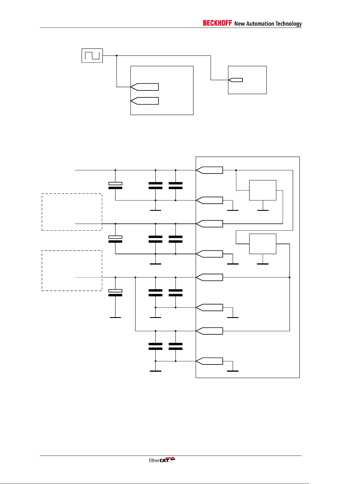
Example Schematics
25 MHz
OSC_OUT
OSC_IN
ET1200 Ethernet
PHY
CLK25
Optional external
V
CC I/O
supply
(e.g., V
CC I/O Ext
= Vcc)
Optional external core
supply
ET1200
V
CC_PLL
V
CC Core
V
CC I/O
V
CC I/O Ext
GND
PLL
GND
Core
GND
I/O
GND
PLL
GND
Core
GND
I/O
LDO
Vcc Core
V
CC Core Ext
V
CC
V
CC
GND
LDO
Vcc I/O
GND
GND
Core
220pF100 nF
10µF
220pF100 nF
10µF
220pF100 nF
10µF
220pF100 nF
Figure 25: Oscillator clock source for ET1200 and Ethernet PHYs
9.2 Power supply
Recommendation for voltage stabilization capacitors: 220pF and 100nF ceramic capacitors for each power pin
pair, additional 10µF tantalum electrolytic capacitor for VCC, V
capacitors.
GND, GND
The internal LDOs are self-deactivating if the actual V
respective nominal LDO output voltage.
III-46 Slave Controller – ET1200 Hardware Description
I/O
, GND
, and GND
Core
Figure 26: ET1200 power supply
can be connected to a single GND potential.
PLL
CC I/O
CCI/O
, and V
or VCC
CC Core/VCC PLL
Core/VCC PLL
, i.e., a total of three 10µF
voltage is higher than the
Page 57
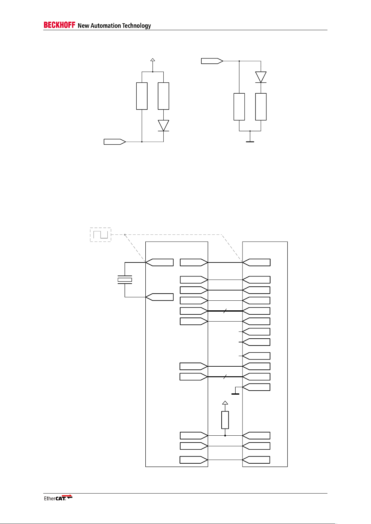
Example Schematics
V
CC I/O
4K7
Pull-Up Pull-Down
Pin
Pin
4K7
25 MHz
OSC_OUT
OSC_IN
ET1200
CLK25OUT
Ethernet PHY
RX_DV
RX_DATA[3:0]
RX_ERR
TX_ENA
TX_DATA[3:0]
RX_CLK
RX_DV
RXD[3:0]
RX_ER
TX_EN
TXD[3:0]
RX_CLK
TX_CLK
CLK25
CRS
TX_ER
COL
LINK_MII
LINK_STATUS
25 MHz
Option: one quartz oscillator for
ET1200 and PHY
!
!
!
MI_DATA
MI_CLK
MDIO
MDC
4K7
V
CC I/O
RESET RESET
9.3 Dual purpose configuration input/LED output pins
Figure 27: Dual purpose configuration input/LED output pins
9.4 PHY Connection
Refer to chapter 3.7.1 for more information on special markings (!). Take care of proper configuration
of TX Shift and PHY addresses.
Figure 28: PHY Connection
Slave Controller – ET1200 Hardware Description III-47
Page 58

Example Schematics
EBUS_RX-
EBUS_RX+
R
L
=100R
ET1200
R
LI+
R
LI-
V
CC I/O
11K
RBIAS
ET1200
Logic
Core
RESET
WPU
ET1200
V
CC I/O
Reset Other
Reset ET1200
Reset
Controller
Reset
ECAT Reset
Reg. 0x0040
Reset In
Reset Out
Optional
Optional
Power
Supervisor
V
CC I/OVCC Core
GND
I/O
R
V
CC I/O
9.5 LVDS termination
The LVDS termination with an impedance of 100 Ω is typically achieved by a resistor R
only necessary for EBUS ports and should be placed adjacent to the EBUS_RX inputs.
Figure 29: LVDS termination
9.6 RBIAS resistor
The LVDS RBIAS resistor should have a value of R
=11 kΩ.
BIAS
=100 Ω. It is
L
Figure 30: RBIAS resistor
9.7 Reset Logic
Figure 31: Reset Logic
III-48 Slave Controller – ET1200 Hardware Description
Page 59

Electrical Specifications and Timings
Symbol
Parameter
Condition
Min
Max
Units
VCC-VSS
Supply voltage for
internal LDO
-0.3
5.5
V
I
CC
Supply current
Internal LDOs used for V
CC I/O
and
V
CC Core
110
mA
I
CC I/O
Supply current
V
CC I/O
sourced externally, LDO
used for V
CC Core
60
mA
I
CC Core
Supply current
V
CC I/O
and V
CC Core
sourced
externally
100
mA
V
ESC
ESD protection
Human body model, according to
MIL-STD-883E-3015.7 Class 1
2 kV
I
DC_ESD
Permanent current into
ESD protection diodes
Only in case of forward biased
ESD diodes. Input voltage above
V
CCI/O
or below V
SS
2 mA
Symbol
Parameter
Min
Typ
Max
Units
VCC
Power supply
3.0
5.0
5.5
V
V
CC I/O
I/O power supply
3.0
3.3
5.5
V
V
CC Core
Logic power supply
2.25
2.5
2.75
V
V
CC PLL
PLL power supply
2.25
2.5
2.75
V
V
CC I/O Ext
External I/O power supply
3.3
3.3
5.5
V
V
CC Core Ext
External logic power supply
2.5
2.5
2.75
V
V
CC PLL Ext
External PLL power supply
2.5
2.5
2.75
V
A
Ambient temperature
-40 85
°C
10 Electrical Specifications and Timings
10.1 Absolute Maximum Ratings
Table 48: Absolute Maximum Ratings
NOTE: Supply current does not include output driver current for PDIs and LEDs.
10.2 Electrical Characteristics
Table 49: Operating Conditions
Slave Controller – ET1200 Hardware Description III-49
Page 60

Electrical Specifications and Timings
Symbol
Parameter
Condition
Min
Typ
Max
Units
V
CC I/O LDO
Internal LDO output voltage
V
CC I/O
3.2 V
V
CC Core LDO
Internal LDO output voltage
V
CC Core/VCC PLL
2.4 V
V
Reset I/O
Reset threshold for V
CC I/O
2.8 V
V
Reset Core
Reset threshold for V
CC Core
1.6 V
V
IL
Input Low voltage (not OSC_IN)
0.7
V
V
IH
Input High voltage (not OSC_IN)
a) V
CC I/O
=3.3V
b) V
CC I/O
=5V
2.0
a) 3.6
b) 5.5
V
V
IT OSC_IN
Input threshold voltage OSC_IN
(no Schmitt trigger)
a) V
CC I/O
=3.3V
b) V
CC I/O
=5V
a) 1.4
b) 2.2
a) 1.6
b) 2.5
a) 1.8
b) 2.8
V
V
OL
Output Low voltage
0.4
V
V
OH
Output High voltage
2.4
V
V
OD
LVDS differential output voltage
RL=100 Ω
R
BIAS
=11 kΩ
245
350
455
mV
ΔV
OD
Change in VOD between 1 and 0
±50
mV
VOC
LVSDS common mode output
voltage
1.125
1.25
1.375
V
ΔV
OC
Change in VOC between 1 and 0
±50
mV
V
ID
LVDS differential input voltage
100
mV
VIC
LVDS input voltage range
0
2.4
V
I
OH
Output High current
4
mA
I
OL
Output Low current
-3
mA
I
IL
Input leakage current (without
internal PU/PD)
±10
µA
I
OL
Output leakage current (tristate,
without internal PU/PD)
±10
µA
R
PU
Internal pull-up resistor
1.6
3.3 7 kΩ
R
WPU
Weak internal pull-up resistor
a) V
CC I/O
=3.3V
b) V
CC I/O
=5V
a) 75
b) 50
a) 110
b) 70
a) 190
b) 120
kΩ
R
WPD
Weak internal pull-down resistor
a) V
CC I/O
=3.3V
b) V
CC I/O
=5V
a) 60
b) 40
a) 95
b) 60
a) 180
b) 110
kΩ
R
LI+
Internal LVDS input pull-down
resistor at EBUS_RX+ pins
15
27
45
kΩ
R
LI-
Internal LVDS input pull-up
resistor at EBUS_RX- pins
15
27
45
kΩ
R
BIAS
External LVDS BIAS resistor
11 kΩ
RL
LVDS RX load resistor
100 Ω
C
OSC
OSC_IN/OSC_OUT pin
capacitance
1.2 pF
Table 50: DC Characteristics
NOTE: R
transistors).
NOTE: Input and output characteristics without special indication apply to all non-LVDS I/O signals.
WPU/RWPD
III-50 Slave Controller – ET1200 Hardware Description
cannot be used externally, their full effectiveness appears only inside the ET1200 (realized as
Page 61

Electrical Specifications and Timings
Configuration
External supply voltage
Supply current (typical)
VCC
V
CC I/O
V
CC Core
ICC
I
CC I/O
I
CC Core
2 EBUS ports
3.3V
3.3V
Int. LDO
70 mA
17 mA - 5V
Int. LDO
Int. LDO
87 mA - -
5V
5V
Int. LDO
72 mA
36 mA
-
3.3V
3.3V
2.5V
1 mA
17 mA
75 mA
5V
Int. LDO
2.5V
16 mA
-
75 mA
5V
5V
2.5V
1 mA
40 mA
75 mA
3 EBUS ports
3.3V
3.3V
Int. LDO
74 mA
24 mA - 5V
Int. LDO
Int. LDO
97 mA - -
5V
5V
Int. LDO
76 mA
43 mA
-
3.3V
3.3V
2.5V
1 mA
24 mA
79 mA
5V
Int. LDO
2.5V
23 mA
-
79 mA
5V
5V
2.5V
1 mA
43 mA
79 mA
1 EBUS port, 1 MII
port
3.3V
3.3V
Int. LDO
68 mA
10 mA - 5V
Int. LDO
Int. LDO
78 mA - -
5V
5V
Int. LDO
69 mA
25 mA
-
3.3V
3.3V
2.5V
1 mA
10 mA
72 mA
5V
Int. LDO
2.5V
10 mA
-
72 mA
5V
5V
2.5V
1 mA
26 mA
72 mA
2 EBUS ports, 1 MII
port
3.3V
3.3V
Int. LDO
71 mA
18 mA - 5V
Int. LDO
Int. LDO
89 mA - -
5V
5V
Int. LDO
73 mA
34 mA
-
3.3V
3.3V
2.5V
1 mA
18 mA
76 mA
5V
Int. LDO
2.5V
17 mA
-
76 mA
5V
5V
2.5V
1 mA
37 mA
76 mA
Table 51: DC Characteristics (Supply current)
NOTE: Int. LDO means internal LDO is used, otherwise power is supplied externally. Supply current does not
include output driver current for PDIs and LEDs.
Slave Controller – ET1200 Hardware Description III-51
Page 62

Electrical Specifications and Timings
Symbol
Parameter
Min
Typ
Max
Units
f
CLK25
Clock source (OSC_IN) with initial accuracy
25 MHz ± 25 ppm
t
CLK25OUT
CLK25OUT rising edge after OSC_IN rising
edge
22 ns
t
TX_delay
TX_ENA/TX_D[3:0] edge (TX-Shift = 00) after
rising edge of
a) OSC_IN
b) CLK25OUT
a) 4
b) 22
ns
t
CPU_CLK
CPU_CLK (25 MHz) rising edge after OSC_IN
rising edge
4
t
POR_Sample
POR value sample time after power good
84
ms
t
Driver_Enable
Output drivers enabled after POR values
sampled (not PDI and not Sync/LatchSignals)
80 ns
t
Reset_In
External reset input time
50
ns
t
Reset_Out
ET1200 Reset output time
80
84
ms
t
Reset_Func
ET1200 functional after RESET signal high
(EEPROM not loaded, PDI not functional)
50
µs
t
Startup
Startup time (PDI operational after power
good, without SII loading error)
340
ms
Table 52: AC Characteristics
The AC characteristics of the PDIs, Distributed Clocks, SII EEPROM I2C interface, and MII interface
can be found in their respective chapters.
III-52 Slave Controller – ET1200 Hardware Description
Page 63

Electrical Specifications and Timings
V
CC I/O
/V
CC Core
Power good
t
POR_Sample
ET1200 reset controller
output (Reset Out)
Functional reset
(ET1200 logic core)
RESET pin
t
Reset_Out
t
Reset_Func
t
Reset_Out
t
Reset_Func
t
Reset_Func
t
Reset_In
External reset source
ECAT Reset initiated
Reset threshold
Power-On Reset External Reset ECAT Reset (Reg. 0x0040)
Power-On values sampled
t
Driver_Enable
Output drivers enabled
(not PDI and not Sync/Latch)
Figure
32: Reset Timing
ional at Power
-good time. Otherwise t
POR_Sampe
is delayed.
Slave Controller – ET1200 Hardware Description III-53
Page 64
Electrical Specifications and Timings
Symbol
Parameter
Min
Average
Max
Units
t
Diff
Average difference processing delay minus
forwarding delay (without RX FIFO jitter)
between any two ports
20
ns
t
EE
EBUS port to EBUS port delay (FIFO size 7):
a) Through ECAT Processing Unit
(processing), Low Jitter off
b) Alongside ECAT Processing Unit
(forwarding), Low Jitter off
c) Through ECAT Processing Unit
(processing), Low Jitter on
d) Alongside ECAT Processing Unit
(forwarding), Low Jitter on
a) 140
b) 120
c) 150
d) 130
a) 150
b) 130
c) 155
d) 135
a) 160
b) 140
c) 160
d) 140
ns
t
EM
EBUS port to MII port delay (FIFO size 7):
a) Through ECAT Processing Unit
(processing)
b) Alongside ECAT Processing Unit
(forwarding)
a) 145
b) 125
a) 170
b) 150
a) 195
b) 175
ns
t
ME
MII port to EBUS port delay (FIFO size 7):
a) Through ECAT Processing Unit
(processing), Low Jitter off
b) Alongside ECAT Processing Unit
(forwarding), Low Jitter off
c) Through ECAT Processing Unit
(processing), Low Jitter on
d) Alongside ECAT Processing Unit
(forwarding), Low Jitter on
a) 255
b) 235
c) 265
d) 245
a) 280
b) 260
c) 290
d) 270
a) 305
b) 285
c) 315
d) 295
ns
t
MM
MII port to MII port delay
(FIFO size 7, TX Shift=00):
Through ECAT Processing Unit (processing)
280
305
335
ns
Table 53: Forwarding Delays
NOTE: Average timings are used for DC calculations.
III-54 Slave Controller – ET1200 Hardware Description
Page 65
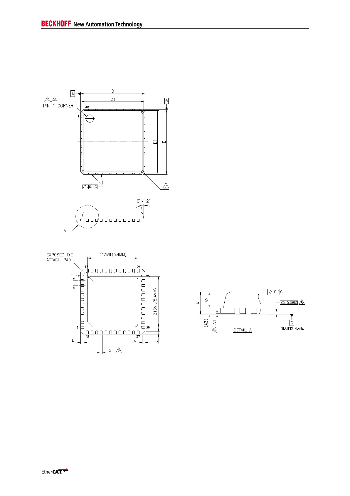
Mechanical Specifications
11 Mechanical Specifications
11.1 Package Information
A 48 pin QFN package is used for the ET1200. The ET1200 is RoHS compliant. The plating material
of the leads is 100% Sn.
Figure 33: Package Outline
Slave Controller – ET1200 Hardware Description III-55
Page 66
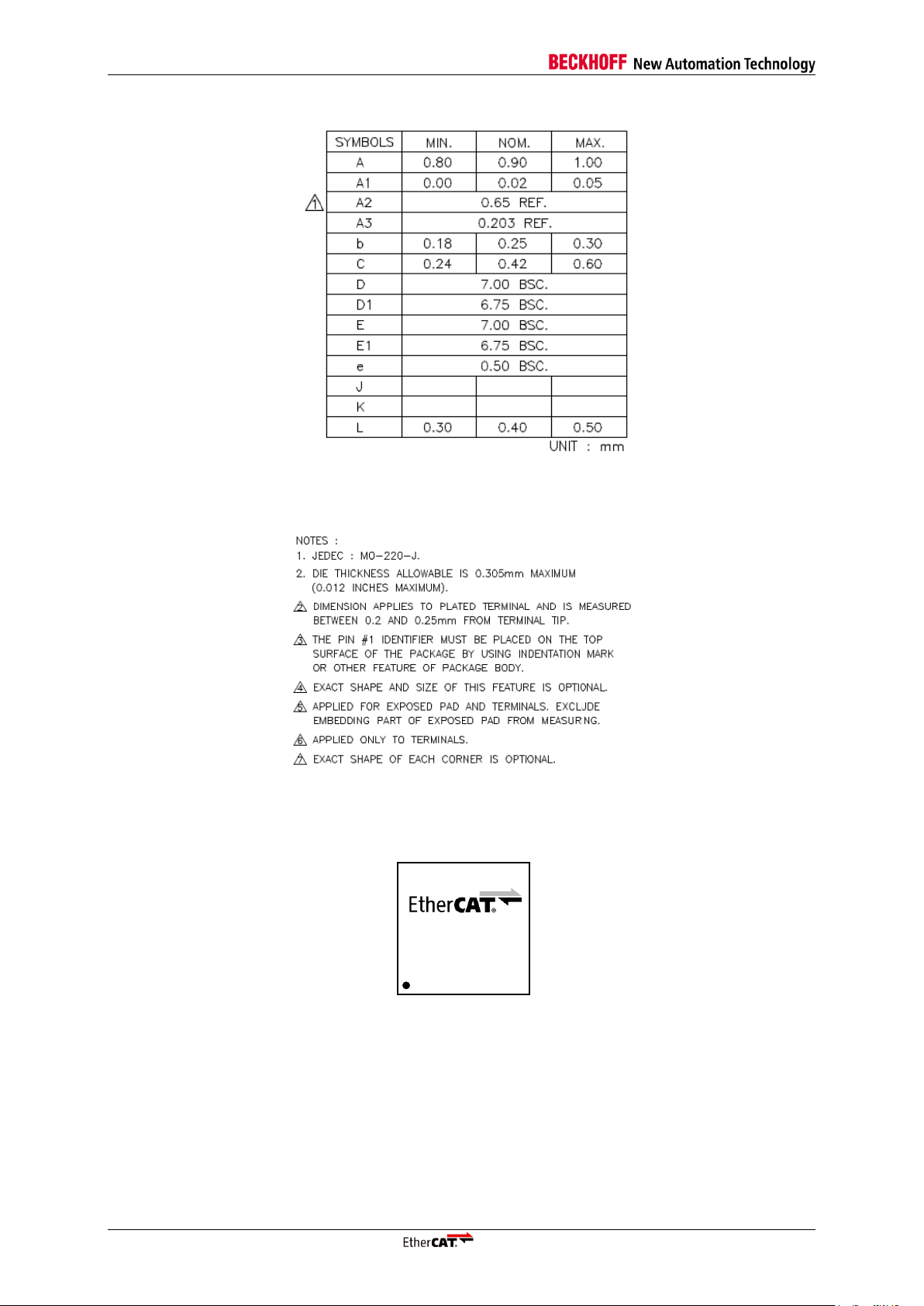
Mechanical Specifications
BECKHOFF ET1200
YYWW 000X
LLLLLL.LL
Figure 34: Dimensions
Figure 35: Notes
The chip label contains the date code (X=stepping, YY=year, WW=week, optional: LLL…= lot ID).
Figure 36: Chip Label
III-56 Slave Controller – ET1200 Hardware Description
Page 67
Mechanical Specifications
Symbol
Parameter
Min
Max
Units
Storage
Storage temperature
-65
150
°C
11.2 Moisture Sensitivity and Storage
The ET1200 is shipped in a sealed moisture barrier bag (dry-pack). There is a “caution” label on the
dry-pack which contains all necessary information required for handling the devices. Refer to the
JEDEC standards J-STD-020 and J-STD-033 for more details (http://www.jedec.org).
The information on the dry-pack takes precedence over information in this chapter.
The moisture sensitivity level of the ET1200 is MSL 3. The maximum shelf-life of the ET1200 packed
in a dry-pack is one year after bag seal date. If the ET1200 is stored longer than one year, drying
(baking) is required before soldering.
Drying and re-packaging can have negative effects on solderability and conducting surfaces. To
minimize issues, the following steps should be taken:
Visual inspection of the ET1200 devices
solderability tests with some samples of the ET1200
final test of the product using the ET1200 with focus on the ET1200 connections
Table 54: Absolute Maximum Storage Conditions
Slave Controller – ET1200 Hardware Description III-57
Page 68
Mechanical Specifications
260°C
218°C
200°C
150°C
25°C
255°C
60-120 s
max. 8 min.
60-120 s
Preheating Soldering Cooling
ramp up: max. 3°C/s
ramp down: max. 6°C/s
max. 12 s
Time
Temperature
Liquidus
L
L
11.3 Soldering Profile
The following soldering profile is a maximum soldering profile. For the actual soldering profile many
factors have to be taken into consideration, e.g., solder paste characteristics, the PCB, other
components, materials, and process type. An example soldering profile is shown below.
Figure 37: Maximum Soldering Profile
Figure 38: Example Soldering Profiles
III-58 Slave Controller – ET1200 Hardware Description
Page 69

Mechanical Specifications
Symbol
Parameter
Example
Abs. Max.
Units
L
Liquidus temperature
218
°C
t
L
Time above
L
(TAL)
45
s
P
Peak temperature
240
260
°C
t
P
Time at
P
10
12
s
NR
Number of reflow cycles
1
3
Table 55: Example Soldering Profile
11.4 Ordering codes
The ordering codes for the ET1200 devices are composed like this:
ET1200-0000-NNNN
The code part NNNN identifies the size of the packing unit. Do not confuse the ordering codes with the
stepping code ET1200-0000. You will always get the latest stepping while the ordering codes are
unchanged.
Slave Controller – ET1200 Hardware Description III-59
Page 70

Appendix
12 Appendix
12.1 Support and Service
Beckhoff and our partners around the world offer comprehensive support and service, making
available fast and competent assistance with all questions related to Beckhoff products and system
solutions.
12.1.1 Beckhoff’s branch offices and representatives
Please contact your Beckhoff branch office or representative for local support and service on Beckhoff
products!
The addresses of Beckhoff's branch offices and representatives round the world can be found on her
internet pages: http://www.beckhoff.com
You will also find further documentation for Beckhoff components there.
12.2 Beckhoff Headquarters
Beckhoff Automation GmbH
Eiserstr. 5
33415 Verl
Germany
Phone: +49 (0) 5246 963-0
Fax: +49 (0) 5246 963-198
E-mail: info@beckhoff.com
Web: www.beckhoff.com
Beckhoff Support
Support offers you comprehensive technical assistance, helping you not only with the application of
individual Beckhoff products, but also with other, wide-ranging services:
world-wide support
design, programming and commissioning of complex automation systems
and extensive training program for Beckhoff system components
Hotline: +49 (0) 5246 963-157
Fax: +49 (0) 5246 963-9157
E-mail: support@beckhoff.com
Beckhoff Service
The Beckhoff Service Center supports you in all matters of after-sales service:
on-site service
repair service
spare parts service
hotline service
Hotline: +49 (0) 5246 963-460
Fax: +49 (0) 5246 963-479
E-mail: service@beckhoff.com
III-60 Slave Controller – ET1200 Hardware Description
 Loading...