

Page 1

Documentation | EN
EPP4374-0002
EtherCAT P Box with analog inputs and outputs
2020-09-22 | Version: 1.1
Page 2

Page 3

Table of contents
Table of contents
1 Foreword ....................................................................................................................................................5
1.1 Safety instructions .............................................................................................................................5
1.2 Notes on the documentation..............................................................................................................6
1.3 Documentation issue status ..............................................................................................................7
2 Product group: EtherCATP Box modules ..............................................................................................8
3 Product overview.......................................................................................................................................9
3.1 Introduction........................................................................................................................................9
3.2 Technical data .................................................................................................................................10
3.3 Scope of supply ...............................................................................................................................12
3.4 Process image.................................................................................................................................13
4 Mounting and cabling..............................................................................................................................15
4.1 Mounting..........................................................................................................................................15
4.1.1 Dimensions ...................................................................................................................... 15
4.1.2 Fixing ............................................................................................................................... 16
4.1.3 Functional earth (FE) ....................................................................................................... 16
4.1.4 Tightening torques for plug connectors ........................................................................... 16
4.2 Cabling ............................................................................................................................................17
4.2.1 EtherCATP...................................................................................................................... 18
4.2.2 Analog interfaces ............................................................................................................. 21
4.3 UL Requirements.............................................................................................................................24
5 Commissioning and configuration ........................................................................................................25
5.1 Integration in TwinCAT ....................................................................................................................25
5.2 Parameterizing signal ranges ..........................................................................................................26
5.3 Object overview ...............................................................................................................................27
5.4 Object description and parameterization .........................................................................................33
5.4.1 Objects to be parameterized during commissioning........................................................ 33
5.4.2 Standard objects (0x1000-0x1FFF) ................................................................................. 38
5.4.3 Profile-specific objects (0x6000-0xFFFF) ........................................................................ 43
5.5 Restoring the delivery state .............................................................................................................46
6 Appendix ..................................................................................................................................................47
6.1 General operating conditions...........................................................................................................47
6.2 Accessories .....................................................................................................................................48
6.3 Version identification of EtherCAT devices .....................................................................................49
6.3.1 Beckhoff Identification Code (BIC)................................................................................... 53
6.4 Support and Service ........................................................................................................................55
EPP4374-0002 3Version: 1.1
Page 4

Table of contents
EPP4374-00024 Version: 1.1
Page 5
Foreword
1 Foreword
1.1 Safety instructions
Safety regulations
Please note the following safety instructions and explanations!
Product-specific safety instructions can be found on following pages or in the areas mounting, wiring,
commissioning etc.
Exclusion of liability
All the components are supplied in particular hardware and software configurations appropriate for the
application. Modifications to hardware or software configurations other than those described in the
documentation are not permitted, and nullify the liability of Beckhoff Automation GmbH & Co. KG.
Personnel qualification
This description is only intended for trained specialists in control, automation and drive engineering who are
familiar with the applicable national standards.
Description of instructions
In this documentation the following instructions are used.
These instructions must be read carefully and followed without fail!
DANGER
Serious risk of injury!
Failure to follow this safety instruction directly endangers the life and health of persons.
WARNING
Risk of injury!
Failure to follow this safety instruction endangers the life and health of persons.
CAUTION
Personal injuries!
Failure to follow this safety instruction can lead to injuries to persons.
NOTE
Damage to environment/equipment or data loss
Failure to follow this instruction can lead to environmental damage, equipment damage or data loss.
Tip or pointer
This symbol indicates information that contributes to better understanding.
EPP4374-0002 5Version: 1.1
Page 6

Foreword
1.2 Notes on the documentation
Intended audience
This description is only intended for the use of trained specialists in control and automation engineering who
are familiar with the applicable national standards.
It is essential that the documentation and the following notes and explanations are followed when installing
and commissioning these components.
It is the duty of the technical personnel to use the documentation published at the respective time of each
installation and commissioning.
The responsible staff must ensure that the application or use of the products described satisfy all the
requirements for safety, including all the relevant laws, regulations, guidelines and standards.
Disclaimer
The documentation has been prepared with care. The products described are, however, constantly under
development.
We reserve the right to revise and change the documentation at any time and without prior announcement.
No claims for the modification of products that have already been supplied may be made on the basis of the
data, diagrams and descriptions in this documentation.
Trademarks
Beckhoff®, TwinCAT®, EtherCAT®, EtherCATG®, EtherCATG10®, EtherCATP®, SafetyoverEtherCAT®,
TwinSAFE®, XFC®, XTS® and XPlanar® are registered trademarks of and licensed by Beckhoff Automation
GmbH. Other designations used in this publication may be trademarks whose use by third parties for their
own purposes could violate the rights of the owners.
Patent Pending
The EtherCAT Technology is covered, including but not limited to the following patent applications and
patents: EP1590927, EP1789857, EP1456722, EP2137893, DE102015105702 with corresponding
applications or registrations in various other countries.
EtherCAT® is registered trademark and patented technology, licensed by Beckhoff Automation GmbH,
Germany.
Copyright
© Beckhoff Automation GmbH & Co. KG, Germany.
The reproduction, distribution and utilization of this document as well as the communication of its contents to
others without express authorization are prohibited.
Offenders will be held liable for the payment of damages. All rights reserved in the event of the grant of a
patent, utility model or design.
EPP4374-00026 Version: 1.1
Page 7

Foreword
1.3 Documentation issue status
Version Comment
1.1 • Front page updated
• Structure update
1.0 • First release
0.1 • First preliminary version
Firmware and hardware versions
This documentation refers to the firmware and hardware version that was applicable at the time the
documentation was written.
The module features are continuously improved and developed further. Modules having earlier production
statuses cannot have the same properties as modules with the latest status. However, existing properties
are retained and are not changed, so that older modules can always be replaced with new ones.
Documentation Firmware Hardware
1.1 04 03
1.0 04 03
The firmware and hardware version (delivery state) can be found in the batch number (D-number) printed on
the side of the EtherCAT Box.
Syntax of the batch number (D-number)
D: WW YY FF HH
WW - week of production (calendar week)
YY - year of production
FF - firmware version
HH - hardware version
Further information on this topic: Version identification of EtherCAT devices [}49].
Example with D no. 29 10 02 01:
29 - week of production 29
10 - year of production 2010
02 - firmware version 02
01 - hardware version 01
EPP4374-0002 7Version: 1.1
Page 8
Product group: EtherCATP Box modules
2 Product group: EtherCATP Box modules
EtherCATP
EtherCATP supplements the EtherCAT technology with a process in which communication and supply
voltages are transmitted on a common line. All EtherCAT properties are retained with this process.
Two supply voltages are transmitted per EtherCATP line. The supply voltages are electrically isolated from
each other and can therefore be switched individually. The nominal supply voltage for both is 24 VDC.
EtherCAT P uses the same cable structure as EtherCAT: a 4-core Ethernet cable with M8 connectors. The
connectors are mechanically coded so that EtherCAT connectors and EtherCATP connectors cannot be
interchanged.
EtherCATP Box modules
EtherCATP Box modules are EtherCATP slaves with IP67 protection. They are designed for operation in
wet, dirty or dusty industrial environments.
Fig.1: EtherCATP
EtherCAT basics
A detailed description of the EtherCAT system can be found in the EtherCAT system documentation.
EPP4374-00028 Version: 1.1
Page 9
3 Product overview
3.1 Introduction
Product overview
Fig.2: EPP4374-0002
EtherCAT Box with analog inputs and outputs
EPP4374-0002 has two analog inputs and two analog outputs. The signal range can be individually
parameterized for each analog input and output:
• -10 .. +10V
• 0 .. 10V
• 0 .. 20mA
• 4 .. 20mA
Quick links
Technical data [}10]
Process image [}13]
Signal connection [}21]
EPP4374-0002 9Version: 1.1
Page 10

Product overview
3.2 Technical data
All values are typical values over the entire temperature range, unless stated otherwise.
Technical data EPP4374-0002
Fieldbus
Fieldbus EtherCAT
Connection EtherCAT P: Combined connection for EtherCAT and supply
voltages
Input: 1 x M8 socket, 4-pin, P-coded
Downstream connection: 1 x M8 socket, 4-pin, P-coded
Supply voltages
Connection See Fieldbus connection
Control voltage U
Nominal voltage 24VDC (-15%/ +20%)
Sum current max. 3A
Consumers Module electronics: 120mA at 24V
Peripheral voltage U
Nominal voltage 24VDC (-15%/ +20%)
Sum current max. 3A
Consumers • Sensors
Analog inputs
Number 2
Connection M12 socket, 5-pin connection
Signal range Parameterizable:
Electrical specifications [}11]
Sensor/actuator
supply voltage
Analog outputs
Number 2
Connection M12 socket, 5-pin connection
Output signal range Parameterizable:
Electrical specifications [}11]
Sensor/actuator
supply voltage
S
1)
DC
P
1)
2)
• Actuators
2)
• -10 .. +10V (default)
• 0 .. 10V
• 0 .. 20mA
• 4 .. 20mA
3)
from the peripheral voltage U
P
max. 3A in total, not short-circuit proof
• -10 .. +10V (default)
• 0 .. 10V
• 0 .. 20mA
• 4 .. 20mA
3)
from the peripheral voltage U
P
max. 3A in total, not short-circuit proof
1)
Sum current of consumers and power transmission.
2)
"Actuators": Field devices that are intended to be connected to outputs.
"Sensors": Field devices that are intended to be connected to inputs.
3)
Supply voltage that is available on the plug connectors of the analog interfaces.
EPP4374-000210 Version: 1.1
Page 11

Product overview
Technical data EPP4374-0002
Environmental conditions
Ambient temperature during operation -25…+60°C
-25…+55°C according to cURus [}24]
0…+55°C according to ATEX
Ambient temperature during storage -40…+85°C
Vibration/ shock resistance conforms to EN 60068-2-6 / EN 60068-2-27;
see also Additional checks [}12].
EMC immunity/emission conforms to EN61000-6-2/ EN61000-6-4
Protection class IP65, IP66, IP67 conforms to EN60529
Mechanics
Weight approx. 165g
Installation position variable
Approvals and conformity
Approvals
Analog inputs
The signal range can be switched during operation. The following table shows the electrical specifications
depending on the selected signal range.
CE, cURus [}24]
Technical data Signal range
-10 .. 10V 0 .. 10V 0 .. 20mA 4 .. 20mA
Input type Differential
Input resistance >200kΩ >200kΩ 85Ω typ. + diode
voltage
Digital resolution 16-bit 15-bit 15-bit 15-bit
Measuring error < 0.3% relative to full scale value
Conversion time approx. 100µs
Input filter limit frequency 5kHz
Value of the least significant
bit
The analog inputs and outputs have a common analog ground potential. The analog ground potential is
electrically isolated from all other ground potentials in the box.
Analog outputs
The output signal range can be switched during operation. The following table shows the electrical
specifications depending on the selected output signal range.
Technical data Output signal range
Load resistor / load >5kΩ >5kΩ <500Ω <500Ω
Digital resolution 16-bit 15-bit 15-bit 15-bit
Output error < 0.1 % (ambient temperature 0 °C ... +55 °C)
Conversion time approx. 40µs
Value of the least significant
bit
approx. 305µV approx. 305µV approx. 610µA approx. 488µA
-10 .. 10V 0 .. 10V 0 .. 20mA 4 .. 20mA
< 0.2 % (ambient temperature < 0 °C or > 55 °C)
related to the final value.
approx. 305µV approx. 305µV approx. 610µA approx. 488µA
85Ω typ. + diode
voltage
The analog inputs and outputs have a common analog ground potential. The analog ground potential is
electrically isolated from all other ground potentials in the box.
EPP4374-0002 11Version: 1.1
Page 12

Product overview
Additional checks
The boxes have been subjected to the following checks:
Verification Explanation
Vibration 10 frequency sweeps in 3 axes
5Hz<f<60Hz displacement 0.35mm, constant amplitude
60.1Hz<f<500Hz acceleration 5g, constant amplitude
Shocks 1000 shocks in each direction, in 3 axes
35g, 11ms
3.3 Scope of supply
Make sure that the following components are included in the scope of delivery:
• 1x EtherCAT P Box EPP4374-0002
• 2x protective cap for EtherCATP socket, M8, red (pre-assembled)
• 10x labels, blank (1 strip of 10)
Pre-assembled protective caps do not ensure IP67 protection
Protective caps are pre-assembled at the factory to protect connectors during transport. They may
not be tight enough to ensure IP67 protection.
Ensure that the protective caps are correctly seated to ensure IP67 protection.
EPP4374-000212 Version: 1.1
Page 13
3.4 Process image
3.4.1 Assignment of connectors to process data objects
Process image in TwinCAT Connector Process data object
X01
AI Inputs Channel1
Product overview
X02
X03
X04
AI Inputs Channel2
AO Outputs Channel 3
AO Outputs Channel 4
3.4.2 Content of the process data objects
AI Inputs Channel1
The data for the first analog channel can be found under AI Inputs Channel1.
• Underrange: Value of the analog input is less than 0/4mA or -10/0V
• Overrange: Value of the analog input is greater than 20mA or +10V
• Limit1: with activated limit 1 (object 0x80x0:07 [}35]= 1) means
1: value less than limit 1 (set in object 0x80x0:13 [}35])
2: value greater than limit 1 (set in object 0x80x0:13 [}35])
3: value equal to limit 1 (set in object 0x80x0:13 [}35])
• Limit2: with activated limit 2 (object 0x80x0:08 [}35]= 1) means
1: value less than limit 2 (set in object 0x80x0:14 [}35])
2: value greater than limit 2 (set in object 0x80x0:14 [}35])
3: value equal to limit 2 (set in object 0x80x0:14 [}35])
• Error: This bit is set if overrange or underrange was detected.
EPP4374-0002 13Version: 1.1
Page 14

Product overview
AI Inputs Channel2
The data of the second analog channelhave the same structure as those of the first channel.
AO Outputs Channel3
The data for the third analog channel can be found under AO Outputs Channel3.
AO Outputs Channel4
The data of the forth analog channelhave the same structure as those of the third channel.
EPP4374-000214 Version: 1.1
Page 15
4 Mounting and cabling
119
126
23
3026.5
14
Ø 3.5
13.5
4.1 Mounting
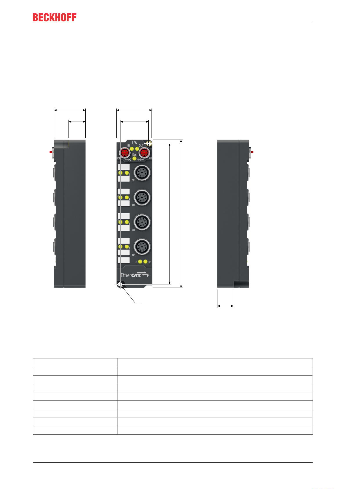
4.1.1 Dimensions
Mounting and cabling
Fig.3: Dimensions
All dimensions are given in millimeters.
Housing features
Housing material PA6 (polyamide)
Sealing compound polyurethane
Mounting two fastening holes Ø 3.5 mm for M3
Metal parts brass, nickel-plated
Contacts CuZn, gold-plated
Installation position variable
Protection class IP65, IP66, IP67 (conforms to EN 60529) when screwed together
Dimensions (H x W x D) approx. 126 x 30 x 26.5 mm (without connectors)
Weight approx. 165g
EPP4374-0002 15Version: 1.1
Page 16
Mounting and cabling
FE
4.1.2 Fixing
NOTE
Dirt during assembly
Dirty connectors can lead to malfunctions. Protection class IP67 can only be guaranteed if all cables and
connectors are connected.
• Protect the plug connectors against dirt during the assembly.
Mount the module with two M3 screws on the fastening holes in the corners of the module. The fastening
holes have no thread.
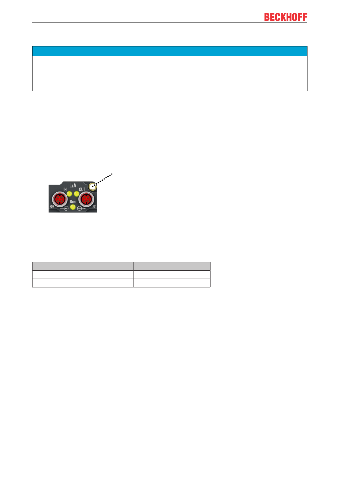
4.1.3 Functional earth (FE)
The upper fastening hole also serves as a connection for functional earth (FE).
Make sure that the box is grounded to low impedance via the functional earth (FE) connection. You can
achieve this, for example, by mounting the box on a grounded machine bed.
Fig.4: Connection for functional earth (FE)
4.1.4 Tightening torques for plug connectors
Screw connectors tight with a torque wrench. (e.g. ZB8801 from Beckhoff)
Connector diameter Tightening torque
M8 0.4Nm
M12 0.6Nm
EPP4374-000216 Version: 1.1
Page 17
Mounting and cabling
X50 X51
X01
X02
X03
X04
4.2 Cabling
Guidelines
Follow these guidelines to ensure IP67 protection:
• Mount plugs with the torque values specified below. Use a torque wrench, e.g. Beckhoff ZB8801.
• Seal unused connectors with protective caps.
• Ensure the correct seating of pre-assembled protective caps.
Protective caps are pre-assembled at the factory to protect connectors during transport. They may not
be tight enough to ensure IP67 protection.
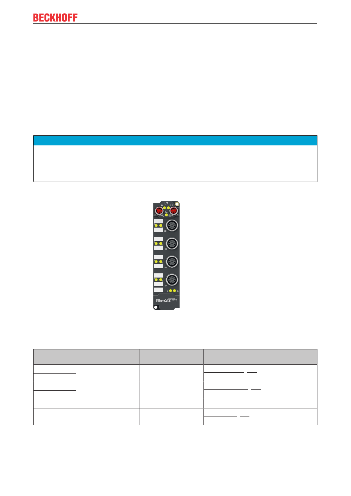
Connector overview
NOTE
Risk of confusion: Inputs and outputs
Defects possible due to mixing up of inputs and outputs. The connectors of the inputs and outputs are of
the same type.
• Observe the names of the connectors in order to avoid mistakes.
Fig.5: Connector overview
Name Connector
type
X01 M12 0.6Nm
X02
X03 M12 0.6Nm
X04
X50 M8 socket, p-coded 0.4Nm
X51 M8 socket, p-coded 0.4Nm
EPP4374-0002 17Version: 1.1
Tightening
torque
Function
Analog inputs [}21]
Analog outputs [}21]
EtherCATP [}18] input
EtherCAT P [}18] downstream
connection
Page 18
Mounting and cabling
1 2
1
2
3
4
4.2.1 EtherCATP
NOTE
Risk of damage to the device!
Bring the EtherCAT/EtherCATP system into a safe, powered down state before starting installation, disassembly or wiring of the modules!
NOTE
Pay attention to the maximum permissible current!
Pay attention also for the redirection of EtherCATP, the maximum permissible current for M8 connectors of
3A must not be exceeded!
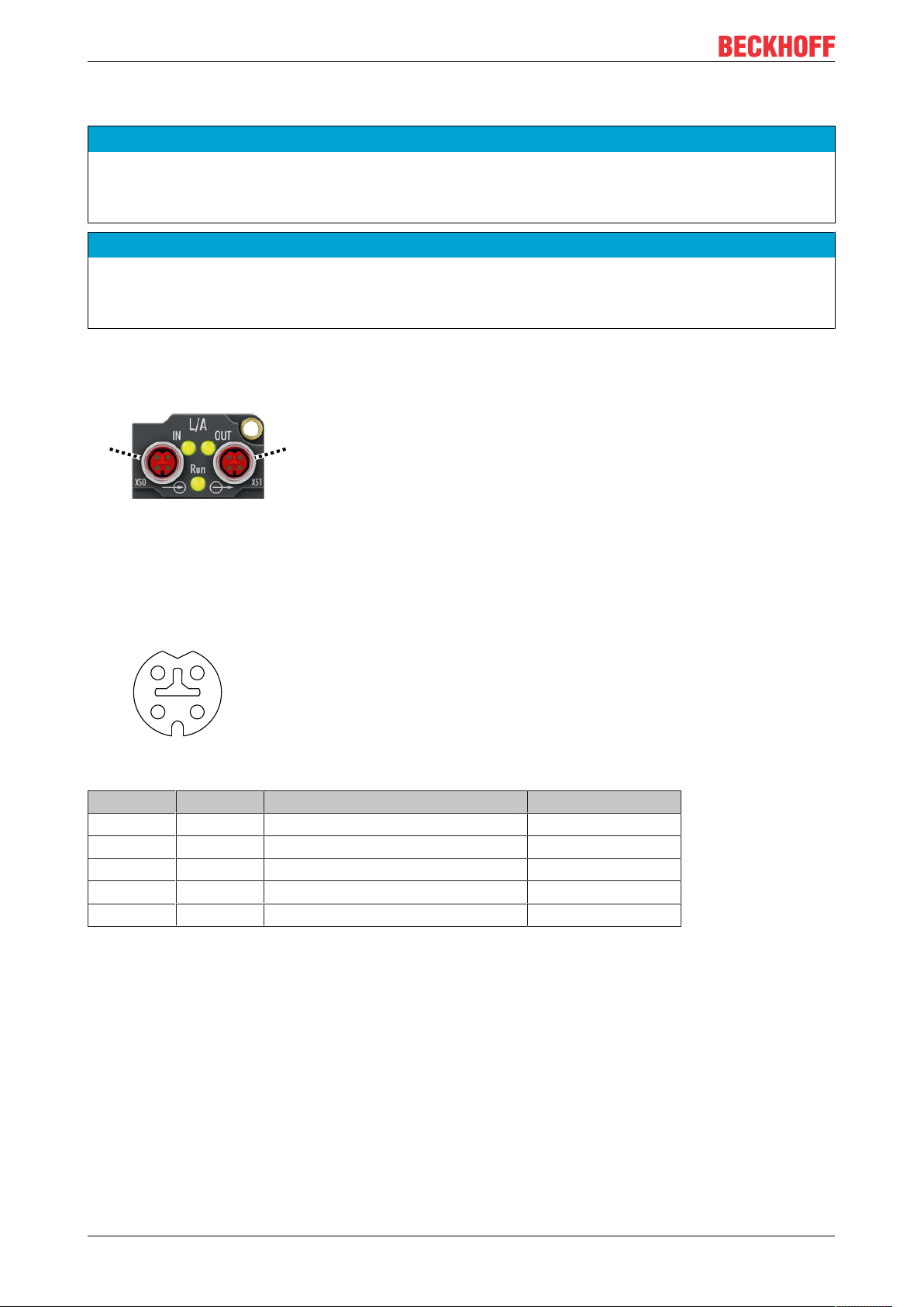
4.2.1.1 Connectors
Fig.6: Plug connectors for EtherCAT P
1 - input
2 - downstream connection
Connection
Fig.7: M8 socket, P-coded
Contact Signal Voltage Core color
1 Tx + GND
2 Rx + GND
S
P
3 Rx - UP: Peripheral voltage, +24V
4 Tx - US: Control voltage, +24V
DC
DC
yellow
white
blue
orange
Housing Shield Shield Shield
1)
The core colors apply to EtherCAT P cables and ECP cables from Beckhoff.
1)
EPP4374-000218 Version: 1.1
Page 19

Mounting and cabling
4.2.1.2 Status LEDs
4.2.1.2.1 Supply voltages
Fig.8: Status LEDs for the supply voltages
EtherCAT P Box Modules have two LEDs that display the status of the supply voltages. The status LEDs are
labelled with the designations of the supply voltages: Us and Up.
A status LED lights up green when the respective supply voltage is present.
A Status LED lights up red if the respective supply voltage is short-circuited.
4.2.1.2.2 EtherCAT
Fig.9: Status LEDs for EtherCAT
L/A (Link/Act)
A green LED labelled "L/A" or “Link/Act” is located next to each EtherCAT/EtherCATP socket. The LED
indicates the communication state of the respective socket:
LED Meaning
off no connection to the connected EtherCAT device
lit LINK: connection to the connected EtherCAT device
flashes ACT: communication with the connected EtherCAT device
Run
Each EtherCAT slave has a green LED labelled "Run". The LED signals the status of the slave in the
EtherCAT network:
LED Meaning
off Slave is in "Init" state
flashes uniformly Slave is in "Pre-Operational“ state
flashes sporadically Slave is in "Safe-Operational" state
lit Slave is in "Operational" state
Description of the EtherCAT slave states
EPP4374-0002 19Version: 1.1
Page 20

Mounting and cabling
I = 3 A
10 20
5
10
15
20
300
0
25
40
Vert. Faktor: 0,22 cm / V
Voltage drop (V)
Cable length (m)
0.14 mm²
0.22 mm²
0.34 mm²
4.2.1.3 Conductor losses
Take into account the voltage drop on the supply line when planning a system. Avoid the voltage drop being
so high that the supply voltage at the box lies below the minimum nominal voltage.
Variations in the voltage of the power supply unit must also be taken into account.
Use the planning tool for EtherCAT P in TwinCAT.
Voltage drop on the supply line
Fig.10: Voltage drop on the supply line
EPP4374-000220 Version: 1.1
Page 21

Mounting and cabling
1
2
3
4
5
4.2.2 Analog interfaces
NOTE
Signal ranges must be parameterized before carrying out the cabling
Defects possible due to incorrectly parameterized signal ranges.
• Parameterize the signal ranges [}26] before connecting the sensors and actuators.
• Parameterize the signal ranges in accordance with the specifications for the intended sensors and actuators.
NOTE
Risk of confusion: Inputs and outputs
Defects possible due to mixing up of inputs and outputs. The connectors of the inputs and outputs are of
the same type.
• Observe the names of the connectors in order to avoid mistakes.
4.2.2.1 Connectors
M12 sockets
Fig.11: M12 socket
Pin Inputs X01 and X02 Outputs X03 and X04
Symbol Description Symbol Description
1 U
P
2 In+ Analog input + U
3 GND
P
4 In- Analog input - GND
Sensor supply + Out Analog output
P
Actuator supply +
Sensor supply Ground Out GND Analog ground
P
Actuator supply Ground
5 Shield Shield
EPP4374-0002 21Version: 1.1
Page 22

Mounting and cabling
4.2.2.2 Status LEDs
Fig.12: Status LEDs at the M12 connections
Status LEDs at M12 connections 1 and 2 (inputs)
Connection LED Display Meaning
M12 socket no. 1 and 2 R
left
E
right
off No data transfer to the D/A converter
green Data transfer to the D/A converter
off Function OK
red Error: Open circuit or measured value outside of the
measuring range (smaller than 3.5mA/-11V or larger than
21mA/11V)
Correct function is indicated if the green Run LED is on and the red Error LED is off.
Status LEDs at M12 connections 3 and 4 (outputs)
Connection LED Display Meaning
M12 socket no. 3 and 4 R
left
off No data transfer to the D/A converter
green Data transfer to the D/A converter
EPP4374-000222 Version: 1.1
Page 23

Mounting and cabling
4.2.2.3 Samples
Analog inputs
Fig.13: Signal connection - Analog inputs
The sensor is connected via In+ and In-. The sensor can optionally be operated/supplied with 24VDC.
Analog outputs
Fig.14: Signal connection - Analog outputs
The actuator is connected via output+/- and outputGND. The actuator can optionally be operated/supplied
with 24VDC.
EPP4374-0002 23Version: 1.1
Page 24

Mounting and cabling
4.3 UL Requirements
The installation of the EtherCAT Box Modules certified by UL has to meet the following requirements.
Supply voltage
CAUTION
CAUTION!
This UL requirements are valid for all supply voltages of all marked EtherCAT Box Modules!
For the compliance of the UL requirements the EtherCAT Box Modules should only be supplied
• by a 24 VDC supply voltage, supplied by an isolating source and protected by means of a fuse (in accordance with UL248), rated maximum 4 Amp, or
• by a 24 VDC power source, that has to satisfy NEC class 2.
A NEC class 2 power supply shall not be connected in series or parallel with another (class 2) power
source!
CAUTION
CAUTION!
To meet the UL requirements, the EtherCAT Box Modules must not be connected to unlimited power
sources!
Networks
CAUTION
CAUTION!
To meet the UL requirements, EtherCAT Box Modules must not be connected to telecommunication networks!
Ambient temperature range
CAUTION
CAUTION!
To meet the UL requirements, EtherCAT Box Modules has to be operated only at an ambient temperature
range of 0 to 55°C!
Marking for UL
All EtherCAT Box Modules certified by UL (Underwriters Laboratories) are marked with the following label.
Fig.15: UL label
EPP4374-000224 Version: 1.1
Page 25

Commissioning and configuration
5 Commissioning and configuration
5.1 Integration in TwinCAT
The procedure for integration in TwinCAT is described in this Quick start guide.
EPP4374-0002 25Version: 1.1
Page 26

Commissioning and configuration
5.2 Parameterizing signal ranges
NOTE
Signal ranges must be parameterized before carrying out the cabling
Defects possible due to incorrectly parameterized signal ranges.
• Parameterize the signal ranges [}26] before connecting the sensors and actuators.
• Parameterize the signal ranges in accordance with the specifications for the intended sensors and actuators.
The signal range can be individually parameterized for each analog input and output. The parameters that
define the signal range are located in the CoE directory:
Interface CoE Index
Analog input X01 F800:01
Analog input X02 F800:02
Analog output X03 F800:03
Analog output X04 F800:04
TwinCAT
Proceed as follows to change the signal range of an analog channel in TwinCAT:
1. Double-click the IO module EPP4374-0002 in the IO tree.
2. Click on the "CoE - Online" tab.
ð The CoE directory is displayed.
3. Double-click on the CoE index of the interface that you wish to parameterize (see table above).
4. Select the signal range in the dialog box which then opens.
EPP4374-000226 Version: 1.1
Page 27

Commissioning and configuration
5.3 Object overview
EtherCAT XML Device Description
The display matches that of the CoE objects from the EtherCAT XML Device Description. We recommend downloading the latest XML file from the download area of the Beckhoff website and installing it according to installation instructions.
Index (hex) Name Flags Default value
1000 [}38]
1008 Device name RO EP4374-0002
1009 [}38]
100A [}38]
1011:0
[}33]
Subindex Restore default parameters RO 0x01 (1
1011:01 SubIndex 001 RW 0x00000000 (0
1018:0 Subindex Identity RO 0x04 (4
1018:01 Vendor ID RO 0x00000002 (2
1018:02 Product code RO 0x11164052 (286670930
1018:03 Revision RO 0x00110002 (1114114
1018:04 Serial number RO 0x00000000 (0
10F0:0
[}38]
1600:0
[}38]
1601:0
[}39]
1800:0
[}39]
1801:0
[}39]
1802:0
[}39]
1803:0
[}39]
1A00:0
[}39]
Subindex Backup parameter handling RO 0x01 (1
10F0:01 Checksum RO 0x00000000 (0
Subindex AO Outputs Ch.3 RO 0x01 (1
1600:01 SubIndex 001 RO 0x7020:11, 16
Subindex AO Outputs Ch.4 RO 0x01 (1
1601:01 SubIndex 001 RO 0x7030:11, 16
Subindex AI Inputs Ch.1 RO 0x06 (6
1800:06 Exclude TxPDOs RO 01 1A
Subindex AI Inputs Compact Ch.1 RO 0x06 (6
1801:06 Exclude TxPDOs RO 00 1A
Subindex AI Inputs Ch.2 RO 0x06 (6
1802:06 Exclude TxPDOs RO 03 1A
Subindex AI Inputs Compact Ch.2 RO 0x06 (6
1803:06 Exclude TxPDOs RO 02 1A
Subindex AI Inputs Ch.1 RO 0x0B (11
1A00:01 SubIndex 001 RO 0x6000:01, 1
1A00:02 SubIndex 002 RO 0x6000:02, 1
1A00:03 SubIndex 003 RO 0x6000:03, 2
1A00:04 SubIndex 004 RO 0x6000:05, 2
1A00:05 SubIndex 005 RO 0x6000:07, 1
1A00:06 SubIndex 006 RO 0x0000:00, 1
1A00:07 SubIndex 007 RO 0x0000:00, 5
1A00:08 SubIndex 008 RO 0x6000:0E, 1
1A00:09 SubIndex 009 RO 0x6000:0F, 1
1A00:0A SubIndex 010 RO 0x6000:10, 1
1A00:0B SubIndex 011 RO 0x6000:11, 16
Device type RO 0x00001389 (5001
Hardware version RO 00
Software version RO 02
)
dec
)
dec
)
dec
)
dec
)
dec
)
dec
)
dec
)
dec
)
dec
dec
)
dec
)
dec
)
dec
)
dec
)
dec
)
dec
)
dec
)
EPP4374-0002 27Version: 1.1
Page 28

Commissioning and configuration
Index (hex) Name Flags Default value
1A01:0
[}40]
1A02:0
[}40]
Subindex AI Inputs Compact Ch.1 RO 0x01 (1
1A01:01 SubIndex 001 RO 0x6000:11, 16
Subindex AI Inputs Ch.2 RO 0x0B (11
1A02:01 SubIndex 001 RO 0x6010:01, 1
1A02:02 SubIndex 002 RO 0x6010:02, 1
1A02:03 SubIndex 003 RO 0x6010:03, 2
1A02:04 SubIndex 004 RO 0x6010:05, 2
1A02:05 SubIndex 005 RO 0x6010:07, 1
1A02:06 SubIndex 006 RO 0x0000:00, 1
1A02:07 SubIndex 007 RO 0x0000:00, 5
1A02:08 SubIndex 008 RO 0x6010:0E, 1
1A02:09 SubIndex 009 RO 0x6010:0F, 1
1A02:0A SubIndex 010 RO 0x6010:10, 1
1A02:0B SubIndex 011 RO 0x6010:11, 16
1A03:0
[}40]
1C00:0
[}40]
Subindex AI Inputs Compact Ch.2 RO 0x01 (1
1A03:01 SubIndex 001 RO 0x6010:11, 16
Subindex Sync manager type RO 0x04 (4
1C00:01 SubIndex 001 RO 0x01 (1
1C00:02 SubIndex 002 RO 0x02 (2
1C00:03 SubIndex 003 RO 0x03 (3
1C00:04 SubIndex 004 RO 0x04 (4
1C12:0
[}40]
Subindex RxPDO assign RW 0x02 (2
1C12:01 SubIndex 001 RW 0x1600 (5632
1C12:02 SubIndex 002 RW 0x1601 (5633
1C13:0
[}41]
Subindex TxPDO assign RW 0x02 (2
1C13:01 SubIndex 001 RW 0x1A00 (6656
1C13:02 SubIndex 002 RW 0x1A02 (6658
1C32:0 Subindex SM output parameter RO 0x20 (32
1C32:01 Sync mode RW 0x0001 (1
1C32:02 Cycle time RW 0x000F4240 (1000000
1C32:03 Shift time RO 0x00002710 (10000
1C32:04 Sync modes supported RO 0xC007 (49159
1C32:05 Minimum cycle time RO 0x0007A120 (500000
1C32:06 Calc and copy time RO 0x00001388 (5000
1C32:07 Minimum delay time RO 0x00001388 (5000
1C32:08 Command RW 0x0000 (0
1C32:09 Maximum delay time RO 0x00001388 (5000
1C32:0B SM event missed counter RO 0x0000 (0
1C32:0C Cycle exceeded counter RO 0x0000 (0
1C32:0D Shift too short counter RO 0x0000 (0
1C32:20 Sync error RO 0x00 (0
)
dec
dec
)
dec
)
dec
)
dec
)
dec
)
dec
)
dec
)
dec
)
dec
)
dec
dec
dec
dec
dec
dec
)
dec
)
)
dec
)
dec
)
dec
)
dec
)
)
dec
)
dec
)
dec
)
dec
)
dec
)
dec
)
)
dec
)
)
)
EPP4374-000228 Version: 1.1
Page 29

Commissioning and configuration
Index (hex) Name Flags Default value
1C33:0
[}42]
6000:0
[}43]
6010:0
[}43]
Subindex SM input parameter RO 0x20 (32
1C33:01 Sync mode RW 0x0022 (34
1C33:02 Cycle time RW 0x000F4240 (1000000
1C33:03 Shift time RO 0x00001388 (5000
1C33:04 Sync modes supported RO 0xC007 (49159
1C33:05 Minimum cycle time RO 0x0007A120 (500000
1C33:06 Calc and copy time RO 0x00002710 (10000
1C33:07 Minimum delay time RO 0x00001388 (5000
1C33:08 Command RW 0x0000 (0
1C33:09 Maximum delay time RO 0x00001388 (5000
1C33:0B SM event missed counter RO 0x0000 (0
1C33:0C Cycle exceeded counter RO 0x0000 (0
1C33:0D Shift too short counter RO 0x0000 (0
1C33:20 Sync error RO 0x00 (0
Subindex AI Inputs Ch.1 RO 0x11 (17
6000:01 Underrange RO 0x00 (0
6000:02 Overrange RO 0x00 (0
6000:03 Limit 1 RO 0x00 (0
6000:05 Limit 2 RO 0x00 (0
6000:07 Error RO 0x00 (0
6000:0E Sync error RO 0x00 (0
6000:0F TxPDO State RO 0x00 (0
6000:10 TxPDO Toggle RO 0x00 (0
6000:11 Value RO 0x0000 (0
Subindex AI Inputs Ch.2 RO 0x11 (17
6010:01 Underrange RO 0x00 (0
6010:02 Overrange RO 0x00 (0
6010:03 Limit 1 RO 0x00 (0
6010:05 Limit 2 RO 0x00 (0
6010:07 Error RO 0x00 (0
6010:0E Sync error RO 0x00 (0
6010:0F TxPDO State RO 0x00 (0
6010:10 TxPDO Toggle RO 0x00 (0
6010:11 Value RO 0x0000 (0
)
dec
dec
dec
dec
dec
dec
)
dec
)
dec
)
dec
)
dec
)
dec
)
dec
)
dec
)
dec
)
dec
)
dec
dec
)
dec
)
dec
)
dec
)
dec
)
dec
)
dec
)
dec
)
dec
)
dec
dec
)
)
dec
)
dec
)
dec
)
dec
)
dec
)
dec
)
)
dec
)
)
)
)
)
EPP4374-0002 29Version: 1.1
Page 30

Commissioning and configuration
Index (hex) Name Flags Default value
7020:0
[}43]
7030:0
[}43]
8000:0
[}34]
800E:0
[}43]
800F:0
[}44]
8010:0
[}35]
Subindex AO Outputs Ch.3 RO 0x11 (17
7020:11 Analog output RO 0x0000 (0
Subindex AO Outputs Ch.4 RO 0x11 (17
7030:11 Analog output RO 0x0000 (0
Subindex AI Settings Ch.1 RW 0x18 (24
8000:01 Enable user scale RW 0x00 (0
8000:02 Presentation RW 0x00 (0
8000:05 Siemens bits RW 0x00 (0
8000:06 Enable filter RW 0x00 (0
8000:07 Enable limit 1 RW 0x00 (0
8000:08 Enable limit 2 RW 0x00 (0
8000:0A Enable user calibration RW 0x00 (0
8000:0B Enable vendor calibration RW 0x01 (1
8000:0E Swap limit bits RW 0x00 (0
8000:11 User scale offset RW 0x0000 (0
8000:12 User scale gain RW 0x00010000 (65536
8000:13 Limit 1 RW 0x0000 (0
8000:14 Limit 2 RW 0x0000 (0
8000:15 Filter settings RW 0x0000 (0
8000:17 User calibration offset RW 0x0000 (0
8000:18 User calibration gain RW 0x4000 (16384
Subindex AI Internal data Ch.1 RO 0x01 (1
800E:01 ADC raw value RO 0x0000 (0
Subindex AI Vendor data Ch.1 RW 0x06 (6
800F:01 R0 offset RW 0x0000 (0
800F:02 R0 gain RW 0x4000 (16384
800F:03 R1 offset RW 0x0000 (0
800F:04 R1 gain RW 0x4000 (16384
800F:05 R2 offset RW 0x0000 (0
800F:06 R2 gain RW 0x4000 (16384
Subindex AI Settings Ch.2 RW 0x18 (24
8010:01 Enable user scale RW 0x00 (0
8010:02 Presentation RW 0x00 (0
8010:05 Siemens bits RW 0x00 (0
8010:06 Enable filter RW 0x00 (0
8010:07 Enable limit 1 RW 0x00 (0
8010:08 Enable limit 2 RW 0x00 (0
8010:0A Enable user calibration RW 0x00 (0
8010:0B Enable vendor calibration RW 0x01 (1
8010:0E Swap limit bits RW 0x00 (0
8010:11 User scale offset RW 0x0000 (0
8010:12 User scale gain RW 0x00010000 (65536
8010:13 Limit 1 RW 0x0000 (0
8010:14 Limit 2 RW 0x0000 (0
8010:15 Filter settings RW 0x0000 (0
8010:17 User calibration offset RW 0x0000 (0
8010:18 User calibration gain RW 0x4000 (16384
)
dec
dec
)
dec
dec
)
dec
)
dec
)
dec
)
dec
)
dec
)
dec
)
dec
)
dec
)
dec
)
dec
dec
dec
dec
dec
dec
)
dec
dec
)
dec
dec
dec
dec
)
dec
)
dec
)
dec
)
dec
)
dec
)
dec
)
dec
)
dec
)
dec
)
dec
dec
dec
dec
dec
dec
)
)
)
)
dec
)
)
)
)
)
dec
)
)
)
dec
)
)
dec
)
)
dec
)
)
dec
)
)
)
)
)
dec
EPP4374-000230 Version: 1.1
Page 31

Commissioning and configuration
Index (hex) Name Flags Default value
801E:0
[}44]
801F:0
[}44]
8020:0
[}36]
802E:0
[}44]
802F:0
[}44]
Subindex AI Internal data Ch.2 RO 0x01 (1
801E:01 ADC raw value RO 0x0000 (0
Subindex AI Vendor data Ch.2 RW 0x06 (6
801F:01 R0 offset RW 0x0000 (0
801F:02 R0 gain RW 0x4000 (16384
801F:03 R1 offset RW 0x0000 (0
801F:04 R1 gain RW 0x4000 (16384
801F:05 R2 offset RW 0x0000 (0
801F:06 R2 gain RW 0x4000 (16384
Subindex AO Settings Ch.3 RW 0x16 (22
8020:01 Enable user scale RW 0x00 (0
8020:02 Presentation RW 0x00 (0
8020:05 Watchdog RW 0x00 (0
8020:07 Enable user calibration RW 0x00 (0
8020:08 Enable vendor calibration RW 0x01 (1
8020:11 User scale offset RW 0x0000 (0
8020:12 User scale gain RW 0x00010000 (65536
8020:13 Default output RW 0x0000 (0
8020:14 Default output ramp RW 0xFFFF (65535
8020:15 User calibration offset RW 0x0000 (0
8020:16 User calibration gain RW 0x4000 (16384
Subindex AO Internal data Ch.3 RO 0x01 (1
802E:01 DAC raw value RO 0x0000 (0
Subindex AO Vendor data Ch.3 RW 0x06 (6
802F:01 R0 Calibration Offset RW 0x0000 (0
802F:02 R0 Calibration Gain RW 0x4000 (16384
802F:03 R1 Calibration Offset RW 0x0000 (0
802F:04 R1 Calibration Gain RW 0x4000 (16384
802F:05 R2 Calibration Offset RW 0x0000 (0
802F:06 R2 Calibration Gain RW 0x4000 (16384
)
dec
dec
)
dec
dec
dec
dec
)
dec
)
dec
)
dec
)
dec
)
dec
)
dec
dec
dec
dec
)
dec
dec
)
dec
dec
dec
dec
)
)
)
dec
)
)
dec
)
)
dec
)
)
dec
)
)
dec
)
)
dec
)
)
)
dec
)
)
dec
)
)
dec
EPP4374-0002 31Version: 1.1
Page 32

Commissioning and configuration
Index (hex) Name Flags Default value
8030:0
[}37]
803E:0
[}44]
803F:0
[}45]
F000:0
[}45]
F008 [}45]
F010:0
[}45]
F800:0
[}37]
Subindex AO Settings Ch.4 RW 0x16 (22
8030:01 Enable user scale RW 0x00 (0
8030:02 Presentation RW 0x00 (0
8030:05 Watchdog RW 0x00 (0
8030:07 Enable user calibration RW 0x00 (0
8030:08 Enable vendor calibration RW 0x01 (1
8030:11 User scale offset RW 0x0000 (0
8030:12 User scale gain RW 0x00010000 (65536
8030:13 Default output RW 0x0000 (0
8030:14 Default output ramp RW 0xFFFF (65535
8030:15 User calibration offset RW 0x0000 (0
8030:16 User calibration gain RW 0x4000 (16384
Subindex AO Internal data Ch.4 RO 0x01 (1
803E:01 DAC raw value RO 0x0000 (0
Subindex AO Vendor data Ch.4 RW 0x06 (6
803F:01 R0 Calibration Offset RW 0x0000 (0
803F:02 R0 Calibration Gain RW 0x4000 (16384
803F:03 R1 Calibration Offset RW 0x0000 (0
803F:04 R1 Calibration Gain RW 0x4000 (16384
803F:05 R2 Calibration Offset RW 0x0000 (0
803F:06 R2 Calibration Gain RW 0x4000 (16384
Subindex Modular device profile RO 0x02 (2
F000:01 Module index distance RO 0x0010 (16
F000:02 Maximum number of modules RO 0x0004 (4
Code word RW 0x00000000 (0
Subindex Module list RW 0x04 (4
F010:01 SubIndex 001 RW 0x0000012C (300
F010:02 SubIndex 002 RW 0x0000012C (300
F010:03 SubIndex 003 RW 0x00000190 (400
F010:04 SubIndex 004 RW 0x00000190 (400
Subindex AIAO Range settings RW 0x04 (4
F800:01 Input type Ch1 RW 0x0000 (0
F800:02 Input type Ch2 RW 0x0000 (0
F800:03 Output type Ch3 RW 0x0000 (0
F800:04 Output type Ch4 RW 0x0000 (0
)
dec
)
dec
)
dec
)
dec
)
dec
)
dec
dec
dec
dec
)
dec
dec
)
dec
dec
dec
dec
)
dec
dec
)
dec
)
dec
dec
dec
dec
dec
)
)
dec
)
)
dec
)
)
dec
)
)
)
dec
)
)
dec
)
)
dec
)
dec
)
)
dec
)
dec
)
dec
)
dec
)
dec
)
)
)
)
Legend
Flags:
RO (Read Only): this object can be read only
RW (Read/Write): this object can be read and written to
EPP4374-000232 Version: 1.1
Page 33

Commissioning and configuration
5.4 Object description and parameterization
EtherCAT XML Device Description
The display matches that of the CoE objects from the EtherCAT XML Device Description. We recommend downloading the latest XML file from the download area of the Beckhoff website and installing it according to installation instructions.
Parameterization via the CoE list (CAN over EtherCAT)
The EtherCAT device is parameterized via the CoE - Online tab (double-click on the respective object) or via the Process Data tab (allocation of PDOs).
Introduction
The CoE overview contains objects for different intended applications:
• Objects required for parameterization during commissioning
• Objects intended for regular operation, e.g. through ADS access.
• Objects for indicating internal settings (may be fixed)
• Further profile-specific objects [}43] indicating inputs, outputs and status information
The following section first describes the objects required for normal operation, followed by a complete
overview of missing objects.
5.4.1 Objects to be parameterized during commissioning
Index 1011 Restore default parameters
Index (hex) Name Meaning Data type Flags Default
1011:0 Restore default pa-
rameters
1011:01 SubIndex 001 If this object is set to "0x64616F6C" in the set value dia-
Restore default parameters UINT8 RO 0x01 (1
log, all backup objects are reset to their delivery state.
UINT32 RW 0x00000000
(0
)
dec
)
dec
EPP4374-0002 33Version: 1.1
Page 34

Commissioning and configuration
Index 8000 AI Settings Ch.1
Index (hex) Name Meaning Data type Flags Default
8000:0 AI Settings Ch.1 Maximum subindex UINT8 RO 0x18 (24
8000:01 Enable user scale 0
8000:02 Presentation 0
8000:05 Siemens bits BOOLEAN RW 0x00 (0
8000:06 Enable filter 0
8000:07 Enable limit 1 0
8000:08 Enable limit 2 0
8000:0A Enable user calibra-
tion
8000:0B Enable vendor cali-
bration
8000:0E Swap limit bits 1
8000:11 User scale offset User scaling: Offset INT16 RW 0x0000 (0
8000:12 User scale gain User scaling: Gain
8000:13 Limit 1 First limit value for setting the status bits INT16 RW 0x0000 (0
8000:14 Limit 2 Second limit value for setting the status bits INT16 RW 0x0000 (0
8000:15 Filter settings This object determines the digital filter settings, if it is ac-
8000:17 User calibration offset User calibration: Offset INT16 RW 0x0000 (0
8000:18 User calibration gain User calibration: Gain INT16 RW 0x4000
User scaling is not active. BOOLEAN RW 0x00 (0
bin
1
User scale is active.
bin
Signed presentation BIT3 RW 0x00 (0
dec
1
Unsigned presentation
dec
2
Absolute value with MSB as sign (signed amount
dec
representation)
Filter not enabled BOOLEAN RW 0x00 (0
bin
1
Filter enabled, which makes PLC-cycle-synchro-
bin
nous data exchange unnecessary
Limit 1 not enabled BOOLEAN RW 0x00 (0
bin
1
Limit 1 enabled
bin
Limit 2 not enabled BOOLEAN RW 0x00 (0
bin
1
Limit 2 enabled
bin
0
User calibration not enabled BOOLEAN RW 0x00 (0
bin
1
User calibration enabled
bin
0
Vendor calibration not enabled BOOLEAN RW 0x01 (1
bin
1
Vendor calibration enabled
bin
Limit bits swapped BOOLEAN RW 0x00 (0
bin
INT32 RW 0x00010000
The gain is represented in fixed-point format, with the
-16
factor 2
The value 1 corresponds to 65535
and is limited to +/- 0x7FFFF
.
(0x00010000
dec
)
hex
UINT16 RW 0x0000 (0
tive via Enable filter (index 0x80n0:06 [}34]). The possible settings are sequentially numbered.
0
50Hz FIR
dec
1
60Hz FIR
dec
2
IIR 1
dec
3
IIR 2
dec
4
IIR 3
dec
5
IIR 4
dec
6
IIR 5
dec
7
IIR 6
dec
8
IIR 71
dec
9
IIR 8
dec
(65536
(16384
)
dec
)
dec
)
dec
)
dec
)
dec
)
dec
)
dec
)
dec
)
dec
)
dec
)
dec
)
dec
)
dec
)
dec
)
dec
)
dec
)
dec
EPP4374-000234 Version: 1.1
Page 35

Commissioning and configuration
Index 8010 AI Settings Ch.2
Index (hex) Name Meaning Data type Flags Default
8010:0 AI Settings Ch.2 Maximum subindex UINT8 RO 0x18 (24
8010:01 Enable user scale 0
8010:02 Presentation 0
8010:05 Siemens bits BOOLEAN RW 0x00 (0
8010:06 Enable filter 0
8010:07 Enable limit 1 0
8010:08 Enable limit 2 0
8010:0A Enable user calibra-
tion
8010:0B Enable vendor cali-
bration
8010:0E Swap limit bits 1
8010:11 User scale offset User scaling: Offset INT16 RW 0x0000 (0
8010:12 User scale gain User scaling: Gain
8010:13 Limit 1 First limit value for setting the status bits INT16 RW 0x0000 (0
8010:14 Limit 2 Second limit value for setting the status bits INT16 RW 0x0000 (0
8010:15 Filter settings This object determines the digital filter settings, if it is ac-
8010:17 User calibration offset User calibration: Offset INT16 RW 0x0000 (0
8010:18 User calibration gain User calibration: Gain INT16 RW 0x4000
User scaling is not active. BOOLEAN RW 0x00 (0
bin
1
User scale is active.
bin
Signed presentation BIT3 RW 0x00 (0
dec
1
Unsigned presentation
dec
2
Absolute value with MSB as sign (signed amount
dec
representation)
Filter not enabled BOOLEAN RW 0x00 (0
bin
1
Filter enabled, which makes PLC-cycle-synchro-
bin
nous data exchange unnecessary
Limit 1 not enabled BOOLEAN RW 0x00 (0
bin
1
Limit 1 enabled
bin
Limit 2 not enabled BOOLEAN RW 0x00 (0
bin
1
Limit 2 enabled
bin
0
User calibration not enabled BOOLEAN RW 0x00 (0
bin
1
User calibration enabled
bin
0
Vendor calibration not enabled BOOLEAN RW 0x01 (1
bin
1
Vendor calibration enabled
bin
Limit bits swapped BOOLEAN RW 0x00 (0
bin
INT32 RW 0x00010000
The gain is represented in fixed-point format, with the
-16
factor 2
The value 1 corresponds to 65535
and is limited to +/- 0x7FFFF
.
(0x00010000
dec
)
hex
UINT16 RW 0x0000 (0
tive via Enable filter (index 0x80n0:06 [}34]). The possible settings are sequentially numbered.
0
50Hz FIR
dec
1
60Hz FIR
dec
2
IIR 1
dec
3
IIR 2
dec
4
IIR 3
dec
5
IIR 4
dec
6
IIR 5
dec
7
IIR 6
dec
8
IIR 71
dec
9
IIR 8
dec
(65536
(16384
)
dec
)
dec
)
dec
)
dec
)
dec
)
dec
)
dec
)
dec
)
dec
)
dec
)
dec
)
dec
)
dec
)
dec
)
dec
)
dec
)
dec
EPP4374-0002 35Version: 1.1
Page 36

Commissioning and configuration
Index 8020 AO Settings Ch.3
Index (hex) Name Meaning Data type Flags Default
8020:0 AO Settings Ch.3 Maximum subindex UINT8 RO 0x16 (22
8020:01 Enable user scale 0
8020:02 Presentation 0
8020:05 Watchdog 0
8020:07 Enable user calibra-
tion
8020:08 Enable vendor cali-
bration
8020:11 User scale offset User scaling: Offset INT16 RW 0x0000 (0
8020:12 User scale gain User scaling: Gain
8020:13 Default output Default output value INT16 RW 0x0000 (0
8020:14 Default output ramp This value defines the ramps for the ramp-down to the
8020:15 User calibration offset User calibration: Offset INT16 RW 0x0000 (0
8020:16 User calibration gain User calibration: Gain UINT16 RW 0x4000
User scaling not active BOOLEAN RW 0x00 (0
bin
1
User scaling active
bin
Signed presentation
dec
The output value range 0x7pp1:11 is shown as
BIT3 RW 0x00 (0
16bit signed integer. For unipolar terminals
(0-10Vor 0-20mA) the negative range is set to
zero.
1
Unsigned presentation
dec
The output value range 0x7pp1:11 is shown as
16bit unsigned integer. Negative values are not
possible.
2
Absolute value with MSB as sign
dec
Signed amount representation is active.
3
Absolute value
dec
The absolute value of the signed representation
is formed.
Default watchdog value
dec
The default value (0x8pp0:13) is active.
1
Watchdog ramp
dec
The ramp (0x8pp0:14) for moving to the default
BIT2 RW 0x00 (0
value ((0x8pp0:13)) is active.
2
Last output value
dec
In the event of an error (triggering of the watchdog) the last process data is output.
0
User calibration not active BOOLEAN RW 0x00 (0
bin
1
User calibration active
bin
0
Manufacturer calibration not active BOOLEAN RW 0x01 (1
bin
1
Vendor calibration active
bin
INT32 RW 0x00010000
This is the user scaling gain. The gain is represented in
fixed-point format, with the factor 2
-16
. The value one cor-
responds to 65535 (0x00010000).
UINT16 RW 0xFFFF
default value. The value is specified in digits/ms.
If the entry is 100 and the default value 0, for example, it
takes 327 ms (32767/100) for the output value to change
from the maximum value (32767) to the default value in
the event of a fault.
(65536
(65535
(16384
)
dec
)
dec
)
dec
)
dec
)
dec
)
dec
)
dec
)
dec
)
dec
)
dec
)
dec
)
dec
EPP4374-000236 Version: 1.1
Page 37

Commissioning and configuration
Index 8030 AO Settings Ch.4
Index (hex) Name Meaning Data type Flags Default
8030:0 AO Settings Ch.4 Maximum subindex UINT8 RO 0x16 (22
8030:01 Enable user scale 0
8030:02 Presentation 0
8030:05 Watchdog 0
8030:07 Enable user calibra-
tion
8030:08 Enable vendor cali-
bration
8030:11 User scale offset User scaling: Offset INT16 RW 0x0000 (0
8030:12 User scale gain User scaling: Gain
8030:13 Default output Default output value INT16 RW 0x0000 (0
8030:14 Default output ramp This value defines the ramps for the ramp-down to the
8030:15 User calibration offset User calibration: Offset INT16 RW 0x0000 (0
8030:16 User calibration gain User calibration: Gain UINT16 RW 0x4000
User scaling not active BOOLEAN RW 0x00 (0
bin
1
User scaling active
bin
Signed presentation
dec
The output value range 0x7pp1:11 is shown as
BIT3 RW 0x00 (0
16 bit signed integer. For unipolar terminals
(0-10Vor 0-20mA) the negative range is set to
zero.
1
Unsigned presentation
dec
The output value range 0x7pp1:11 is shown as
16 bit unsigned integer. Negative values are not
possible.
2
Absolute value with MSB as sign
dec
Signed amount representation is active.
3
Absolute value
dec
The absolute value of the signed representation
is formed.
Default watchdog value
dec
The default value (0x8pp0:13) is active.
1
Watchdog ramp
dec
The ramp (0x8pp0:14) for moving to the default
BIT2 RW 0x00 (0
value ((0x8pp0:13)) is active.
2
Last output value
dec
In the event of an error (triggering of the watchdog) the last process data is output.
0
User calibration not active BOOLEAN RW 0x00 (0
bin
1
User calibration active
bin
0
Manufacturer calibration not active BOOLEAN RW 0x01 (1
bin
1
Vendor calibration active
bin
INT32 RW 0x00010000
This is the user scaling gain. The gain is represented in
fixed-point format, with the factor 2
-16
. The value one cor-
responds to 65535 (0x00010000).
UINT16 RW 0xFFFF
default value. The value is specified in digits/ms.
If the entry is 100 and the default value 0, forexample, it
takes 327ms (32767/100) for the output value to change
from the maximum value (32767) to the default value in
the event of a fault.
(65536
(65535
(16384
)
dec
)
dec
)
dec
)
dec
)
dec
)
dec
)
dec
)
dec
)
dec
)
dec
)
dec
)
dec
Index F800 AIAO Range settings
Index (hex) Name Meaning Data type Flags Default
F800:0 AIAO Range settings Maximum subindex UINT8 RO 0x04 (4
F800:01 Input type Ch1 Input signal range for channel 1 UINT16 RW 0x0000 (0
0
-10…+10V
dec
1
0...20mA
dec
2
4...20mA
dec
3
0...10V
dec
F800:02 Input type Ch2 Input signal range for channel 2 (values see channel1) UINT16 RW 0x0000 (0
F800:03 Output type Ch3 Output signal range for channel 3 UINT16 RW 0x0000 (0
0
-10…+10V
dec
1
0...20mA
dec
2
4...20mA
dec
3
0...10V
dec
F800:04 Output type Ch4 Output signal range for channel 4 (values see channel3) UINT16 RW 0x0000 (0
EPP4374-0002 37Version: 1.1
)
dec
)
dec
)
dec
)
dec
)
dec
Page 38

Commissioning and configuration
5.4.2 Standard objects (0x1000-0x1FFF)
The standard objects have the same meaning for all EtherCAT slaves.
Index 1000 Device type
Index (hex) Name Meaning Data type Flags Default
1000:0 Device type Device type of the EtherCAT slave: The Lo-Word con-
tains the CoE profile used (5001). The Hi-Word contains
the module profile according to the modular device profile.
Index 1008 Device name
Index (hex) Name Meaning Data type Flags Default
1008:0 Device name Device name of the EtherCAT slave STRING RO EPP4374-000
Index 1009 Hardware version
Index (hex) Name Meaning Data type Flags Default
1009:0 Hardware version Hardware version of the EtherCAT slave STRING RO 00
UINT32 RO 0x00001389
(5001
)
dec
2
Index 100A Software version
Index (hex) Name Meaning Data type Flags Default
100A:0 Software version Firmware version of the EtherCAT slave STRING RO 02
Index 1018 Identity
Index (hex) Name Meaning Data type Flags Default
1018:0 Identity Information for identifying the slave UINT8 RO 0x04 (4
)
dec
1018:01 Vendor ID Vendor ID of the EtherCAT slave UINT32 RO 0x00000002
(2
)
dec
1018:02 Product code Product code of the EtherCAT slave UINT32 RO 0x6476D769
(1685509993
)
ec
1018:03 Revision Revision numberof the EtherCAT slave; the Low Word
(bit 0-15) indicates the special terminal number, the High
Word (bit 16-31) refers to the device description
1018:04 Serial number Serial number of the EtherCAT slave; the Low Byte (bit
0-7) of the Low Word contains the year of production, the
High Byte (bit 8-15) of the Low Word contains the week
UINT32 RO 0x00110002
(1114114
dec
UINT32 RO 0x00000000
(0
)
dec
of production, the High Word (bit 16-31) is 0
Index 10F0 Backup parameter handling
Index (hex) Name Meaning Data type Flags Default
10F0:0 Backup parameter
handling
10F0:01 Checksum Checksum across all backup entries of the EtherCAT
Information for standardized loading and saving of
backup entries
slave
UINT8 RO 0x01 (1
)
dec
UINT32 RO 0x00000000
(0
)
dec
d
)
Index 1600 AO Outputs Ch.3
Index (hex) Name Meaning Data type Flags Default
1600:0 AO Outputs Ch.3 PDO Mapping RxPDO 1 UINT8 RO 0x01 (1
1600:01 SubIndex 001 1. PDO Mapping entry (object 0x7020 (AO outputs Ch.3),
UINT32 RO 0x7020:11, 16
entry 0x11 (Analog output))
EPP4374-000238 Version: 1.1
)
dec
Page 39

Commissioning and configuration
Index 1601 AO Outputs Ch.4
Index (hex) Name Meaning Data type Flags Default
1601:0 AO Outputs Ch.4 PDO Mapping RxPDO 2 UINT8 RO 0x01 (1
1601:01 SubIndex 001 1. PDO Mapping entry (object 0x7030 (AO outputs Ch.4),
UINT32 RO 0x7030:11, 16
entry 0x11 (Analog output))
Index 1800 AI Inputs Ch.1
Index (hex) Name Meaning Data type Flags Default
1800:0 AI Inputs Ch.1 PDO Parameter TxPDO 1 UINT8 RO 0x06 (6
1800:06 Exclude TxPDOs Specifies the TxPDOs (index of TxPDO mapping objects)
that must not be transferred together with TxPDO 1
OCTET-
STRING[2]
RO 01 1A
Index 1801 AI Inputs Compact Ch.1
Index (hex) Name Meaning Data type Flags Default
1801:0 AI Inputs Compact
PDO Parameter TxPDO 2 UINT8 RO 0x06 (6
Ch.1
1801:06 Exclude TxPDOs Specifies the TxPDOs (index of TxPDO mapping objects)
that must not be transferred together with TxPDO 2
OCTET-
STRING[2]
RO 00 1A
Index 1802 AI Inputs Ch.2
)
dec
)
dec
)
dec
Index (hex) Name Meaning Data type Flags Default
1802:0 AI Inputs Ch.2 PDO Parameter TxPDO 3 UINT8 RO 0x06 (6
1802:06 Exclude TxPDOs Specifies the TxPDOs (index of TxPDO mapping objects)
that must not be transferred together with TxPDO 3
OCTET-
STRING[2]
RO 03 1A
)
dec
Index 1803 AI Inputs Compact Ch.2
Index (hex) Name Meaning Data type Flags Default
1803:0 AI Inputs Compact
Ch.2
1803:06 Exclude TxPDOs Specifies the TxPDOs (index of TxPDO mapping objects)
PDO Parameter TxPDO 4 UINT8 RO 0x06 (6
that must not be transferred together with TxPDO 4
OCTET-
STRING[2]
RO 02 1A
)
dec
Index 1A00 AI Inputs Ch.1
Index (hex) Name Meaning Data type Flags Default
1A00:0 AI Inputs Ch.1 PDO Mapping TxPDO 1 UINT8 RO 0x0B (11
1A00:01 SubIndex 001 1. PDO Mapping entry (object 0x6000 (AI Inputs), entry
UINT32 RO 0x6000:01, 1
0x01 (Underrange))
1A00:02 SubIndex 002 2. PDO Mapping entry (object 0x6000 (AI Inputs), entry
UINT32 RO 0x6000:02, 1
0x02 (Overrange))
1A00:03 SubIndex 003 3. PDO Mapping entry (object 0x6000 (AI Inputs), entry
UINT32 RO 0x6000:03, 2
0x03 (Limit 1))
1A00:04 SubIndex 004 4. PDO Mapping entry (object 0x6000 (AI Inputs), entry
UINT32 RO 0x6000:05, 2
0x05 (Limit 2))
1A00:05 SubIndex 005 5. PDO Mapping entry (object 0x6000 (AI Inputs), entry
UINT32 RO 0x6000:07, 1
0x07 (Error))
1A00:06 SubIndex 006 6. PDO Mapping entry (1 bits align) UINT32 RO 0x0000:00, 1
1A00:07 SubIndex 007 7. PDO Mapping entry (5 bits align) UINT32 RO 0x0000:00, 5
1A00:08 SubIndex 008 8. PDO Mapping entry (object 0x6000 (AI Inputs), entry
UINT32 RO 0x6000:0E, 1
0x0E (Sync error))
1A00:09 SubIndex 009 9. PDO Mapping entry (object 0x6000 (AI Inputs), entry
UINT32 RO 0x6000:0F, 1
0x0F (TxPDO State))
1A00:0A SubIndex 010 10. PDO Mapping entry (object 0x6000 (AI Inputs), entry
UINT32 RO 0x6000:10, 1
0x10 (TxPDO Toggle))
1A00:0B SubIndex 011 11. PDO Mapping entry (object 0x6000 (AI Inputs), entry
UINT32 RO 0x6000:11, 16
0x11 (Value))
dec
)
EPP4374-0002 39Version: 1.1
Page 40

Commissioning and configuration
Index 1A01 AI Inputs Compact Ch.1
Index (hex) Name Meaning Data type Flags Default
1A01:0 AI Inputs Compact
Ch.1
1A01:01 SubIndex 001 1. PDO Mapping entry (object 0x6000 (AI Inputs), entry
PDO Mapping TxPDO 2 UINT8 RO 0x01 (1
UINT32 RO 0x6000:11, 16
)
dec
0x11 (Value))
Index 1A02 AI Inputs Ch.2
Index (hex) Name Meaning Data type Flags Default
1A02:0 AI Inputs Ch.2 PDO Mapping TxPDO 3 UINT8 RO 0x0B (11
1A02:01 SubIndex 001 1. PDO Mapping entry (object 0x6010 (AI Inputs), entry
UINT32 RO 0x6010:01, 1
0x01 (Underrange))
1A02:02 SubIndex 002 2. PDO Mapping entry (object 0x6010 (AI Inputs), entry
UINT32 RO 0x6010:02, 1
0x02 (Overrange))
1A02:03 SubIndex 003 3. PDO Mapping entry (object 0x6010 (AI Inputs), entry
UINT32 RO 0x6010:03, 2
0x03 (Limit 1))
1A02:04 SubIndex 004 4. PDO Mapping entry (object 0x6010 (AI Inputs), entry
UINT32 RO 0x6010:05, 2
0x05 (Limit 2))
1A02:05 SubIndex 005 5. PDO Mapping entry (object 0x6010 (AI Inputs), entry
UINT32 RO 0x6010:07, 1
0x07 (Error))
1A02:06 SubIndex 006 6. PDO Mapping entry (1bits align) UINT32 RO 0x0000:00, 1
1A02:07 SubIndex 007 7. PDO Mapping entry (5bits align) UINT32 RO 0x0000:00, 5
1A02:08 SubIndex 008 8. PDO Mapping entry (object 0x6010 (AI Inputs), entry
UINT32 RO 0x6010:0E, 1
0x0E (Sync error))
1A02:09 SubIndex 009 9. PDO Mapping entry (object 0x6010 (AI Inputs), entry
UINT32 RO 0x6010:0F, 1
0x0F (TxPDO State))
1A02:0A SubIndex 010 10. PDO Mapping entry (object 0x6010 (AI Inputs), entry
UINT32 RO 0x6010:10, 1
0x10 (TxPDO Toggle))
1A02:0B SubIndex 011 11. PDO Mapping entry (object 0x6010 (AI Inputs), entry
UINT32 RO 0x6010:11, 16
0x11 (Value))
dec
)
Index 1A03 AI Inputs Compact Ch.2
Index (hex) Name Meaning Data type Flags Default
1A03:0 AI Inputs Compact
PDO Mapping TxPDO 4 UINT8 RO 0x01 (1
Ch.2
1A03:01 SubIndex 001 1. PDO Mapping entry (object 0x6010 (AI Inputs), entry
UINT32 RO 0x6010:11, 16
0x11 (Value))
Index 1C00 Sync manager type
Index (hex) Name Meaning Data type Flags Default
1C00:0 Sync manager type Using the sync managers UINT8 RO 0x04 (4
1C00:01 SubIndex 001 Sync-Manager Type Channel 1: Mailbox Write UINT8 RO 0x01 (1
1C00:02 SubIndex 002 Sync-Manager Type Channel 2: Mailbox Read UINT8 RO 0x02 (2
1C00:03 SubIndex 003 Sync-Manager Type Channel 3: Process Data Write
UINT8 RO 0x03 (3
(Outputs)
1C00:04 SubIndex 004 Sync-Manager Type Channel 4: Process Data Read (In-
UINT8 RO 0x04 (4
puts)
Index 1C12 RxPDO assign
Index (hex) Name Meaning Data type Flags Default
1C12:0 RxPDO assign PDO Assign Outputs UINT8 RW 0x02 (2
1C12:01 Subindex 001 1stallocated RxPDO (contains the index of the associ-
ated RxPDO mapping object)
1C12:02 Subindex 002 2ndallocated RxPDO (contains the index of the associ-
ated RxPDO mapping object)
UINT16 RW 0x1600
(5632
UINT16 RW 0x1601
(5633
)
dec
)
dec
)
dec
)
dec
)
dec
)
dec
)
dec
)
dec
)
dec
EPP4374-000240 Version: 1.1
Page 41

Commissioning and configuration
Index 1C13 TxPDO assign
Index (hex) Name Meaning Data type Flags Default
1C13:0 TxPDO assign PDO Assign Inputs UINT8 RW 0x02 (2
1C13:01 Subindex 001 1stallocated TxPDO (contains the index of the associ-
UINT16 RW 0x1A00
ated TxPDO mapping object)
1C13:02 Subindex 002 2ndallocated TxPDO (contains the index of the associ-
UINT16 RW 0x1A02
ated TxPDO mapping object)
(6656
(6658
dec
)
dec
)
dec
Index 1C32 SM output parameter
Index (hex) Name Meaning Data type Flags Default
1C32:0 SM output parameter Synchronization parameters for the outputs UINT8 RO 0x20 (32
1C32:01 Sync mode Value Current synchronization mode UINT16 RW 0x0001 (1
0 Free Run
1 Synchron with SM 2 Event
2 DC-Mode - Synchron with SYNC0 Event
3 DC-Mode - Synchron with SYNC1 Event
1C32:02 Cycle time Cycle time (in ns): UINT32 RW 0x000F4240
Free Run Cycle time of the local timer
Synchron with SM
Master cycle time
(1000000
2 Event
DC-Mode SYNC0/SYNC1 Cycle Time
1C32:03 Shift time Time between SYNC0 event and output of the outputs (in
ns, DC mode only)
1C32:04 Sync modes sup-
ported
Bit Value Supported synchronization modes: UINT16 RO 0xC007
0 1 free run is supported
UINT32 RO 0x00002710
(10000
(49159
1 1 Synchronous with SM 2 event is sup-
ported
3.2 01 DC mode is supported
5.4 10 Output shift with SYNC1 event (only
DC mode)
14 1 dynamic times (measurement through
writing of 0x1C32:08 [}41])
1C32:05 Minimum cycle time Minimum cycle time (in ns) UINT32 RO 0x0007A120
(500000
1C32:06 Calc and copy time Minimum time between SYNC0 and SYNC1 event (in ns,
DC mode only)
UINT32 RO 0x00001388
(5000
1C32:07 Minimum delay time UINT32 RO 0x00001388
(5000
1C32:08 Command 0 Measurement of the local cycle time is stopped UINT16 RW 0x0000 (0
1 Measurement of the local cycle time is started
The entries 0x1C32:03 [}41], 0x1C32:05 [}41],
0x1C32:06 [}41], 0x1C32:09 [}41], 0x1C33:03,
0x1C33:06 [}41], 0x1C33:09
1C32:09 Maximum Delay time Time between SYNC1 event and output of the outputs (in
ns, DC mode only)
1C32:0B SM event missed
counter
1C32:0C Cycle exceeded
counter
Number of missed SM events in OPERATIONAL (DC
mode only)
Number of occasions the cycle time was exceeded in
OPERATIONAL (cycle was not completed in time or the
UINT32 RO 0x00001388
(5000
UINT16 RO 0x0000 (0
UINT16 RO 0x0000 (0
next cycle began too early)
1C32:0D Shift too short counter Number of occasions that the interval between SYNC0
UINT16 RO 0x0000 (0
and SYNC1 event was too short (DC mode only)
1C32:20 Sync error The synchronization was not correct in the last cycle
BOOLEAN RO 0x00 (0
(outputs were output too late; DC mode only)
dec
)
dez
)
dec
dez
)
dez
)
dez
)
dez
dec
)
)
)
dec
)
dec
)
)
dec
)
dec
)
dec
)
dec
)
EPP4374-0002 41Version: 1.1
Page 42

Commissioning and configuration
Index 1C33 SM input parameter
Index (hex) Name Meaning Data type Flags Default
1C33:0 SM input parameter Synchronization parameters for the inputs UINT8 RO 0x20 (32
1C33:01 Sync mode Current synchronization mode:
UINT16 RW 0x0022 (34
• 0: Free Run
• 1: Synchronous with SM 3 Event (no outputs
available)
• 2: DC - Synchron with SYNC0 Event
• 3: DC - Synchron with SYNC1 Event
• 34: Synchronous with SM 2 Event (outputs
available)
1C33:02 Cycle time as 0x1C32:02 UINT32 RW 0x000F4240
(1000000
1C33:03 Shift time Time between SYNC0 event and reading of the inputs (in
ns, only DC mode)
1C33:04 Sync modes sup-
ported
Supported synchronization modes:
• Bit 0: free run is supported
UINT32 RO 0x00001388
(5000
UINT16 RO 0xC007
(49159
• Bit 1: Synchronous with SM 2 Event is supported
(outputs available)
• Bit 1: Synchronous with SM 3 Event is supported
(no outputs available)
• Bit 2-3 = 01: DC mode is supported
• Bit 4-5 = 01: input shift through local event
(outputs available)
• Bit 4-5 = 10: input shift with SYNC1 event (no
outputs available)
• Bit 14 = 1: dynamic times (measurement through
writing of 0x1C32:08 or 0x1C33:08 [}42])
1C33:05 Minimum cycle time as 0x1C32:05 UINT32 RO 0x0007A120
(500000
1C33:06 Calc and copy time Time between reading of the inputs and availability of the
inputs for the master (in ns, only DC mode)
UINT32 RO 0x00002710
(10000
1C33:07 Minimum delay time UINT32 RO 0x00001388
(5000
1C33:08 Command as 0x1C32:08 UINT16 RW 0x0000 (0
1C33:09 Maximum delay time Time between SYNC1 event and reading of the inputs (in
ns, only DC mode)
1C33:0B SM event missed
as 0x1C32:11 UINT16 RO 0x0000 (0
UINT32 RO 0x00001388
(5000
counter
1C33:0C Cycle exceeded
as 0x1C32:12 UINT16 RO 0x0000 (0
counter
1C33:0D Shift too short counter as 0x1C32:13 UINT16 RO 0x0000 (0
1C33:20 Sync error as 0x1C32:32 BOOLEAN RO 0x00 (0
dec
)
dec
)
dec
dec
)
dec
)
dec
)
dec
dec
)
)
dec
)
dec
)
)
dec
)
dec
)
dec
)
dec
)
EPP4374-000242 Version: 1.1
Page 43

Commissioning and configuration
5.4.3 Profile-specific objects (0x6000-0xFFFF)
The profile-specific objects have the same meaning for all EtherCAT slaves that support the profile 5001.
Index 6000 AI Inputs Ch.1
Index (hex) Name Meaning Data type Flags Default
6000:0 AI Inputs Ch.1 UINT8 RO 0x11 (17
6000:01 Underrange Underrange event active BOOLEAN RO 0x00 (0
6000:02 Overrange Overrange event active BOOLEAN RO 0x00 (0
6000:03 Limit 1 Bit0 = 1
Bit1 = 1
6000:05 Limit 2 Bit0 = 1
Bit1 = 1
6000:07 Error Bit set when Over- or Underrange BOOLEAN RO 0x00 (0
6000:0E Sync error BOOLEAN RO 0x00 (0
6000:0F TxPDO State BOOLEAN RO 0x00 (0
6000:10 TxPDO Toggle BOOLEAN RO 0x00 (0
6000:11 Value INT16 RO 0x0000 (0
Index 6010 AI Inputs Ch.2
Value greater than limit 1 BIT2 RO 0x00 (0
bin
Value less than limit 1
bin
Value greater than limit 2 BIT2 RO 0x00 (0
bin
Value less than limit 2
bin
)
dec
)
dec
)
dec
)
dec
)
dec
)
dec
)
dec
)
dec
)
dec
)
dec
Index (hex) Name Meaning Data type Flags Default
6010:0 AI Inputs Ch.2 UINT8 RO 0x11 (17
6010:01 Underrange Underrange event active BOOLEAN RO 0x00 (0
6010:02 Overrange Overrange event active BOOLEAN RO 0x00 (0
6010:03 Limit 1 Bit0 = 1
Bit1 = 1
6010:05 Limit 2 Bit0 = 1
Bit1 = 1
Value greater than limit 1 BIT2 RO 0x00 (0
bin
Value less than limit 1
bin
Value greater than limit 2 BIT2 RO 0x00 (0
bin
Value less than limit 2
bin
6010:07 Error Bit set when Over- or Underrange BOOLEAN RO 0x00 (0
6010:0E Sync error BOOLEAN RO 0x00 (0
6010:0F TxPDO State BOOLEAN RO 0x00 (0
6010:10 TxPDO Toggle BOOLEAN RO 0x00 (0
6010:11 Value INT16 RO 0x0000 (0
Index 7020 AO Outputs Ch.3
Index (hex) Name Meaning Data type Flags Default
7020:0 AO Outputs Ch.3 UINT8 RO 0x11 (17
7020:11 Analog output Analog output data INT16 RO 0x0000 (0
Index 7030 AO Outputs Ch.4
Index (hex) Name Meaning Data type Flags Default
7030:0 AO Outputs Ch.4 UINT8 RO 0x11 (17
7030:11 Analog output Analog output data INT16 RO 0x0000 (0
)
dec
)
dec
)
dec
)
dec
)
dec
)
dec
)
dec
)
dec
)
dec
)
dec
)
dec
)
dec
)
dec
)
dec
Index 800E AI Internal data Ch.1
Index (hex) Name Meaning Data type Flags Default
800E:0 AI Internal data Ch.1 UINT8 RO 0x01 (1
800E:01 ADC raw value INT16 RO 0x0000 (0
EPP4374-0002 43Version: 1.1
)
dec
)
dec
Page 44

Commissioning and configuration
Index 800F AI Vendor data Ch.1
Index (hex) Name Meaning Data type Flags Default
800F:0 AI Vendor data Ch.1 UINT8 RO 0x06 (6
800F:01 R0 offset INT16 RW 0x0000 (0
800F:02 R0 gain INT16 RW 0x4000
(16384
800F:03 R1 offset INT16 RW 0x0000 (0
800F:04 R1 gain INT16 RW 0x4000
(16384
800F:05 R2 offset INT16 RW 0x0000 (0
800F:06 R2 gain INT16 RW 0x4000
(16384
Index 801E AI Internal data Ch.2
Index (hex) Name Meaning Data type Flags Default
801E:0 AI Internal data Ch.2 UINT8 RO 0x01 (1
801E:01 ADC raw value INT16 RO 0x0000 (0
Index 801F AI Vendor data Ch.2
Index (hex) Name Meaning Data type Flags Default
801F:0 AI Vendor data Ch.2 UINT8 RO 0x06 (6
801F:01 R0 offset INT16 RW 0x0000 (0
801F:02 R0 gain INT16 RW 0x4000
(16384
801F:03 R1 offset INT16 RW 0x0000 (0
801F:04 R1 gain INT16 RW 0x4000
(16384
801F:05 R2 offset INT16 RW 0x0000 (0
801F:06 R2 gain INT16 RW 0x4000
(16384
)
dec
)
dec
)
dec
)
dec
)
dec
)
dec
)
dec
)
dec
)
dec
)
dec
)
dec
)
dec
)
dec
)
dec
)
dec
)
dec
Index 802E AO Internal data Ch.3
Index (hex) Name Meaning Data type Flags Default
802E:0 AO Internal data Ch.3 UINT8 RO 0x01 (1
802E:01 DAC raw value This is the raw DAC value. UINT16 RO 0x0000 (0
Index 802F AO Vendor data Ch.3
Index (hex) Name Meaning Data type Flags Default
802F:0 AO Vendor data Ch.3 UINT8 RO 0x06 (6
802F:01 R0 Calibration Offset Vendor calibration: Offset for +/-10V INT16 RW 0x0000 (0
802F:02 R0 Calibration Gain Vendor calibration: Gain for +/-10V UINT16 RW 0x4000
(16384
802F:03 R1 Calibration Offset Vendor calibration: Offset for 0-20mA INT16 RW 0x0000 (0
802F:04 R1 Calibration Gain Vendor calibration: Gain for 0-20mA UINT16 RW 0x4000
(16384
802F:05 R2 Calibration Offset Vendor calibration: Offset for 4-20mA INT16 RW 0x0000 (0
802F:06 R2 Calibration Gain Vendor calibration: Gain for 4-20mA UINT16 RW 0x4000
(16384
Index 803E AO Internal data Ch.4
Index (hex) Name Meaning Data type Flags Default
803E:0 AO Internal data Ch.4 UINT8 RO 0x01 (1
803E:01 DAC raw value This is the raw DAC value. UINT16 RO 0x0000 (0
)
dec
)
dec
)
dec
)
dec
)
dec
)
dec
)
dec
)
dec
)
dec
)
dec
)
dec
EPP4374-000244 Version: 1.1
Page 45

Commissioning and configuration
Index 803F AO Vendor data Ch.4
Index (hex) Name Meaning Data type Flags Default
803F:0 AO Vendor data Ch.4 UINT8 RO 0x06 (6
803F:01 R0 Calibration Offset Vendor calibration: Offset for +/-10V INT16 RW 0x0000 (0
803F:02 R0 Calibration Gain Vendor calibration: Gain for +/-10V UINT16 RW 0x4000
(16384
803F:03 R1 Calibration Offset Vendor calibration: Offset for 0-20mA INT16 RW 0x0000 (0
803F:04 R1 Calibration Gain Vendor calibration: Gain for 0-20mA UINT16 RW 0x4000
(16384
803F:05 R2 Calibration Offset Vendor calibration: Offset for 4-20mA INT16 RW 0x0000 (0
803F:06 R2 Calibration Gain Vendor calibration: Gain for 4-20mA UINT16 RW 0x4000
(16384
Index F000 Modular device profile
Index (hex) Name Meaning Data type Flags Default
F000:0 Modular device profile General information for the modular device profile UINT8 RO 0x02 (2
F000:01 Module index dis-
tance
F000:02 Maximum number of
modules
Index distance of the objects of the individual channels UINT16 RO 0x0010 (16
Number of channels UINT16 RO 0x0004 (4
)
dec
)
dec
)
dec
)
dec
)
dec
)
dec
)
dec
)
dec
)
dec
)
dec
Index F008 Code word
Index (hex) Name Meaning Data type Flags Default
F008:0 Code word UINT32 RW 0x00000000
(0
)
dec
Index F010 Module list
Index (hex) Name Meaning Data type Flags Default
F010:0 Module list UINT8 RW 0x04 (4
F010:01 SubIndex 001 UINT32 RW 0x0000012C
(300
F010:02 SubIndex 002 UINT32 RW 0x0000012C
(300
F010:03 SubIndex 003 UINT32 RW 0x00000190
(400
F010:04 SubIndex 004 UINT32 RW 0x00000190
(400
)
dec
)
dec
)
dec
)
dec
)
dec
EPP4374-0002 45Version: 1.1
Page 46
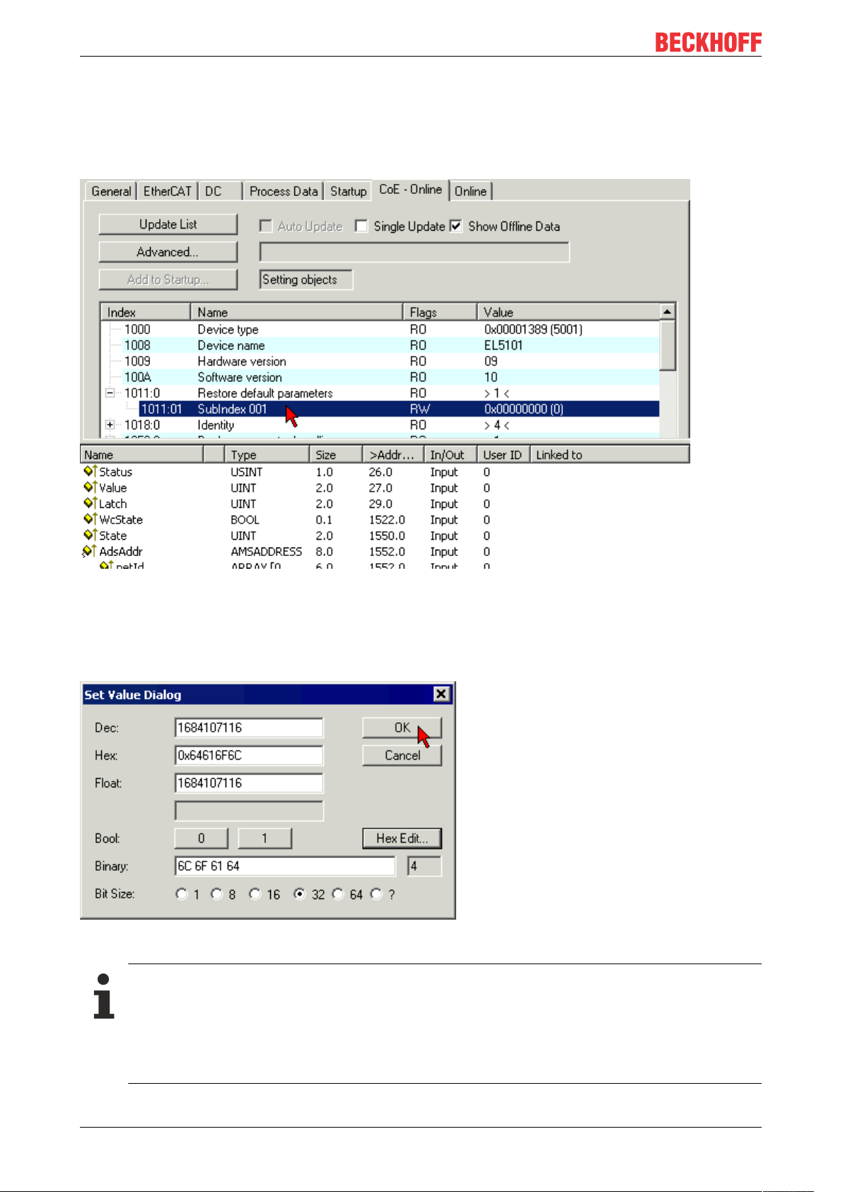
Commissioning and configuration
5.5 Restoring the delivery state
To restore the delivery state for backup objects in ELxxxx terminals / EPxxxx- and EPPxxxx boxes, the CoE
object Restore default parameters, SubIndex 001 can be selected in the TwinCAT System Manager (Config
mode).
Fig.16: Selecting the Restore default parameters PDO
Double-click on SubIndex 001 to enter the Set Value dialog. Enter the value 1684107116 in field Dec or the
value 0x64616F6C in field Hex and confirm with OK.
All backup objects are reset to the delivery state.
Fig.17: Entering a restore value in the Set Value dialog
Alternative restore value
In some older terminals / boxes the backup objects can be switched with an alternative restore
value:
Decimal value: 1819238756
Hexadecimal value: 0x6C6F6164
An incorrect entry for the restore value has no effect.
EPP4374-000246 Version: 1.1
Page 47

Appendix
6 Appendix
6.1 General operating conditions
Protection degrees (IP-Code)
The standard IEC 60529 (DIN EN 60529) defines the degrees of protection in different classes.
1. Number: dust protection and
touch guard
0 Non-protected
1 Protected against access to hazardous parts with the back of a hand. Protected against solid
2 Protected against access to hazardous parts with a finger. Protected against solid foreign ob-
3 Protected against access to hazardous parts with a tool. Protected against solid foreign objects
4 Protected against access to hazardous parts with a wire. Protected against solid foreign objects
5 Protected against access to hazardous parts with a wire. Dust-protected. Intrusion of dust is not
6 Protected against access to hazardous parts with a wire. Dust-tight. No intrusion of dust.
Definition
foreign objects of Ø50mm
jects of Ø12.5mm.
Ø2.5mm.
Ø1mm.
totally prevented, but dust shall not penetrate in a quantity to interfere with satisfactory operation
of the device or to impair safety.
2. Number: water* protection Definition
0 Non-protected
1 Protected against water drops
2 Protected against water drops when enclosure tilted up to 15°.
3 Protected against spraying water. Water sprayed at an angle up to 60° on either side of the ver-
4 Protected against splashing water. Water splashed against the disclosure from any direction
5 Protected against water jets
6 Protected against powerful water jets
7 Protected against the effects of temporary immersion in water. Intrusion of water in quantities
tical shall have no harmful effects.
shall have no harmful effects
causing harmful effects shall not be possible when the enclosure is temporarily immersed in water for 30min. in 1m depth.
*) These protection classes define only protection against water!
Chemical Resistance
The Resistance relates to the Housing of the IP 67 modules and the used metal parts. In the table below you
will find some typical resistance.
Character Resistance
Steam at temperatures >100°C: not resistant
Sodium base liquor
(ph-Value > 12)
Acetic acid not resistant
Argon (technical clean) resistant
at room temperature: resistant
> 40°C: not resistant
Key
• resistant: Lifetime several months
• non inherently resistant: Lifetime several weeks
• not resistant: Lifetime several hours resp. early decomposition
EPP4374-0002 47Version: 1.1
Page 48

Appendix
6.2 Accessories
Mounting
Ordering information Description
ZS5300-0001 Mounting rail (500mmx129mm)
Cables
A complete overview of pre-assembled cables for EtherCAT Box modules can be found here.
Ordering information Description
ZK2000-5xxx-xxxx
ZK2000-71xx-xxxx
ZK2000-6xxx-xxxx
ZK700x-xxxx-xxxx
Labeling material, protective caps
Ordering information Description
ZS5000-0010 Protective cap for M8 sockets, IP67 (50 pieces)
ZS5000-0020 Protective cap M12, IP67 (50 pieces)
ZS5100-0000 Inscription labels, unprinted, 4 strips of 10
ZS5000-xxxx Printed inscription labels on enquiry
Sensor cable M12 5-wire Link to website
Sensor cable M12 4-wire Link to website
EtherCAT P cable M8 Link to website
Tools
Ordering information Description
ZB8801-0000 Torque wrench for plugs, 0.4…1.0Nm
ZB8801-0001 Torque cable key for M8/ wrench size 9 for ZB8801-0000
ZB8801-0002 Torque cable key for M12/ wrench size 13 for ZB8801-0000
ZB8801-0003 Torque cable key for M12 field assembly/ wrench size 18 for ZB8801-0000
Further accessories
Further accessories can be found in the price list for fieldbus components from Beckhoff and online
at https://www.beckhoff.com.
EPP4374-000248 Version: 1.1
Page 49

Appendix
6.3 Version identification of EtherCAT devices
Designation
A Beckhoff EtherCAT device has a 14-digit designation, made up of
• family key
• type
• version
• revision
Example Family Type Version Revision
EL3314-0000-0016 EL terminal
(12 mm, nonpluggable connection
level)
ES3602-0010-0017 ES terminal
(12 mm, pluggable
connection level)
CU2008-0000-0000 CU device 2008 (8-port fast ethernet switch) 0000 (basic type) 0000
3314 (4-channel thermocouple
terminal)
3602 (2-channel voltage
measurement)
0000 (basic type) 0016
0010 (highprecision version)
0017
Notes
• The elements mentioned above result in the technical designation. EL3314-0000-0016 is used in the
example below.
• EL3314-0000 is the order identifier, in the case of “-0000” usually abbreviated to EL3314. “-0016” is the
EtherCAT revision.
• The order identifier is made up of
- family key (EL, EP, CU, ES, KL, CX, etc.)
- type (3314)
- version (-0000)
• The revision -0016 shows the technical progress, such as the extension of features with regard to the
EtherCAT communication, and is managed by Beckhoff.
In principle, a device with a higher revision can replace a device with a lower revision, unless specified
otherwise, e.g. in the documentation.
Associated and synonymous with each revision there is usually a description (ESI, EtherCAT Slave
Information) in the form of an XML file, which is available for download from the Beckhoff web site.
From 2014/01 the revision is shown on the outside of the IP20 terminals, see Fig. “EL5021 EL terminal,
standard IP20 IO device with batch number and revision ID (since 2014/01)”.
• The type, version and revision are read as decimal numbers, even if they are technically saved in
hexadecimal.
Identification number
Beckhoff EtherCAT devices from the different lines have different kinds of identification numbers:
Production lot/batch number/serial number/date code/D number
The serial number for Beckhoff IO devices is usually the 8-digit number printed on the device or on a sticker.
The serial number indicates the configuration in delivery state and therefore refers to a whole production
batch, without distinguishing the individual modules of a batch.
Structure of the serial number: KKYYFFHH
KK - week of production (CW, calendar week)
YY - year of production
FF - firmware version
HH - hardware version
EPP4374-0002 49Version: 1.1
Page 50

Appendix
Example with
Ser. no.: 12063A02: 12 - production week 12 06 - production year 2006 3A - firmware version 3A 02 hardware version 02
Exceptions can occur in the IP67 area, where the following syntax can be used (see respective device
documentation):
Syntax: D ww yy x y z u
D - prefix designation
ww - calendar week
yy - year
x - firmware version of the bus PCB
y - hardware version of the bus PCB
z - firmware version of the I/O PCB
u - hardware version of the I/O PCB
Example: D.22081501 calendar week 22 of the year 2008 firmware version of bus PCB: 1 hardware version
of bus PCB: 5 firmware version of I/O PCB: 0 (no firmware necessary for this PCB) hardware version of I/O
PCB: 1
Unique serial number/ID, ID number
In addition, in some series each individual module has its own unique serial number.
See also the further documentation in the area
• IP67: EtherCAT Box
• Safety: TwinSafe
• Terminals with factory calibration certificate and other measuring terminals
Examples of markings
Fig.18: EL5021 EL terminal, standard IP20 IO device with serial/ batch number and revision ID (since
2014/01)
EPP4374-000250 Version: 1.1
Page 51

Fig.19: EK1100 EtherCAT coupler, standard IP20 IO device with serial/ batch number
Appendix
Fig.20: CU2016 switch with serial/ batch number
Fig.21: EL3202-0020 with serial/ batch number 26131006 and unique ID-number 204418
EPP4374-0002 51Version: 1.1
Page 52

Appendix
Fig.22: EP1258-00001 IP67 EtherCAT Box with batch number/ date code 22090101 and unique serial
number 158102
Fig.23: EP1908-0002 IP67 EtherCAT Safety Box with batch number/ date code 071201FF and unique serial
number 00346070
Fig.24: EL2904 IP20 safety terminal with batch number/ date code 50110302 and unique serial number
00331701
Fig.25: ELM3604-0002 terminal with unique ID number (QR code) 100001051 and serial/ batch number
44160201
EPP4374-000252 Version: 1.1
Page 53

Appendix
6.3.1 Beckhoff Identification Code (BIC)
The Beckhoff Identification Code (BIC) is increasingly being applied to Beckhoff products to uniquely identify
the product. The BIC is represented as a Data Matrix Code (DMC, code scheme ECC200), the content is
based on the ANSI standard MH10.8.2-2016.
Fig.26: BIC as data matrix code (DMC, code scheme ECC200)
The BIC will be introduced step by step across all product groups.
Depending on the product, it can be found in the following places:
• on the packaging unit
• directly on the product (if space suffices)
• on the packaging unit and the product
The BIC is machine-readable and contains information that can also be used by the customer for handling
and product management.
Each piece of information can be uniquely identified using the so-called data identifier
(ANSIMH10.8.2-2016). The data identifier is followed by a character string. Both together have a maximum
length according to the table below. If the information is shorter, spaces are added to it. The data under
positions 1 to 4 are always available.
The following information is contained:
EPP4374-0002 53Version: 1.1
Page 54

Appendix
Item
Type of
no.
information
1 Beckhoff order
number
2 Beckhoff Traceability
Number (BTN)
3 Article description Beckhoff article
4 Quantity Quantity in packaging
5 Batch number Optional: Year and week
6 ID/serial number Optional: Present-day
7 Variant number Optional: Product variant
...
Explanation Data
Beckhoff order number 1P 8 1P072222
Unique serial number,
see note below
description, e.g.
EL1008
unit, e.g. 1, 10, etc.
of production
serial number system,
e.g. with safety products
number on the basis of
standard products
Number of digits
identifier
S 12 SBTNk4p562d7
1K 32 1KEL1809
Q 6 Q1
2P 14 2P401503180016
51S 12 51S678294104
30P 32 30PF971, 2*K183
incl. data identifier
Example
Further types of information and data identifiers are used by Beckhoff and serve internal processes.
Structure of the BIC
Example of composite information from item 1 to 4 and 6. The data identifiers are marked in red for better
display:
BTN
An important component of the BIC is the Beckhoff Traceability Number (BTN, item no.2). The BTN is a
unique serial number consisting of eight characters that will replace all other serial number systems at
Beckhoff in the long term (e.g. batch designations on IO components, previous serial number range for
safety products, etc.). The BTN will also be introduced step by step, so it may happen that the BTN is not yet
coded in the BIC.
NOTE
This information has been carefully prepared. However, the procedure described is constantly being further
developed. We reserve the right to revise and change procedures and documentation at any time and without prior notice. No claims for changes can be made from the information, illustrations and descriptions in
this information.
EPP4374-000254 Version: 1.1
Page 55

Appendix
6.4 Support and Service
Beckhoff and their partners around the world offer comprehensive support and service, making available fast
and competent assistance with all questions related to Beckhoff products and system solutions.
Beckhoff's branch offices and representatives
Please contact your Beckhoff branch office or representative for local support and service on Beckhoff
products!
The addresses of Beckhoff's branch offices and representatives round the world can be found on her internet
pages:
http://www.beckhoff.com
You will also find further documentation for Beckhoff components there.
Beckhoff Headquarters
Beckhoff Automation GmbH & Co. KG
Huelshorstweg 20
33415 Verl
Germany
Phone: +49 5246 963 0
Fax: +49 5246 963 198
e-mail: info@beckhoff.com
Beckhoff Support
Support offers you comprehensive technical assistance, helping you not only with the application of
individual Beckhoff products, but also with other, wide-ranging services:
• support
• design, programming and commissioning of complex automation systems
• and extensive training program for Beckhoff system components
Hotline: +49 5246 963 157
Fax: +49 5246 963 9157
e-mail: support@beckhoff.com
Beckhoff Service
The Beckhoff Service Center supports you in all matters of after-sales service:
• on-site service
• repair service
• spare parts service
• hotline service
Hotline: +49 5246 963 460
Fax: +49 5246 963 479
e-mail: service@beckhoff.com
EPP4374-0002 55Version: 1.1
Page 56

Page 57

More Information:
www.beckhoff.com/epp4374/
Beckhoff Automation GmbH & Co. KG
Hülshorstweg 20
33415 Verl
Germany
Phone: +49 5246 9630
info@beckhoff.com
www.beckhoff.com
 Loading...