

Page 1
Documentation
EP9214-0023 and EP9224-0023
Power Distribution for EtherCAT Box Modules
Version:
Date:
2.3.1
2018-04-10
Page 2

Page 3

Table of contents
Table of contents
1 Foreword ....................................................................................................................................................5
1.1 Notes on the documentation........................................................................................................... 5
1.2 Safety instructions .......................................................................................................................... 6
1.3 Documentation issue status............................................................................................................ 7
2 Product overview.......................................................................................................................................8
2.1 EtherCAT Box - Introduction........................................................................................................... 8
2.2 EP9214 - Introduction ................................................................................................................... 10
2.3 EP9224 - Introduction ................................................................................................................... 11
2.4 Technical data .............................................................................................................................. 12
3 Mounting and cabling .............................................................................................................................13
3.1 Mounting ....................................................................................................................................... 13
3.1.1 Dimensions ......................................................................................................................13
3.1.2 Mounting ..........................................................................................................................14
3.1.3 Nut torque for connectors ................................................................................................15
3.2 EtherCAT ...................................................................................................................................... 16
3.2.1 EtherCAT connection.......................................................................................................16
3.2.2 EtherCAT - Fieldbus LEDs...............................................................................................18
3.3 Power supply ................................................................................................................................ 20
3.3.1 Power Connection............................................................................................................20
3.3.2 Power LEDs .....................................................................................................................22
3.3.3 Power cable conductor losses M8 ...................................................................................23
3.3.4 Power cable 7/8" ..............................................................................................................24
3.3.5 Conductor losses 7/8" ......................................................................................................26
3.3.6 Power outputs ..................................................................................................................27
3.4 Cabling.......................................................................................................................................... 28
3.5 Status LEDs and status bits.......................................................................................................... 30
3.6 Monitoring and reset contacts....................................................................................................... 31
4 Comissioning and Configuration...........................................................................................................32
4.1 Inserting into the EtherCAT network............................................................................................. 32
4.2 Configuration via TwinCAT ........................................................................................................... 35
4.3 Operation with or without EtherCAT master ................................................................................. 43
4.4 Switch of behavior ........................................................................................................................ 44
4.4.1 Switch-off characteristics .................................................................................................44
4.4.2 Current limitation, switching the load circuits off ..............................................................46
4.4.3 Setting the current limitation ............................................................................................47
4.4.4 Status LEDs and status bits.............................................................................................48
4.5 EP9214-0023................................................................................................................................ 50
4.5.1 EP9214-0023 - Object description ...................................................................................50
4.5.2 EP9214-0023 - Process image ........................................................................................65
4.6 EP9224-0023................................................................................................................................ 66
4.6.1 EP9224-0023 - Diagnostic functions................................................................................66
4.6.2 EP9224-0023 - Object description ...................................................................................79
4.6.3 EP9224-0023 - Process image ......................................................................................106
4.7 Restoring the delivery state ........................................................................................................ 107
5 Appendix ................................................................................................................................................109
5.1 General operating conditions...................................................................................................... 109
5.2 EtherCAT Box- / EtherCATPBox - Accessories........................................................................ 110
EP9214-0023 and EP9224-0023 3Version: 2.3.1
Page 4

Table of contents
5.3 Support and Service ................................................................................................................... 111
EP9214-0023 and EP9224-00234 Version: 2.3.1
Page 5

Foreword
1 Foreword
1.1 Notes on the documentation
Intended audience
This description is only intended for the use of trained specialists in control and automation engineering who
are familiar with the applicable national standards.
It is essential that the documentation and the following notes and explanations are followed when installing
and commissioning these components.
It is the duty of the technical personnel to use the documentation published at the respective time of each
installation and commissioning.
The responsible staff must ensure that the application or use of the products described satisfy all the
requirements for safety, including all the relevant laws, regulations, guidelines and standards.
Disclaimer
The documentation has been prepared with care. The products described are, however, constantly under
development.
We reserve the right to revise and change the documentation at any time and without prior announcement.
No claims for the modification of products that have already been supplied may be made on the basis of the
data, diagrams and descriptions in this documentation.
Trademarks
Beckhoff®, TwinCAT®, EtherCAT®, Safety over EtherCAT®, TwinSAFE®, XFC® and XTS® are registered
trademarks of and licensed by Beckhoff Automation GmbH.
Other designations used in this publication may be trademarks whose use by third parties for their own
purposes could violate the rights of the owners.
Patent Pending
The EtherCAT Technology is covered, including but not limited to the following patent applications and
patents: EP1590927, EP1789857, DE102004044764, DE102007017835 with corresponding applications or
registrations in various other countries.
The TwinCAT Technology is covered, including but not limited to the following patent applications and
patents: EP0851348, US6167425 with corresponding applications or registrations in various other countries.
EtherCAT® is registered trademark and patented technology, licensed by Beckhoff Automation GmbH,
Germany
Copyright
© Beckhoff Automation GmbH & Co. KG, Germany.
The reproduction, distribution and utilization of this document as well as the communication of its contents to
others without express authorization are prohibited.
Offenders will be held liable for the payment of damages. All rights reserved in the event of the grant of a
patent, utility model or design.
EP9214-0023 and EP9224-0023 5Version: 2.3.1
Page 6
Foreword
1.2 Safety instructions
Safety regulations
Please note the following safety instructions and explanations!
Product-specific safety instructions can be found on following pages or in the areas mounting, wiring,
commissioning etc.
Exclusion of liability
All the components are supplied in particular hardware and software configurations appropriate for the
application. Modifications to hardware or software configurations other than those described in the
documentation are not permitted, and nullify the liability of Beckhoff Automation GmbH & Co. KG.
Personnel qualification
This description is only intended for trained specialists in control, automation and drive engineering who are
familiar with the applicable national standards.
Description of symbols
In this documentation the following symbols are used with an accompanying safety instruction or note. The
safety instructions must be read carefully and followed without fail!
DANGER
WARNING
CAUTION
Attention
Note
Serious risk of injury!
Failure to follow the safety instructions associated with this symbol directly endangers the
life and health of persons.
Risk of injury!
Failure to follow the safety instructions associated with this symbol endangers the life and
health of persons.
Personal injuries!
Failure to follow the safety instructions associated with this symbol can lead to injuries to
persons.
Damage to the environment or devices
Failure to follow the instructions associated with this symbol can lead to damage to the environment or equipment.
Tip or pointer
This symbol indicates information that contributes to better understanding.
EP9214-0023 and EP9224-00236 Version: 2.3.1
Page 7
1.3 Documentation issue status
Version Comment
2.3.1 • chapter Switch of behavior updated
• Nut torque for connectors updated
2.3.0 • Cabling added
2.2.0 • Operation with or without EtherCAT master updated
2.1.0 • Power Connection updated
2.0.0 • migration
• chapter mounting and cabling updated
• chapter nut torque for connectors extended
• chapter switch off behavior updated
• object descriptions updated
1.1.0 • EP9224-0023 added
1.0.0 • first release
0.1 • preliminary version (only German available)
Firm and hardware version
Foreword
The documentation refers to the firm and hardware status that was valid at the time it was prepared.
The properties of the modules are subject to continuous development and improvement. Modules having
earlier production statuses cannot have the same properties as modules with the latest status. Existing
properties, however, are always retained and are not changed, so that these modules can always be
replaced by new ones.
Documentation
version
2.1.0 09 11 04 10
2.0.0 09 10 04 10
1.1.0 09 06 04 06
1.0.0 07 03 - -
0.1 07 03 - -
The firmware and hardware version (delivery state) can be found in the batch number (D number) printed at
the side of the EtherCAT Box.
Syntax of the batch number (D number)
WWYYFFHH
WW - week of production (calendar week)
YY - year of production
FF - firmware version
HH - hardware version
EP9214-0023 EP9224-0023
firmware hardware firmware hardware
Example with ser. no.: 55 09 01 00:
55 - week of production 55
09 - year of production 2009
01 - firmware version 01
00 - hardware version 00
EP9214-0023 and EP9224-0023 7Version: 2.3.1
Page 8

Product overview
2 Product overview
2.1 EtherCAT Box - Introduction
The EtherCAT system has been extended with EtherCAT Box modules with protection class IP67. Through
the integrated EtherCAT interface the modules can be connected directly to an EtherCAT network without an
additional Coupler Box. The high-performance of EtherCAT is thus maintained into each module.
The extremely low dimensions of only 126x30x26.5 mm (hxw xd) are identical to those of the Fieldbus
Box extension modules. They are thus particularly suitable for use where space is at a premium. The small
mass of the EtherCAT modules facilitates applications with mobile I/O interface (e.g. on a robot arm). The
EtherCAT connection is established via screened M8connectors.
Fig.1: EtherCAT Box Modules within an EtherCAT network
The robust design of the EtherCAT Box modules enables them to be used directly at the machine. Control
cabinets and terminal boxes are now no longer required. The modules are fully sealed and therefore ideally
prepared for wet, dirty or dusty conditions.
Pre-assembled cables significantly simplify EtherCAT and signal wiring. Very few wiring errors are made, so
that commissioning is optimized. In addition to pre-assembled EtherCAT, power and sensor cables, fieldconfigurable connectors and cables are available for maximum flexibility. Depending on the application, the
sensors and actuators are connected through M8 or M12connectors.
The EtherCAT modules cover the typical range of requirements for I/O signals with protection class IP67:
• digital inputs with different filters (3.0ms or 10μs)
• digital outputs with 0.5 or 2A output current
• analog inputs and outputs with 16bit resolution
• Thermocouple and RTD inputs
• Stepper motor modules
XFC (eXtreme Fast Control Technology) modules, including inputs with time stamp, are also available.
EP9214-0023 and EP9224-00238 Version: 2.3.1
Page 9
Fig.2: EtherCAT Box with M8 connections for sensors/actuators
Product overview
Fig.3: EtherCAT Box with M12 connections for sensors/actuators
Basic EtherCAT documentation
You will find a detailed description of the EtherCAT system in the Basic System Documen-
Note
tation for EtherCAT, which is available for download from our website (www.beckhoff.com)
under Downloads.
XML files
You will find XML files (XML Device Description Files) for Beckhoff EtherCAT modules on
Note
our website (www.beckhoff.com) under Downloads, in the Configuration Files area.
EP9214-0023 and EP9224-0023 9Version: 2.3.1
Page 10
Product overview
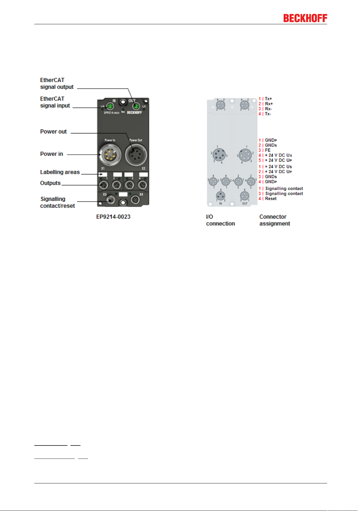
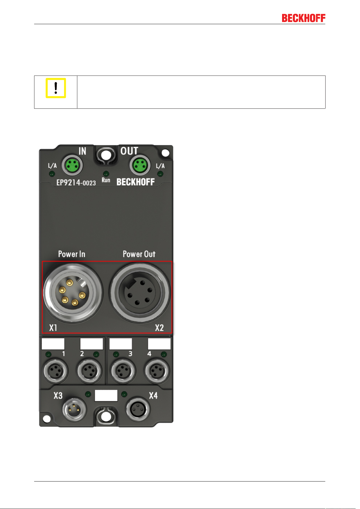
2.2 EP9214 - Introduction
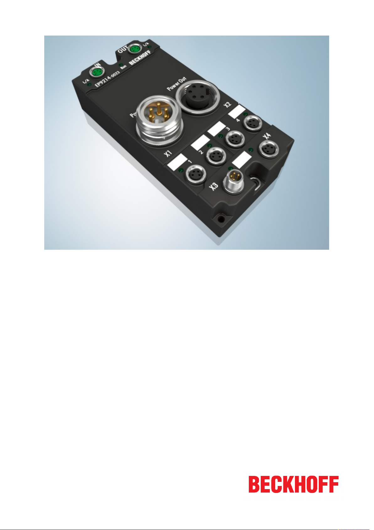
Fig.4: EP9214
Power distribution for EtherCAT Box (24VDC)
The EP9214-0023 enables connection of four power supply branches. In each branch the current
consumption for the control voltage US and the peripheral voltage UP is monitored, limited, and, if necessary,
switched off.
The power distribution is supplied via a 7/8" connector with up to 16A (per voltage supply US/UP). Several
modules can be configured in a cascade arrangement. In the event of a short-circuit in one of the four
outputs, the affected output is switched off. The supply for the other branches remains active. The switch-off
and control is done in such a way that the input voltage does not fall below 21V or other modules are going
down, caused by undervoltage.
During startup consumers with large capacities can be added without problem.
The master can read diagnostic messages from the individual channels via the EtherCAT interface.
Independent switching of individual consumer branches is also possible via the EtherCAT master.
In delivery state the eight outputs of the box (4 times Us, 4 times Up) are activated to enable operation
without EtherCAT.
After an error caused the switch off of a channel, this channel remains switched of when you try to switch it
on again and has to be set back actively by the EtherCAT master or a hardware reset at the box (lower M8
socket).
Quick links
Installation [}13]
Configuration [}32]
EP9214-0023 and EP9224-002310 Version: 2.3.1
Page 11
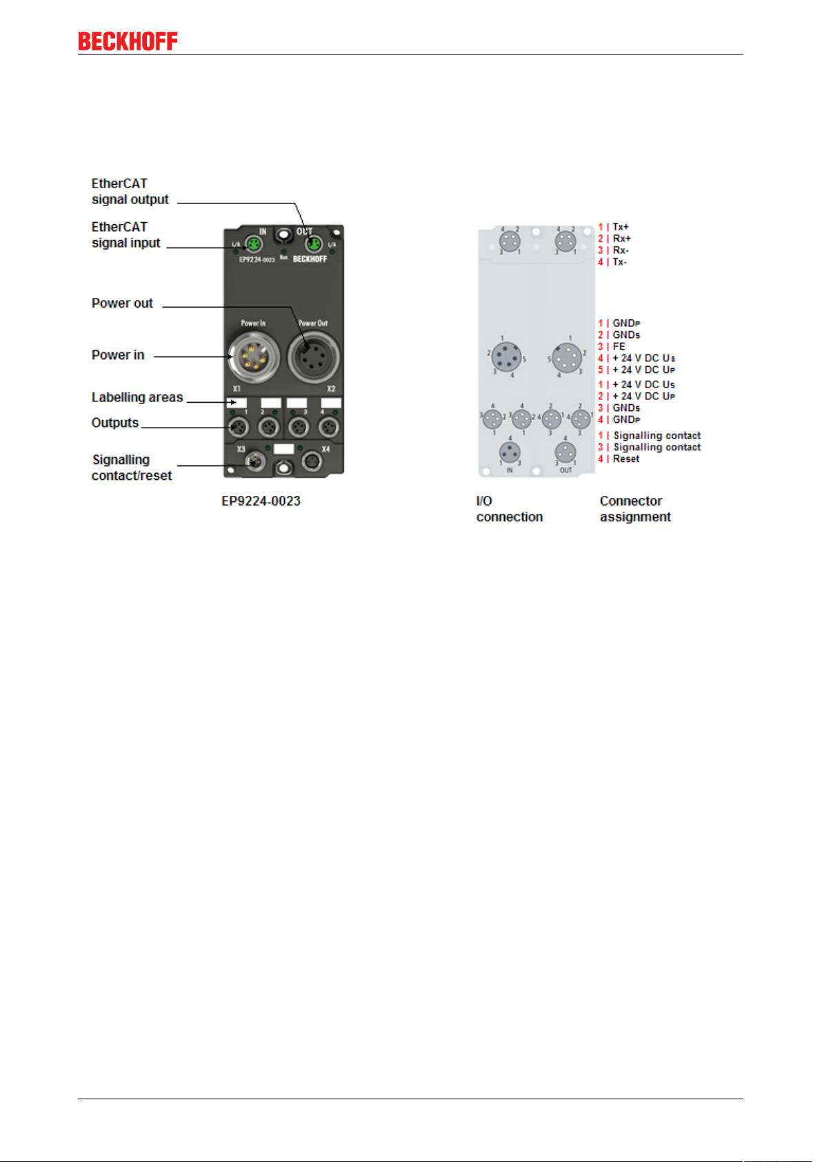
2.3 EP9224 - Introduction
Product overview
Fig.5: EP9224
Power distribution for EtherCAT Box (24VDC) with data logging
The EP9224-0023 enables connection of four power supply branches. In each branch the current
consumption for the control voltage US and the peripheral voltage UP is monitored, limited, and, if necessary,
switched off.
The power distribution is supplied via a 7/8" connector with up to 16 A (per voltage supply US/UP). Several
modules can be configured in a cascade arrangement. In the event of a short-circuit in one of the four
outputs, the affected output is switched off. The supply for the other branches remains active. The switch-off
and control is done in such a way that the input voltage does not fall below 21 V or other modules are going
down, caused by undervoltage.
During startup consumers with large capacities can be added without problem.
The master can read diagnostic messages from the individual channels via the EtherCAT interface.
Independent switching of individual consumer branches is also possible via the EtherCAT master.
In delivery state the eight outputs of the box (4 times Us, 4 times Up) are activated to enable operation
without EtherCAT.
After an error caused the switch off of a channel, this channel remains switched of when you try to switch it
on again and has to be set back actively by the EtherCAT master or a hardware reset at the box (lower M8
socket).
Additional to this basic functionality that is also provided by EP9214, the EP9224 displays the voltage values
of PowerIn supply and all current values of inputs and outputs within the process data.
The box has got an internal log file, that is writing the system values continuously into a ring buffer. This data
logging has to be activated at the startup.
In error case it is stopped, so a history of the system parameters from before the error case can be read out.
This enables a much quicker error localization.
EP9214-0023 and EP9224-0023 11Version: 2.3.1
Page 12

Product overview
Quick links
Installation [}13]
Configuration [}35]
2.4 Technical data
Technical data EP9214-0023 EP9224-0023
Rated voltage 24VDC (-15%/ +20%)
Power supply Feed: Plug 7/8", max. 16A for each Us/Up
Onward connection: Socket 7/8", max. 16A for each Us/Up
Number of load outputs 4 x M8, for each Us and Up
Voltage drop VON in the load
circuits
Parallel connection of several load
outputs
Overload switch-off dependent on selected load curve (20ms at 3xIN, see time/current
Temperature switch-off Internal temperature switch-off
Switch-on delay 10, 100 or 200ms (adjustable via CoE)
Selectivity in case of an error, the channel concerned is switched off
Signalling contact 1
Reset contact 1
Connections for signal and reset
contacts
Fieldbus EtherCAT
Fieldbus connection 2 x M8 sockets, screened, marked green
Electrical isolation Control voltage/fieldbus: 500V
Supply of the module circuitry from the control voltage Us
Current consumption of the module
circuitry
Process image Inputs: 5 x 16bit
Data logging - 40 samples ( 1ms - 1000ms
Permissible ambient temperature
during operation
Permissible ambient temperature
during storage
Vibration / shock resistance conforms to EN60068-2-6 / EN60068-2-27
EMC immunity/emission conforms to EN61000-6-2 / EN61000-6-4
Dimensions 126mm x 60mm x 40 mm
Weight approx. 450g
Installation position variable
Protection class IP65, IP66, IP67 (according to EN 60529)
Approvals CE, UL in preparation
90mV / Ampere
not permissible
characteristics)
in : 1 x M8 plug
out : 1 x M8 socket
typically 110mA from Us,
typically 40mA from Up
Outputs: 5 x 16bit
-25°C ... +60°C
-25 °C... +85°C
Inputs: 16x16Bit
Outputs: 5x16Bit
sample time)
EP9214-0023 and EP9224-002312 Version: 2.3.1
Page 13

3 Mounting and cabling
3.1 Mounting
3.1.1 Dimensions
Mounting and cabling
Fig.6: Dimensions of the EtherCAT Box Modules
All dimensions are given in millimeters.
EP9214-0023 and EP9224-0023 13Version: 2.3.1
Page 14
Mounting and cabling
Housing properties
EtherCAT Box lean body wide body
Housing material PA6 (polyamide)
Casting compound Polyurethane
Mounting two fastening holes Ø3mm for M3 two fastening holes Ø3mm for M3
two fastening holes Ø4,5mm for M4
Metal parts Brass, nickel-plated
Contacts CuZn, gold-plated
Power feed through max. 4A
Installation position variable
Protection class IP65, IP66, IP67 (conforms to EN 60529) when screwed together
Dimensions
(HxWxD)
Weight approx. 125g, depending on module
ca. 126 x 30 x 26,5mm ca. 126 x 60 x 26,5mm
approx. 250g, depending on module type
type
3.1.2 Mounting
EP9214 modules are mounted using two M3 bolts in the mounting holes located in the corners or using two
M4 bolts in the centrally located mounting holes.
The bolts must be longer than 15 mm. The mounting holes in the modules have no thread.
Protect connectors against soiling
Protect all module connections from soiling during installation!The protection classes IP65,
Note
IP66, IP67 (in accordance with EN 60529) are ensured only if all connectors are wired or
sealed! Unused connectors must be sealed with suitable protective caps (see Beckhoff catalogue for connector sets and protective caps)!
Cooling plate
The EP9214 module has a cooling plate on the underside. For the effective dissipation of
Note
Note when mounting that the overall height is increased further by the fieldbus connections. See the
Accessories section
the resultant power loss, the box must be bolted to a metal base, e.g. the machine bed, if
possible making contact over the entire surface.A temperature-related automatic switch-off
of the box can occur if care is not taken to ensure that the power loss from the module is
dissipated via the cooling plate. A corresponding temperature error bit is then set!
EP9214-0023 and EP9224-002314 Version: 2.3.1
Page 15
Mounting and cabling
3.1.3 Nut torque for connectors
M8 connectors
It is recommended to pull the M8 connectors tight with a nut torque of 0.4 Nm. When using the torque control
screwdriver ZB8800 is also a max. torque of 0.5Nm permissible.
Fig.7: EtherCAT Box with M8 connectors
M12 connectors
It is recommended to pull the M12 connectors tight with a nut torque of 0.6 Nm.
Fig.8: EtherCAT Box with M8 and M12 connectors
EP9214-0023 and EP9224-0023 15Version: 2.3.1
Page 16
Mounting and cabling
7/8" plug connectors
We recommend fastening the 7/8" plug connectors with a torque of 1.5Nm.
Fig.9: 7/8" plug connectors
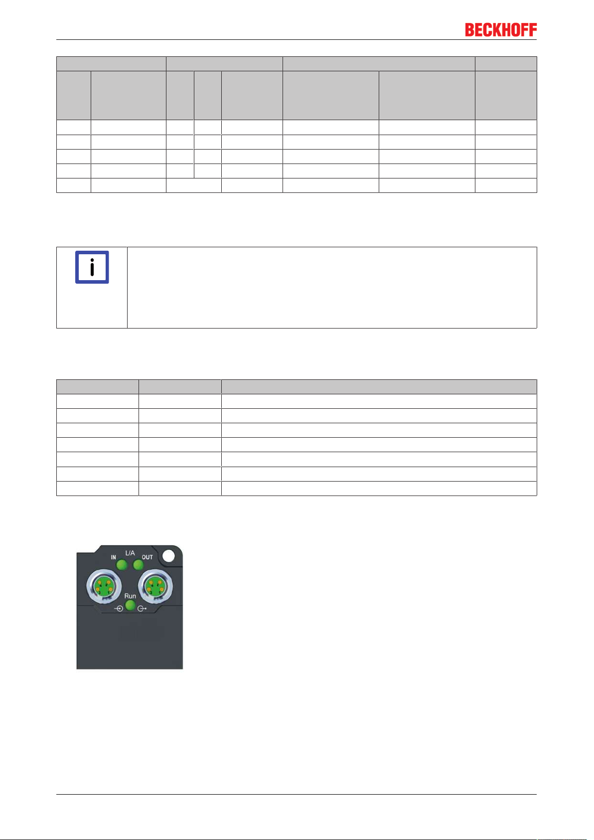
Torque socket wrenches
Fig.10: ZB8801 torque socket wrench
Ensure the right torque
Use the torque socket wrenches available by Beckhoff to pull the connectors tight (ZB8800,
Note
ZB8801-0000)!
3.2 EtherCAT
3.2.1 EtherCAT connection
For the incoming and ongoing EtherCAT connection,
• the EtherCAT Box (EPxxxx) has two M8 sockets, marked in green
• the Coupler Box (FBB-x110) has two M12 sockets
EP9214-0023 and EP9224-002316 Version: 2.3.1
Page 17

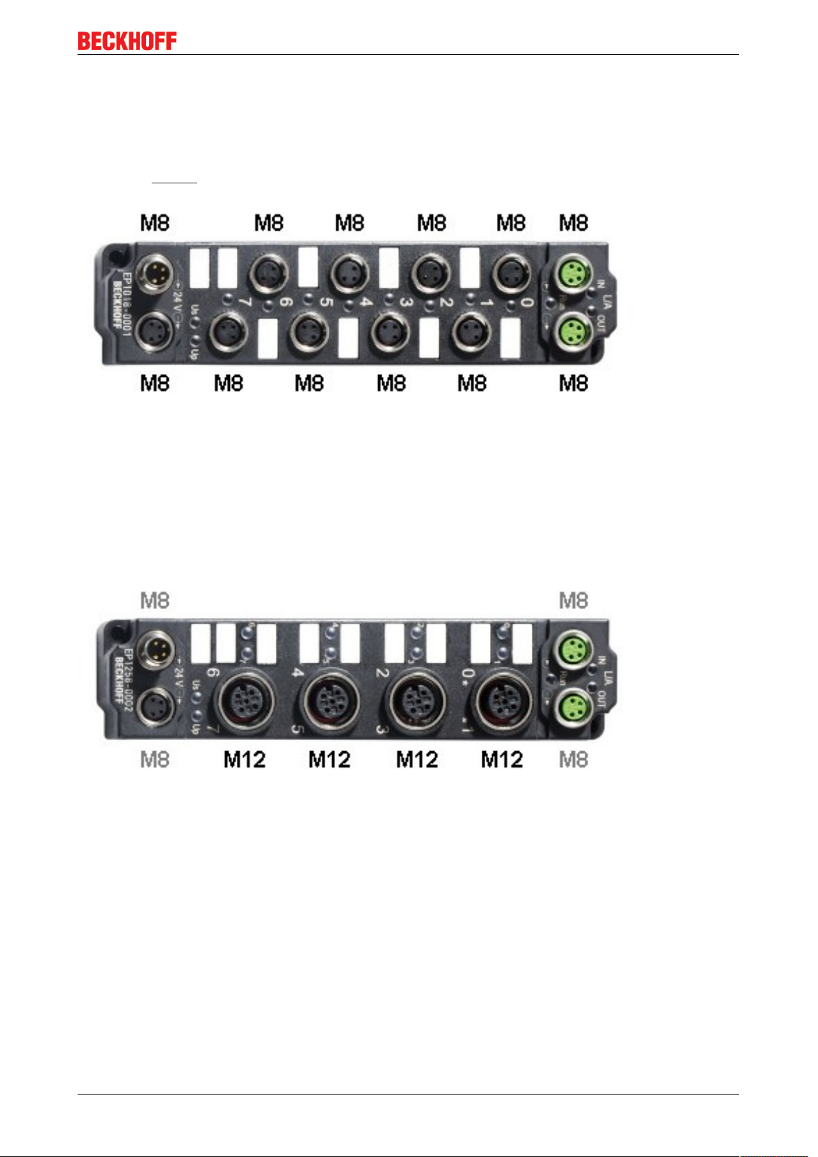
Fig.11: EtherCAT Box: M8 (30mm housing)
Mounting and cabling
Fig.12: EtherCAT Box: M8 60mm housing (EP9214 for example )
Fig.13: Coupler Box: M12
Assignment
There are various different standards for the assignment and colors of connectors and cables for Ethernet/
EtherCAT.
EP9214-0023 and EP9224-0023 17Version: 2.3.1
Page 18
Mounting and cabling
Ethernet/EtherCAT Plug connector Cable Standard
Signal Description M8 M12 RJ45
Tx + Transmit Data+ Pin 1 Pin 1 Pin 1 yellow
Tx - Transmit Data- Pin 4 Pin 3 Pin 2 orange
Rx + Receive Data+ Pin 2 Pin 2 Pin 3 white
Rx - Receive Data- Pin 3 Pin 4 Pin 6 blue
1
ZB9010, ZB9020,
ZB9030, ZB9032,
ZK1090-6292,
ZK1090-3xxx-xxxx
2
2
2
2
ZB9031 and old
versions
of ZB9030, ZB9032,
ZK1090-3xxx-xxxx
orange/white
orange
blue/white
3
blue
3
3
3
TIA-568B
white/orange
orange
white/green
green
Shield Shield Housing Shroud Screen Screen Screen
1
) colored markings according to EN 61918 in the four-pin RJ45 connector ZS1090-0003
2
) wire colors according to EN 61918
3
) wire colors
Assimilation of color coding for cable ZB9030, ZB9032 and ZK1090-3xxxxxxxx (with M8 connectors)
Note
For unification the prevalent cables ZB9030, ZB9032 and ZK1090-3xxx-xxxx this means
the pre assembled cables with M8 connectors were changed to the colors of EN61918 (yellow, orange, white, blue).So different color coding exists. But the electrical properties are
absolutely identical.
EtherCAT connectors
The following connectors can be supplied for use in Beckhoff EtherCAT systems.
Designation Plug connector Comment
ZS1090-0003 RJ45 four-pin, IP20, for field assembly
ZS1090-0004 M12 four-pin, IP67, for field assembly
ZS1090-0005 RJ45 eight-pin, IP20, for field assembly, suitable for GigaBit Ethernet
ZS1090-0006 M8 male four-pin, IP67, for field assembly, for ZB903x cable
ZS1090-0007 M8 female four-pin, IP67, for field assembly, for ZB903x cable
ZS1090-1006 M8 male four-pin, IP67, for field assembly up to OD = 6.5mm
ZS1090-1007 M8 female four-pin, IP67, for field assembly up to OD = 6.5mm
3.2.2 EtherCAT - Fieldbus LEDs
Fig.14: EtherCAT-LEDs
EP9214-0023 and EP9224-002318 Version: 2.3.1
Page 19

LED display
LED Display Meaning
IN L/A off no connection to the preceding EtherCAT module
Lit LINK: connection to the preceding EtherCAT module
flashing ACT: Communication with the preceding EtherCAT module
OUT L/A off no connection to the following EtherCAT module
Lit LINK: connection to the following EtherCAT module
flashing ACT: Communication with the following EtherCAT module
Run off Status of the EtherCAT module is Init
flashes quickly Status of the EtherCAT module is pre-operational
flashes slowly Status of the EtherCAT module is safe-operational
Lit Status of the EtherCAT module is operational
EtherCAT statuses
The various statuses in which an EtherCAT module may be found are described in the Ba-
Note
sic System Documentation for EtherCAT, which is available for download from our website
(www.beckhoff.com) under Downloads.
Mounting and cabling
EP9214-0023 and EP9224-0023 19Version: 2.3.1
Page 20
Mounting and cabling
3.3 Power supply
3.3.1 Power Connection
Use cables with suitable cross-sections!
Ensure that the cross-sections of the cables employed are suitable for the load circuit in-
Attention
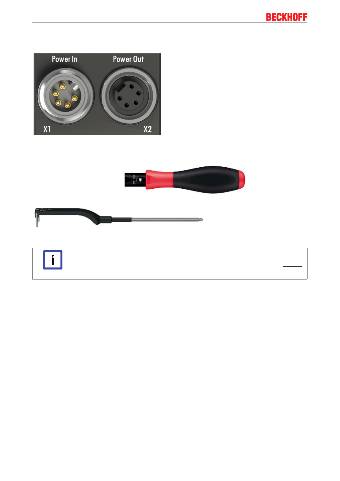
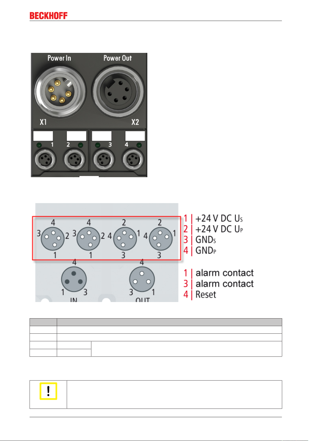
The supply voltages are fed and relayed onward via two 7/8" connectors in the center of the modules:
• Power In: left-hand 7/8" plug for the feed-in of supply voltages
• Power Out: right-hand 7/8" socket for the onward feeding of supply voltages
puts and outputs and the respective rated current being used!
Fig.15: EP9214-0023 - 7/8" connectors
The contacts of the 7/8" plug connectors can conduct a maximum current of 16A (40°C).
Two LEDs next to the device identifier label indicate the status of the supply voltages.
EP9214-0023 and EP9224-002320 Version: 2.3.1
Page 21
Pin assignment
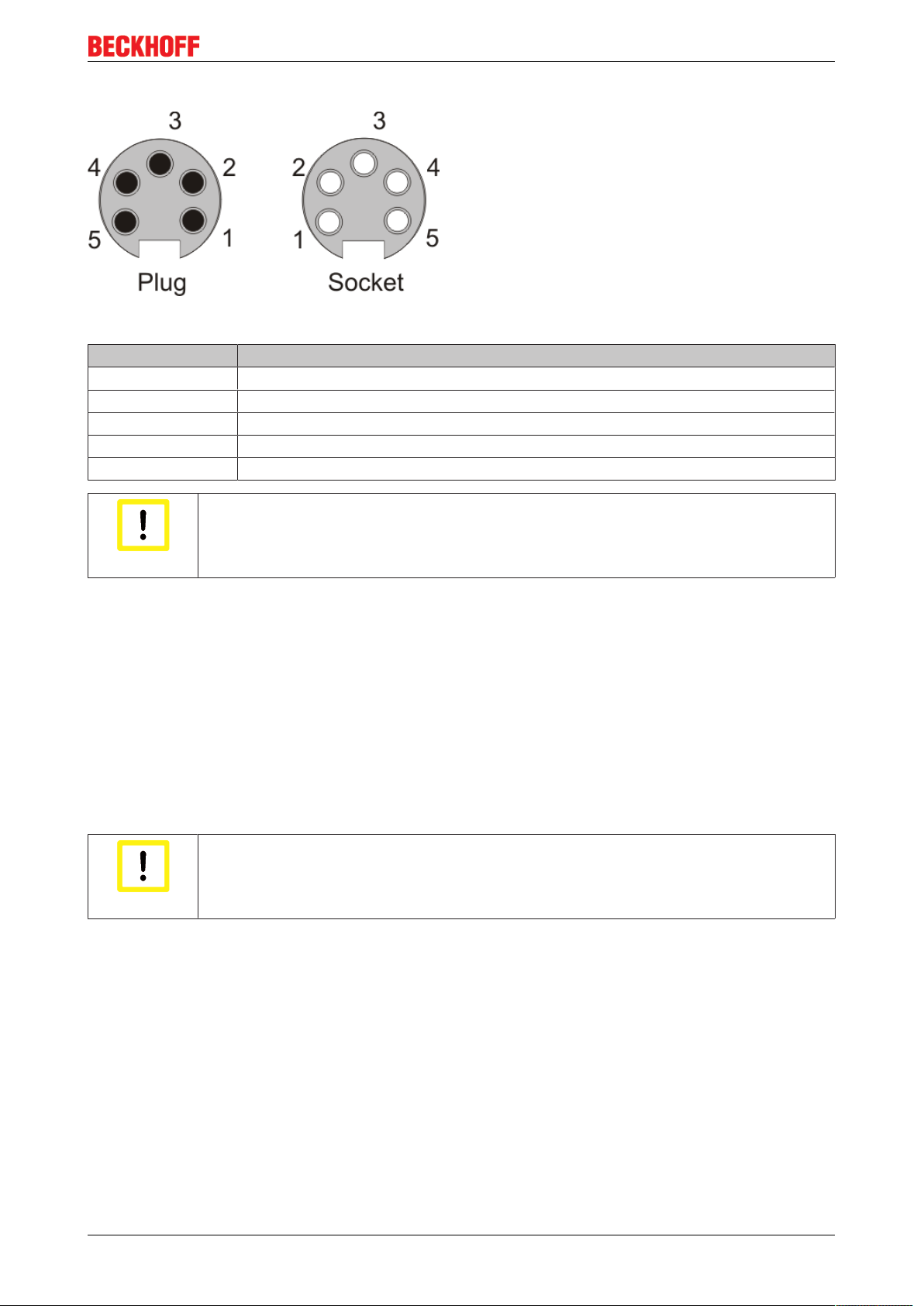
Fig.16: Pin assignment of 7/8" plug connectors
Contact Voltage
1 GND Up
2 GND Us
3 FE (Functional earth), (as well as contact at central mounting holes)
4 Control voltage Us, +24V
5 Peripheral voltage Up, +24V
DC
DC
Mounting and cabling
Do not confuse the power output with the EtherCAT connection!
Never connect the power cables (M8, 24 VDC) to the green-marked EtherCAT sockets of
the EtherCAT Box Modules. This can cause the destruction of the modules!
Attention
Control voltage Us: 24V
DC
The fieldbus and the processor logic are supplied from the 24 VDC control voltage Us. The control voltage is
electrically isolated from the fieldbus circuitry.
Peripheral voltage Up: 24V
DC
The peripheral voltage Up is monitored and fed to the power outputs, but is not used in the EP9214.
Redirection of the supply voltages
The power connections Power In and Power Out are bridged in the module. Hence, the supply voltages Us
and Up can be passed from EtherCAT Box to EtherCAT Box in a simple manner.
Observe the maximum current of the 7/8" plug connectors!
Also ensure when relaying the supply voltages Us and Up onward that the maximum per-
Attention
missible current of 16 A / 40 °C for each 7/8" plug connector is not exceeded!
EP9214-0023 and EP9224-0023 21Version: 2.3.1
Page 22
Mounting and cabling
3.3.2 Power LEDs
Status-LEDs for the power supply
LED Display Meaning
Us (control voltage) off The power supply voltage, Us, is
not present
Green illuminated The power supply voltage, Us, is
present
Up (peripheral voltage) off The power supply voltage, Up, is
not present
Green illuminated The power supply voltage, Up, is
present
EP9214-0023 and EP9224-002322 Version: 2.3.1
Page 23

Mounting and cabling
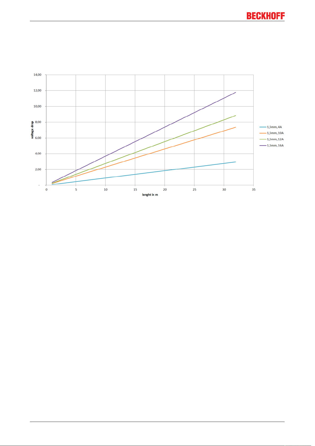
3.3.3 Power cable conductor losses M8
The ZK2020-xxxx-yyyy power cables should not exceed the total length of 15m at 4A (with continuation).
When planning the cabling, note that at 24V nominal voltage, the functionality of the module can no longer
be assured if the voltage drop reaches 6V. Variations in the output voltage from the power supply unit must
also be taken into account.
Fig.17: Power cable conductor losses
Example
8m power cable with 0.34mm² cross-section has a voltage drop of 3.2V at 4A.
EP92x4 Power Distribution Modules
With EP9214 and EP9224 Power Distribution Modules intelligent concepts for voltage sup-
Note
ply are available. Further information may be found under www.beckhoff.com/EP9224.
EP9214-0023 and EP9224-0023 23Version: 2.3.1
Page 24

Mounting and cabling
3.3.4 Power cable 7/8"
Fig.18: Power cable 7/8"
Technical data
Technical data
Rated voltage according to IEC61076-2-101 300V (according to IEC61076-2-101)
Contamination level according to IEC60664-1 3/2 (according to IEC60664-1)
Insulation resistance IEC60512-2 >109W
Current carrying capacity according to
IEC60512-3
Volume resistance according to IEC60512-2 < 5mW
Protection class conforms to IEC60529 IP65/66/67, when screwed together
Permissible ambient temperature -30°C to +80°C
Material properties TPE-U (PUR) halogen-free according to DINVDE0472
Approbations UL
Cable outside diameter 7.80 ± 0.20mm
Bending radius min. 6xD (external diameter)
Parameter Max. speed 5m/s, max. acceleration 10m/s²
Number of cycles At least 10million cycles with a max. travel path of 20
16A at 40°C (according to IEC60512-3)
Part815,
flame-retardant according to cULus 20549
meters
EP9214-0023 and EP9224-002324 Version: 2.3.1
Page 25

Ordering data
Mounting and cabling
Order identifier Power cable Screw type
connector
ZK2030-1200-0010 Straight socket, open end 7/8" 5-pin 1,50mm
Contacts Cross-sec-
tion
2
Length
1.00m
ZK2030-1200-0030 3.00m
ZK2030-1200-0050 5.00m
ZK2030-1200-0100 10.00m
ZK2030-1400-0010 Angled socket, open end 1.00m
ZK2030-1400-0030 3.00m
ZK2030-1400-0050 5.00m
ZK2030-1400-0100 10.00m
ZK2030-1112-0010 Straight socket, straight
ZK2030-1112-0030 3.00m
plug
1.00m
ZK2030-1112-0050 5.00m
ZK2030-1112-0100 10.00m
ZK2030-1314-0010 Angled socket, angled
ZK2030-1314-0030 3.00 m
plug
1.00m
ZK2030-1314-0050 5.00m
ZK2030-1314-0100 10.00m
Further available power cables and the associated data sheets can be found in the Beckhoff catalogue or on
our website (http://www.beckhoff.com).
EP9214-0023 and EP9224-0023 25Version: 2.3.1
Page 26
Mounting and cabling
3.3.5 Conductor losses 7/8"
In the case of the power cables ZK2030-xxxx-yyy, a total length of 15m should not be exceeded at 16A.
When wiring, note that with a rated voltage of 24V the function of the modules can no longer be guaranteed
from a voltage drop of 6V. Variations in the output voltage from the power supply unit must also be taken
into account.
Fig.19: ZK2030-xxxx-yyy - Conductor losses
Alternatively, larger cable cross-section can be used, e.g. 2.5mm2.
EP9214-0023 and EP9224-002326 Version: 2.3.1
Page 27
Mounting and cabling
3.3.6 Power outputs
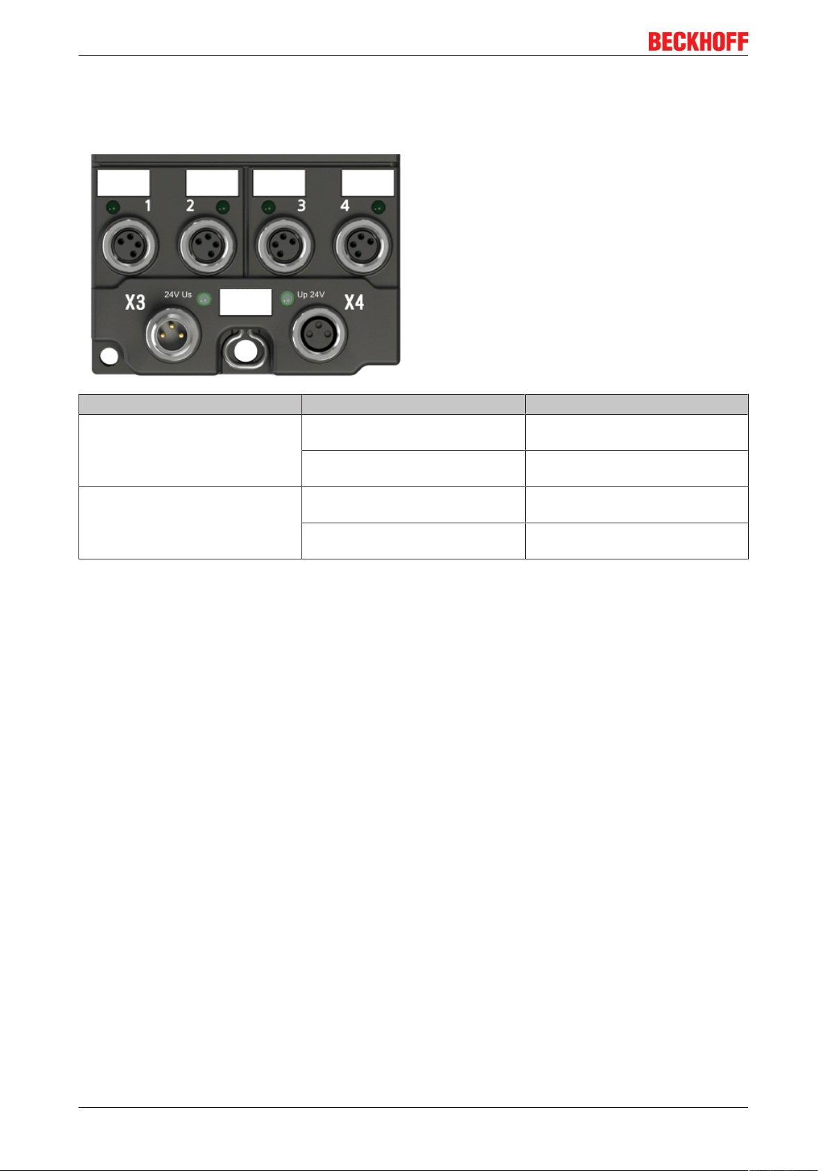
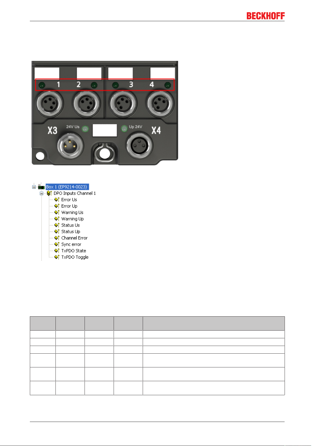
The supply voltages are output via four 4-pole M8 sockets in the lower third of the modules (1, 2, 3 and 4).
Fig.20: M8 sockets
Pin assignment
Fig.21: Pin assignment of the M8 sockets
Contact Voltage
1 Control voltage Us, +24V
2 Peripheral voltage Up, +24V
DC
DC
3 GNDs* *) can be internally connected to one another depending on the connected
4 GNDp*
module: see individual module descriptions
The contacts of the M8 plug connectors can conduct a maximum current of 4A.
A LED indicates the status of the power outputs.
Do not confuse the power outputs with the EtherCAT connection
Never connect the power cables (M8, 24VDC) to the green-marked EtherCAT sockets of the
Attention
EP9214-0023 and EP9224-0023 27Version: 2.3.1
EtherCAT Box Modules. This can cause the destruction of the modules!
Page 28

Mounting and cabling
Control voltage Us: 24V
DC
Power is supplied to the fieldbus, the processor logic, the inputs and the sensors from the control voltage Us
(24VDC). The control voltage is electrically isolated from the fieldbus circuitry.
Peripheral voltage Up: 24V
DC
The peripheral voltage Up (24VDC) supplies the digital outputs; it can be brought in separately. Hence, if the
load voltage is switched off, the fieldbus function as well as the supply and function of the inputs are
retained.
Electrical isolation
The grounds of the control voltage (GNDs) and peripheral voltage (GNDp) are electrically isolated from each
other in order to ensure the electrical isolation of the peripheral devices on Up from the control voltage.
The electrical isolation can be nullified
If you connect digital and analog EtherCAT Box Modules directly to one another via fourpole power lines, then there may no longer be any electrical isolation due to the connected
Attention
boxes!
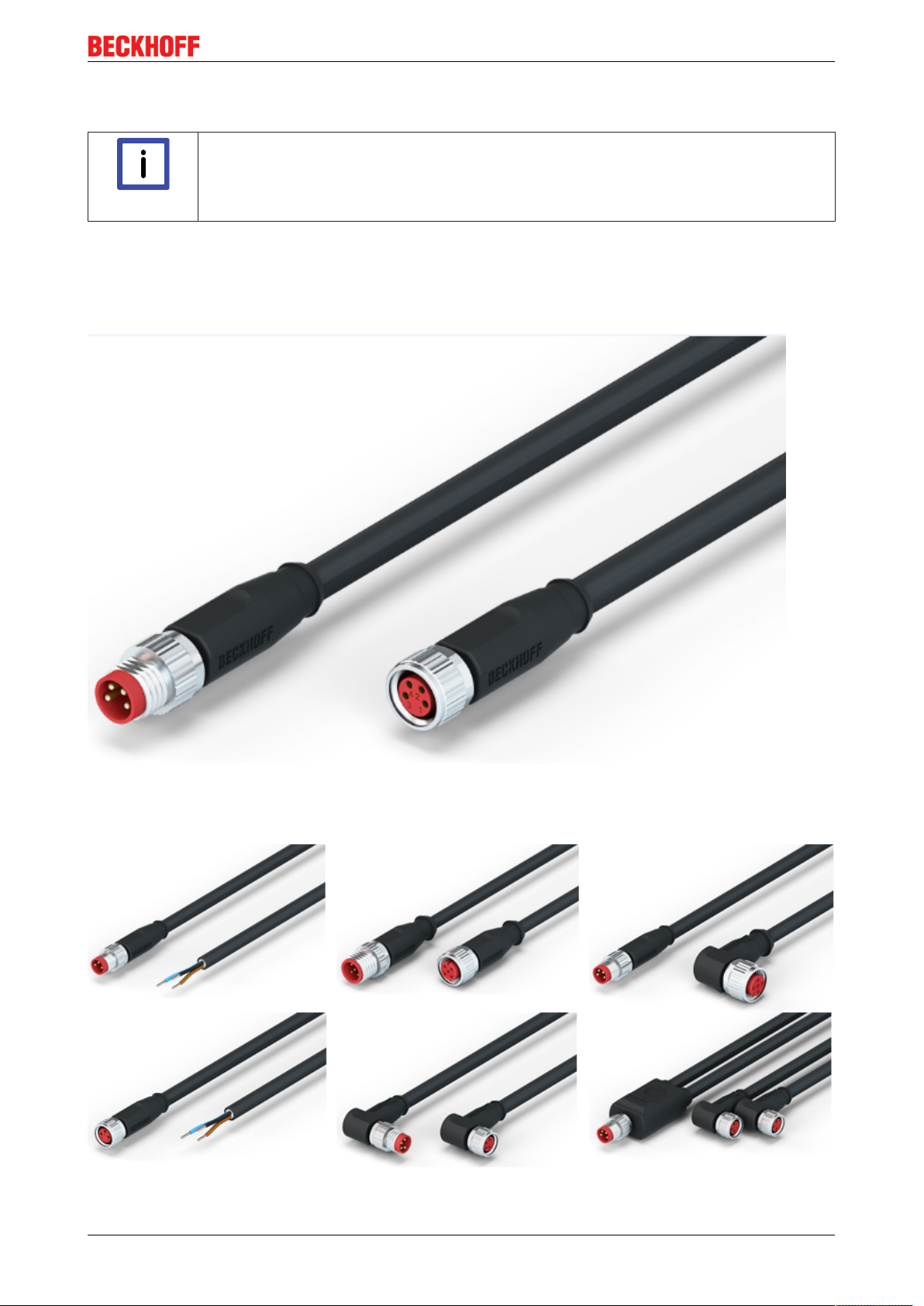
3.4 Cabling
A list of EtherCAT cables, power cables, sensor cables, Ethernet/EtherCAT connectors and fieldconfigurable connectors can be found under the following link: http://download.beckhoff.com/download/
document/catalog/main_catalog/german/Beckhoff_EtherCAT-Box-Zubehoer.pdf
The corresponding data sheets can be found under the following link:
https://beckhoff.de/default.asp?ethercat-box/ethercat_box_cables.htm?id=690338951657421
EtherCAT cables
Fig.22: ZK1090-3131-0xxx
EP9214-0023 and EP9224-002328 Version: 2.3.1
Page 29
Mounting and cabling
For connecting EtherCAT devices, only use shielded Ethernet cables with a minimum specification of
category5 (CAT5) according to EN50173 or ISO/IEC11801.
Wiring recommendations
Detailed recommendations for EtherCAT cabling can be found in the documentation "De-
Note
EtherCAT uses four cable wires for signal transmission.
Due to automatic cable detection (auto-crossing) symmetric (1:1) or cross-over cables can be used between
EtherCAT devices from Beckhoff.
Power cable
sign recommendations for EtherCAT/Ethernet infrastructure", which is available for download from www.beckhoff.de.
Fig.23: ZK2020-3132-0xxx
Sensor cables
Fig.24: Selection of Beckhoff sensor cables
EP9214-0023 and EP9224-0023 29Version: 2.3.1
Page 30
Mounting and cabling
3.5 Status LEDs and status bits
Below is a table showing the meaning of the status LEDs and status bits for the power outputs (EP9214 for
example):
Fig.25: EP9214 - status LEDs
Fig.26: EP9214 - status bits
Initialization
When switching on the voltage supply to the EP9214/ EP9224, all green LEDs and then all red LEDs are
switched on briefly to test the LEDs.
The LED is valid for both voltages and currents (Us and Up; OR).
LED Status
Us / Up
Off 0 0 0 The output is ready
Green 1 0 0 The output is just switching on
Green 1 0 0 The output is switched on. Normal operating status.
Flashing
green
Flashing
red
Red 0 0 1 The output has been deactivated and can be returned to a
1 1 0 The output is still operating, but will switch off if conditions
0 1 1 The output has been switched off. Switching on again is not
Warning Error
Us / Up
Description
remain unchanged (Warning Ux).
yet possible (waiting time of 20seconds)
normal state by a reset.
EP9214-0023 and EP9224-002330 Version: 2.3.1
Page 31

Mounting and cabling
3.6 Monitoring and reset contacts
The EP9214 has a monitoring contact (signal contact) and a reset contact. These contacts are fed out via an
M8 plug and an M8 socket.
The contacts of this M8 plug and M8 socket are wired together 1:1.
Fig.27: EP9214 - Monitoring and reset connectors
Pin assignment
Fig.28: EP9214 - Monitoring and reset contacts
Contact Meaning
Pin 1 and 3:
Monitoring
Pin 4: Reset all errors are reset by applying 24VDC to the Reset contact.
The contacts of the M8 plug connectors can conduct a maximum current of 4A.
Potential-free signalling contact (normally open contact), closes on application of the
supply voltage and if an error occurs in one of the eight load circuits
EP9214-0023 and EP9224-0023 31Version: 2.3.1
Page 32
Comissioning and Configuration
4 Comissioning and Configuration
4.1 Inserting into the EtherCAT network
Installation of the latest XML device description
Please ensure that you have installed the latest XML device description in TwinCAT. This
Note
At the Beckhoff TwinCAT System Manager the configuration tree can be build in two different ways:
• by scanning [}32] for existing hardware (called "online") and
• by manual inserting/appending [}32] of fieldbus devices, couplers and slaves.
Automatic scanning in of the box
• The EtherCAT system must be in a safe, de-energized state before the EtherCAT modules are
connected to the EtherCAT network!
• Switch on the operating voltage, open the TwinCAT System Manager [}35] (Config mode), and scan
in the devices (see Fig. 1). Acknowledge all dialogs with "OK", so that the configuration is in "FreeRun"
mode.
can be downloaded from the Beckhoff website (http://www.beckhoff.de/english/download/
elconfg.htm?id=1983920606140) and installed according to the installation instructions.
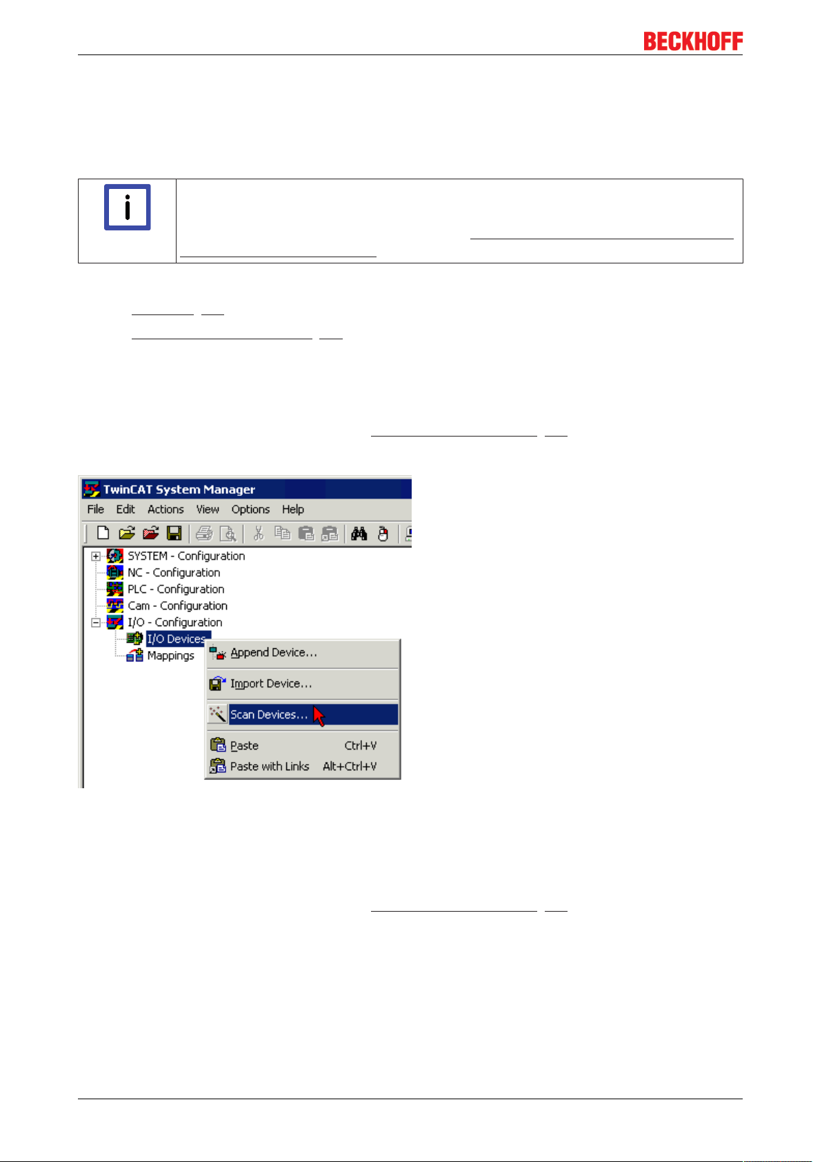
Fig.29: Scanning in the configuration (I/O Devices -> right-click -> Scan Devices...)
Appending a module manually
• The EtherCAT system must be in a safe, de-energized state before the EtherCAT modules are
connected to the EtherCAT network!
• Switch on the operating voltage, open the TwinCAT System Manager [}35] (Config mode)
• Append a new I/O device. In the dialog that appears select the device EtherCAT (Direct Mode), and
confirm with OK.
EP9214-0023 and EP9224-002332 Version: 2.3.1
Page 33

Comissioning and Configuration
Fig.30: Appending a new I/O device (I/O Devices -> right-click -> Append Device...)
Fig.31: Selecting the device EtherCAT
• Append a new box.
Fig.32: Appending a new box (Device -> right-click -> Append Box...)
• In the dialog that appears select the desired box (e.g. EP2816-0008), and confirm with OK.
EP9214-0023 and EP9224-0023 33Version: 2.3.1
Page 34

Comissioning and Configuration
Fig.33: Selecting a Box (e.g. EP2816-0008)
Fig.34: Appended Box in the TwinCAT tree
EP9214-0023 and EP9224-002334 Version: 2.3.1
Page 35
Comissioning and Configuration
4.2 Configuration via TwinCAT
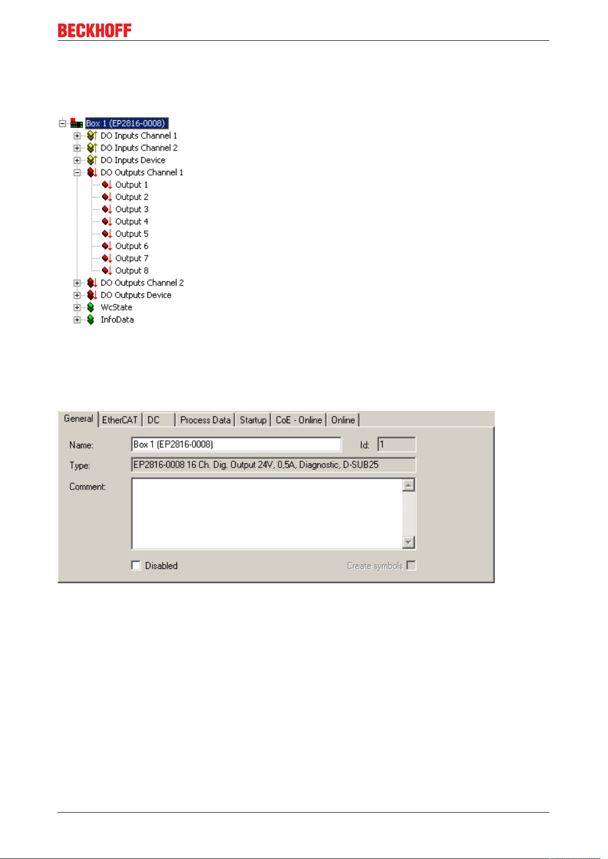
In the left-hand window of the TwinCAT System Manager, click on the branch of the EtherCAT Box you wish
to configure (EP2816-0008 in this example).
Fig.35: Branch of the EtherCAT box to be configured
In the right-hand window of the TwinCAT System manager, various tabs are now available for configuring
the EtherCAT Box.
General tab
Fig.36: General tab
Name Name of the EtherCAT device
Id Number of the EtherCAT device
Type EtherCAT device type
Comment Here you can add a comment (e.g. regarding the system).
Disabled Here you can deactivate the EtherCAT device.
Create symbols Access to this EtherCAT slave via ADS is only available if this checkbox is
activated.
EP9214-0023 and EP9224-0023 35Version: 2.3.1
Page 36

Comissioning and Configuration
EtherCAT tab
Fig.37: EtherCAT tab
Type EtherCAT device type
Product/Revision Product and revision number of the EtherCAT device
Auto Inc Addr. Auto increment address of the EtherCAT device. The auto increment address can
be used for addressing each EtherCAT device in the communication ring through
its physical position. Auto increment addressing is used during the start-up phase
when the EtherCAT master allocates addresses to the EtherCAT devices. With
auto increment addressing the first EtherCAT slave in the ring has the address
0000
. For each further slave the address is decremented by 1 (FFFF
hex
, FFFE
hex
etc.).
EtherCAT Addr. Fixed address of an EtherCAT slave. This address is allocated by the EtherCAT
master during the start-up phase. Tick the checkbox to the left of the input field in
order to modify the default value.
Previous Port Name and port of the EtherCAT device to which this device is connected. If it is
possible to connect this device with another one without changing the order of the
EtherCAT devices in the communication ring, then this combobox is activated and
the EtherCAT device to which this device is to be connected can be selected.
Advanced Settings This button opens the dialogs for advanced settings.
hex
The link at the bottom of the tab points to the product page for this EtherCAT device on the web.
Process Data tab
Indicates the configuration of the process data. The input and output data of the EtherCAT slave are
represented as CANopen process data objects (PDO). The user can select a PDO via PDO assignment and
modify the content of the individual PDO via this dialog, if the EtherCAT slave supports this function.
EP9214-0023 and EP9224-002336 Version: 2.3.1
Page 37

Comissioning and Configuration
Fig.38: Process Data tab
Sync Manager
Lists the configuration of the Sync Manager (SM).
If the EtherCAT device has a mailbox, SM0 is used for the mailbox output (MbxOut) and SM1 for the mailbox
input (MbxIn).
SM2 is used for the output process data (outputs) and SM3 (inputs) for the input process data.
If an input is selected, the corresponding PDO assignment is displayed in the PDO Assignment list below.
PDO Assignment
PDO assignment of the selected Sync Manager. All PDOs defined for this Sync Manager type are listed
here:
• If the output Sync Manager (outputs) is selected in the Sync Manager list, all RxPDOs are displayed.
• If the input Sync Manager (inputs) is selected in the Sync Manager list, all TxPDOs are displayed.
The selected entries are the PDOs involved in the process data transfer. In the tree diagram of the System
Manager these PDOs are displayed as variables of the EtherCAT device. The name of the variable is
identical to the Name parameter of the PDO, as displayed in the PDO list. If an entry in the PDO assignment
list is deactivated (not selected and greyed out), this indicates that the input is excluded from the PDO
assignment. In order to be able do select a greyed out PDO, the currently selected PDO has to be
deselected first.
EP9214-0023 and EP9224-0023 37Version: 2.3.1
Page 38

Comissioning and Configuration
Activation of PDO assignment
• the EtherCAT slave has to run through the PS status transition cycle (from pre-opera-
Note
PDO list
List of all PDOs supported by this EtherCAT device. The content of the selected PDOs is displayed in the
PDO Content list. The PDO configuration can be modified by double-clicking on an entry.
Column Description
Index PDO index.
Size Size of the PDO in bytes.
Name Name of the PDO.
If this PDO is assigned to a Sync Manager, it appears as a variable of the slave with this
parameter as the name.
Flags F Fixed content: The content of this PDO is fixed and cannot be changed by the System
Manager.
M Mandatory PDO. This PDO is mandatory and must therefore be assigned to a Sync Manager!
Consequently, this PDO cannot be deleted from the PDO Assignment list
SM Sync Manager to which this PDO is assigned. If this entry is empty, this PDO does not take part in
the process data traffic.
SU Sync unit to which this PDO is assigned.
tional to safe-operational) once (see Online tab [}41]),
• and the System Manager has to reload the EtherCAT slaves ( button)
PDO Content
Indicates the content of the PDO. If flag F (fixed content) of the PDO is not set the content can be modified.
Download
If the device is intelligent and has a mailbox, the configuration of the PDO and the PDO assignments can be
downloaded to the device. This is an optional feature that is not supported by all EtherCAT slaves.
PDO Assignment
If this check box is selected, the PDO assignment that is configured in the PDO Assignment list is
downloaded to the device on startup. The required commands to be sent to the device can be viewed in the
Startup [}38] tab.
PDO Configuration
If this check box is selected, the configuration of the respective PDOs (as shown in the PDO list and the
PDO Content display) is downloaded to the EtherCAT slave.
Startup tab
The Startup tab is displayed if the EtherCAT slave has a mailbox and supports the CANopen over EtherCAT
(CoE) or Servo drive over EtherCAT protocol. This tab indicates which download requests are sent to the
mailbox during startup. It is also possible to add new mailbox requests to the list display. The download
requests are sent to the slave in the same order as they are shown in the list.
EP9214-0023 and EP9224-002338 Version: 2.3.1
Page 39

Fig.39: Startup tab
Column Description
Transition Transition to which the request is sent. This can either be
• the transition from pre-operational to safe-operational (PS), or
• the transition from safe-operational to operational (SO).
If the transition is enclosed in "<>" (e.g. <PS>), the mailbox request is fixed and cannot be
modified or deleted by the user.
Protocol Type of mailbox protocol
Index Index of the object
Data Date on which this object is to be downloaded.
Comment Description of the request to be sent to the mailbox
Comissioning and Configuration
Move Up This button moves the selected request up by one position in the list.
Move Down This button moves the selected request down by one position in the list.
New This button adds a new mailbox download request to be sent during startup.
Delete This button deletes the selected entry.
Edit This button edits an existing request.
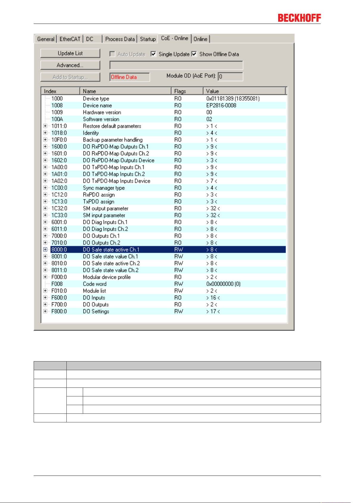
CoE - Online tab
The additional CoE - Online tab is displayed if the EtherCAT slave supports the CANopen over EtherCAT
(CoE) protocol. This dialog lists the content of the object directory of the slave (SDO upload) and enables the
user to modify the content of an object from this list. Details for the objects of the individual EtherCAT
devices can be found in the device-specific object descriptions.
EP9214-0023 and EP9224-0023 39Version: 2.3.1
Page 40
Comissioning and Configuration
Fig.40: CoE - Online tab
Object list display
Column Description
Index Index and subindex of the object
Name Name of the object
Flags RW The object can be read, and data can be written to the object (read/write)
RO The object can be read, but no data can be written to the object (read only)
P An additional P identifies the object as a process data object.
Value Value of the object
Update List The Update list button updates all objects in the displayed list
Auto Update If this check box is selected, the content of the objects is updated automatically.
Advanced The Advanced button opens the Advanced Settings dialog. Here you can specify which
objects are displayed in the list.
EP9214-0023 and EP9224-002340 Version: 2.3.1
Page 41

Comissioning and Configuration
Fig.41: Advanced settings
Online
- via SDO information
Offline
- via EDS file
Online tab
If this option button is selected, the list of the objects included in the object
directory of the slave is uploaded from the slave via SDO information. The list
below can be used to specify which object types are to be uploaded.
If this option button is selected, the list of the objects included in the object
directory is read from an EDS file provided by the user.
Fig.42: Online tab
EP9214-0023 and EP9224-0023 41Version: 2.3.1
Page 42

Comissioning and Configuration
State Machine
Init This button attempts to set the EtherCAT device to the Init state.
Pre-Op This button attempts to set the EtherCAT device to the pre-operational state.
Op This button attempts to set the EtherCAT device to the operational state.
Bootstrap This button attempts to set the EtherCAT device to the Bootstrap state.
Safe-Op This button attempts to set the EtherCAT device to the safe-operational state.
Clear Error This button attempts to delete the fault display. If an EtherCAT slave fails during
change of state it sets an error flag.
Example: An EtherCAT slave is in PREOP state (pre-operational). The master now
requests the SAFEOP state (safe-operational). If the slave fails during change of
state it sets the error flag. The current state is now displayed as ERR PREOP. When
the Clear Error button is pressed the error flag is cleared, and the current state is
displayed as PREOP again.
Current State Indicates the current state of the EtherCAT device.
Requested State Indicates the state requested for the EtherCAT device.
DLL Status
Indicates the DLL status (data link layer status) of the individual ports of the EtherCAT slave. The DLL status
can have four different states:
Status Description
No Carrier / Open No carrier signal is available at the port, but the port is open.
No Carrier / Closed No carrier signal is available at the port, and the port is closed.
Carrier / Open A carrier signal is available at the port, and the port is open.
Carrier / Closed A carrier signal is available at the port, but the port is closed.
File Access over EtherCAT
Download With this button a file can be written to the EtherCAT device.
Upload With this button a file can be read from the EtherCAT device.
EP9214-0023 and EP9224-002342 Version: 2.3.1
Page 43

Comissioning and Configuration
4.3 Operation with or without EtherCAT master
The EP92x4 is preset in the factory and delivered with a set rated current of 4.0A and all eight channels
switched on.
The channels switch on automatically during commissioning
In the basic setting the rated current of the EP92x4 is 4A per channel. Shortly after the
Attention
This is preset by the CoE object 0xF707:01
EP92x4 is supplied with voltage, all channels are switched on with a delay of 100ms each.
Fig.43: CoE object 0xF707:01 - Enable Control via Fieldbus
If the EP92x4 is operated on an EtherCAT master, the basic setting or the bootup can be adapted.
This is done via the variable DPO Outputs Device -> Enable control via Fieldbus in the process data.
At the next power-on of the box the load circuits will then be switched on depending on the settings in the
CoE objects.
Customize all parameters when EtherCAT is used for the first time
If the EP92x4 operated for the first time with EtherCAT connection, all parameters need to
Note
be adjusted.
Without EtherCAT connection the outputs switch in default status
After the EP92x4 was configured with an EtherCAT master you can disconnect the Ether-
Attention
Example for parametrizing the outputs when using EtherCAT
Via the tab “CoE – Online” you can adjust different settings of the box module. For example, it is possible to
adjust the “Nominal Current US” (Index: 8000:12), by double-clicking to the respective parameter opens the
“Set Value Dialog” (see following figure).
CAT connection. But in this case the parameters of all outputs switch in the default status.
When the connection is restored to the EtherCAT master, the previously set values are
available again.
EP9214-0023 and EP9224-0023 43Version: 2.3.1
Page 44

Comissioning and Configuration
Fig.44: Adjust the “DPO Settings Ch.1” with EtherCAT connection
If the EtherCAT connection is disconnected, the option “Show Offline Data” should be activated. Then the
default values of the parameters are displayed.
4.4 Switch of behavior
4.4.1 Switch-off characteristics
The EP9214 EtherCAT Box selectively protects all connected 24VDC load circuits. This is done via various
electronic circuits, additionally protected by a 7A micro-fuse.
Selective switch-off means that the load circuits are individually monitored and if a channel is exceeded, only
that channel is switched off.
This ensures the function of the remaining consumers connected to the higher-level power supply unit.
General functional principle
The EP9214 EtherCAT Box monitors the current for each of the 8 output channels. 4xUs, 4xUp. Switching
off takes place depending on the selected nominal current and release characteristic.
Superordinate to all is the hardware switch-off, which responds if
• 7A is reached for 50ms
• there is a short-circuit for 50ms
• the capacitive load and thus the start-up current of the connected devices is too high
Due to the intelligent current limitation an output current exceeding 7A is not possible under operating
conditions. The additionally installed 7A micro fuse thus blows only if the upstream electronic switch-off is
already defective.
The nominal current can be set for each channel individually between 1A and 4A.
EP9214-0023 and EP9224-002344 Version: 2.3.1
Page 45
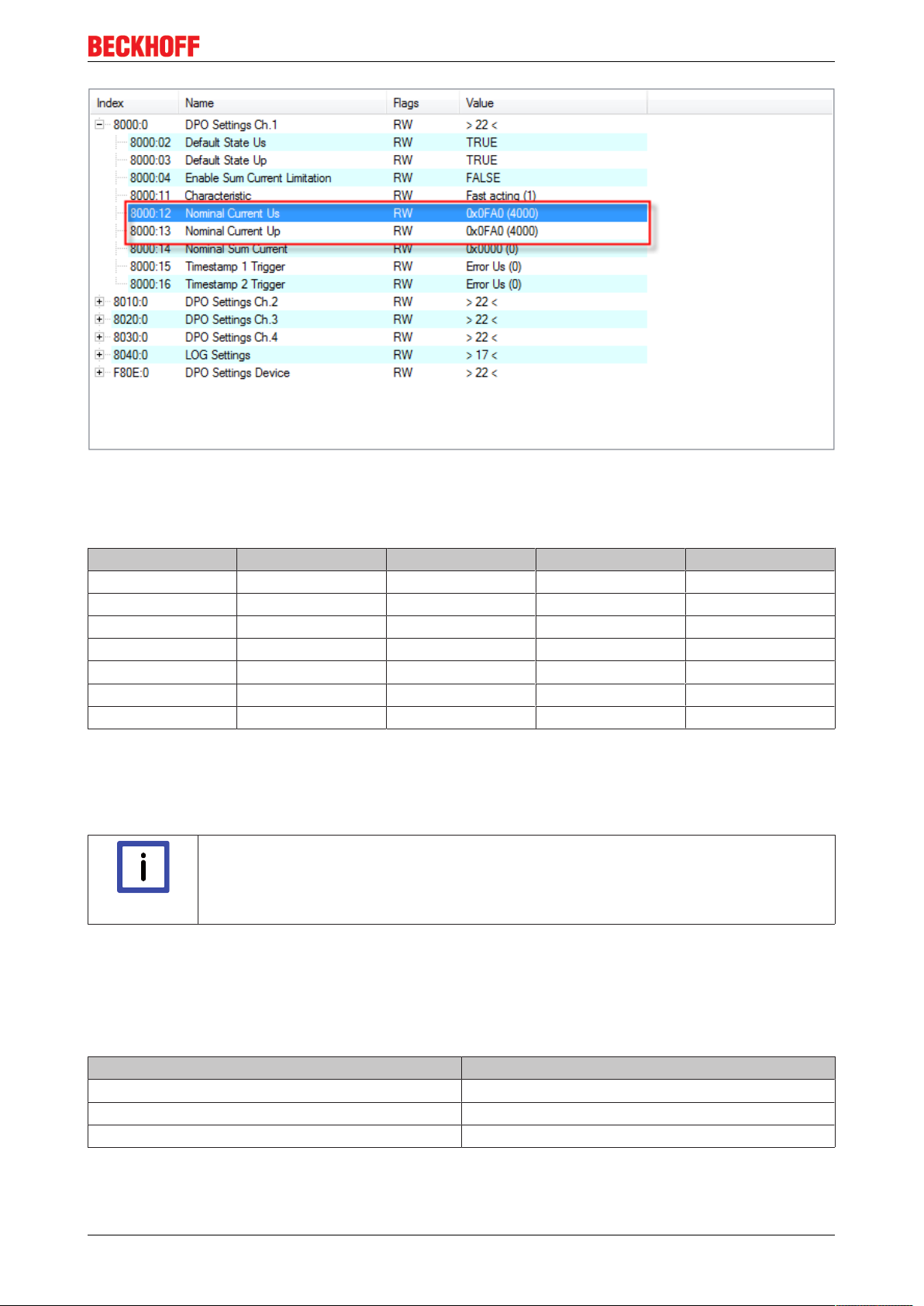
Fig.45: Setting the nominal current
Comissioning and Configuration
All set characteristics are referenced to the set nominal current. The following table shows the response time
of the monitoring in relation to the nominal current and characteristic.
Nominal current Very fast acting Fast acting Slow acting Time delay
100% 1h - - 110% 1h 4h - 120% 7min 4h - 150% 30s 30min 1h 4h
210% 500ms 20s 20s 100s
275% 500ms 1s 20s 10s
300% 20ms 100ms 1s 3s
If overcurrent (≥ nominal current) is detected and it is foreseeable that the current monitoring will trip if
conditions remain unchanged, then a warning is given both in the process data and in form of a flashing
LED. An output switch-off due to overcurrent is indicated by a red LED.
If one of the outputs was switched off due to a diagnosis, it must be reactivated by an active RESET.
Restart after power OFF/ON
If an output was switched off due to an error, then an active reset by the RESET contact or
Note
Switching on can be done either via EtherCAT or by applying 24V to the RESET contact. To protect the
circuitry, a RESET can take place maximally every 20seconds. Faster successive edges are ignored.
the fieldbus is necessary. Switching off and on again is not sufficient! To protect the electronic a RESET can be done at maximum all 20seconds.
Switch-on delay of load circuits 1 to 4 without fieldbus control
Here is a table of the startup times, adjustable in the CoE object 0xF80E:11
Description Switch-on delay
Fast 10ms
Moderate 100ms
Slow 200ms
EP9214-0023 and EP9224-0023 45Version: 2.3.1
Page 46
Comissioning and Configuration
4.4.2 Current limitation, switching the load circuits off
The switch-off behavior of the individual load circuits can be adapted to the application.
The following modes can be set individually for each channel:
• Very fast acting
• Fast acting
• Slow acting
• Time delay
Release time (switch-off time) of the modes
Rated current Very fast acting Fast acting Slow acting Time delay
100% 1h - - 110% 1h 4h - 120% 7min 4 h - 150% 30s 30min 1h 4h
210% 500ms 20sec 20s 100s
275% 500ms 1sec 20s 10s
300% 20ms 100ms 1s 3s
The release time depends on the set rated current.
Following the switch-off of a channel it is necessary to reactivate it after rectification of the cause of the error.
Switch-off of the box due to overtemperature
The EP9214 is internally protected against overheating. A warning is given in the process data if a
temperature of about 80°C is reached.
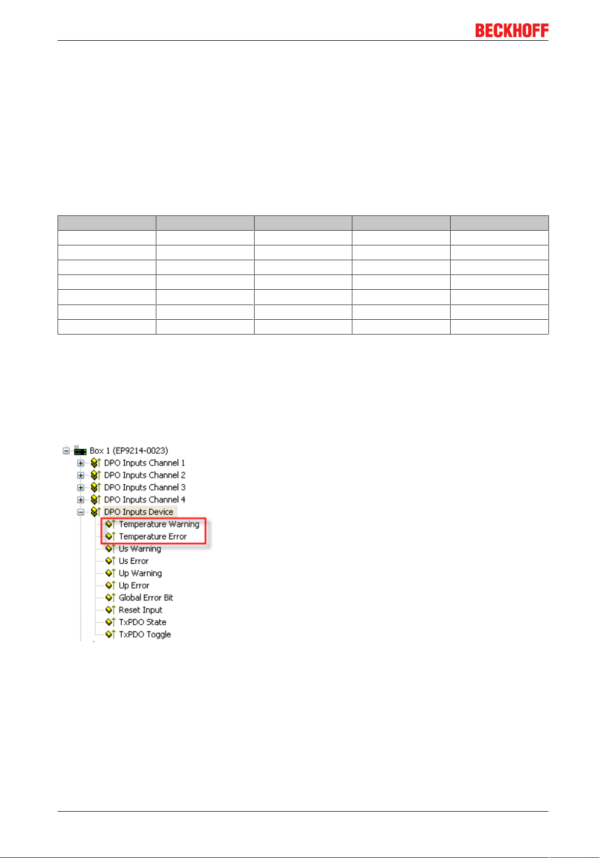
Fig.46: Temperature Warning and Temperature Error bits
On reaching 85°C all load circuits are switched off in order to protect the hardware against destruction. In
this case the Temperature Error bit is set.
So that the permitted temperature is not exceeded, the box is to be mounted with its rear wall on the flattest
possible thermally conductive surface.
Switch off of the box due to undervoltage
Since undervoltage impairs the function of the safety mechanisms, a warning is given in the process data
from an input voltage of 21.5V. If the voltage falls below 18V all outputs are switched off and the Error bit is
set.
EP9214-0023 and EP9224-002346 Version: 2.3.1
Page 47
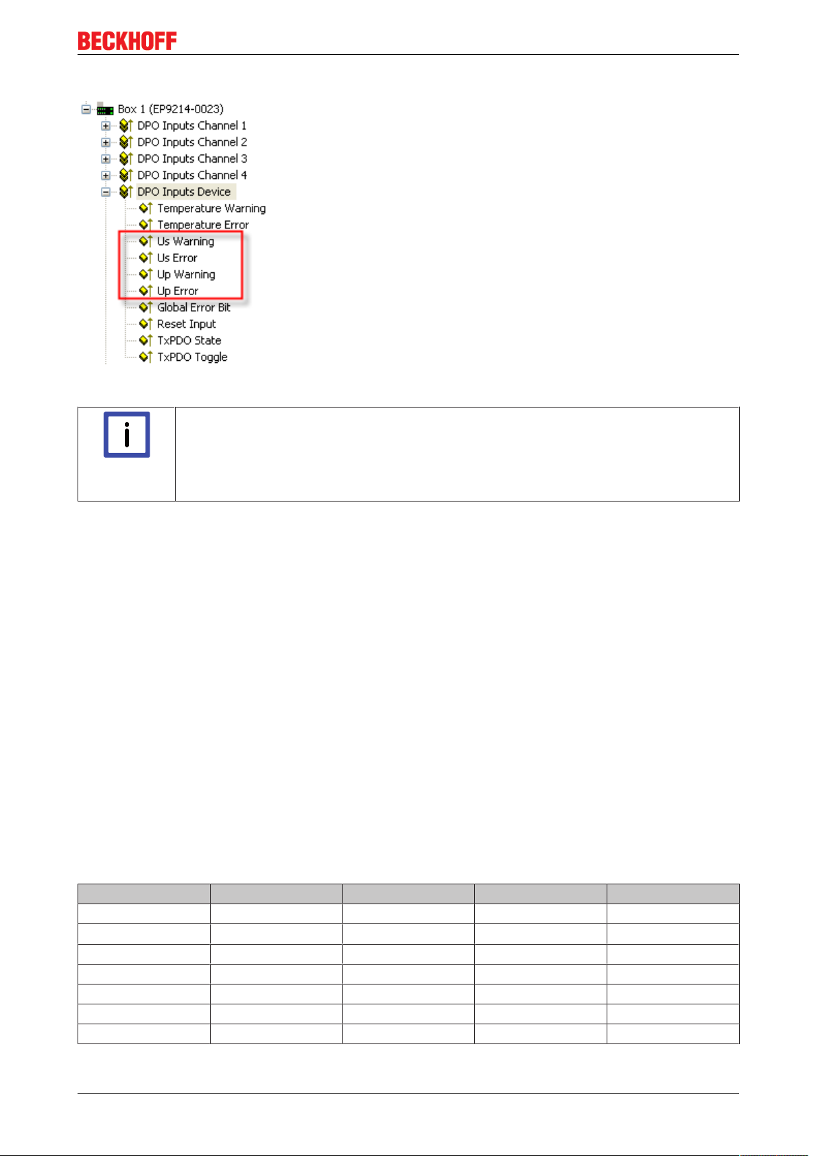
Undervoltage is detected independently for Us and Up.
Fig.47: Undervoltage bits
Switching on again
Switching off due to undervoltage and overtemperature is equivalent to the response of the
Note
current monitoring, but applies to the entire box and all outputs. The error must be reset by
setting the process data GLOBAL RESET or by power off/ restart of the module, furthermore the temperature must have fallen below 75°C!
Comissioning and Configuration
Switching load circuits on again after switch-off
This takes place either via the process data by EtherCAT or by the reset input directly on the box.
Also see about this
2 EP9214-0023 - Process image [}65]
2 Monitoring and reset contacts [}31]
4.4.3 Setting the current limitation
The switch-off behavior of the individual load circuits can be adapted to the application.
The following modes can be set individually for each channel:
• Very fast acting
• Fast acting
• Slow acting
• Time delay
Release time (switch-off time) of the modes
Rated current Very fast acting Fast acting Slow acting Time delay
100% 1h - - 110% 1h 4h - 120% 7min 4 h - 150% 30s 30min 1h 4h
210% 500ms 20sec 20s 100s
275% 500ms 1sec 20s 10s
300% 20ms 100ms 1s 3s
EP9214-0023 and EP9224-0023 47Version: 2.3.1
Page 48

Comissioning and Configuration
The release time depends on the set rated current.
CoE parameters for setting the current limiting characteristic
Fig.48: CoE parameters for setting the current limiting characteristic
Meaning of the parameters
Index Name Meaning
0x80n0:02 Default State Us TRUE: in case of operation without fieldbus the load circuit Us of
channel n is automatically switched on
FALSE: in case of operation without fieldbus the load circuit Us of
channel n remains switched off
0x80n0:02 Default State Up TRUE: in case of operation without fieldbus the load circuit Up of
channel n is automatically switched on
FALSE: in case of operation without fieldbus the load circuit Up of
channel n remains switched off
0x80n0:11 Characteristic Release time depending on rated current
0x80n0:12 Nominal Current Us Specification of the rated current of Us in mA
0x80n0:13 Nominal Current Up Specification of the rated current of Up in mA
Switching load circuits on again after switch-off
This takes place either via the process data [}65] by EtherCAT or by the reset input [}31] directly on the
box.
4.4.4 Status LEDs and status bits
Below is a table showing the meaning of the status LEDs and status bits for the power outputs (EP9214 for
example):
EP9214-0023 and EP9224-002348 Version: 2.3.1
Page 49

Fig.49: EP9214 - Status bits
Comissioning and Configuration
Fig.50: EP9214 - status bits
Initialization
When switching on the voltage supply to the EP9214/EP9224, all green LEDs and then all red LEDs are
switched on briefly to test the LEDs.
The LED is valid for both voltages and currents (Us and Up; OR).
LED Status
Us / Up
Off 0 0 0 The output is ready
Green 1 0 0 The output is just switching on
Green 1 0 0 The output is switched on. Normal operating
Flashing green 1 1 0 The output is still operating, but will switch off if
Flashing red 0 1 1 The output has been switched off. Switching on
Red 0 0 1 The output has been deactivated and can be
Warning Error
Us / Up
Description
status.
conditions remain unchanged (Warning Ux).
again is not yet possible (waiting time of
20seconds)
returned to a normal state by a reset.
EP9214-0023 and EP9224-0023 49Version: 2.3.1
Page 50

Comissioning and Configuration
4.5 EP9214-0023
4.5.1 EP9214-0023 - Object description
Parameterization
Terminals' parameterization will be conducted by the CoE tab (double-click on the referring
Note
Note
The CoE overview contains objects for different intended applications:
• Objects required for parameterization during commissioning
• Objects intended for regular operation e.g. through ADS access
• Objects for indicating internal settings (may be fixed)
• Further profile-specific objects indicating inputs, outputs and status information
object) or the Process data tab (PDO assignment)
EtherCAT XML Device Description
The description correspond to the display of the CoE objects from the EtherCAT XML Device Description. It is strongly recommended to download the latest revision of the corresponding XML file from the Beckhoff website (http://www.beckhoff.com/english/default.htm?
download/elconfg.htm) and follow the installation instructions.
The following section first describes the objects require for normal operation, followed by a complete
overview of missing objects.
4.5.1.1 Objects for parameterization
4.5.1.1.1 Index 1011 Restore default parameters
Index Name Meaning Data type Flags Default
1011:0 Restore default
parameters
1011:01 SubIndex 001 If this object is set to "0x64616F6C" in the set value dialog,
4.5.1.1.2 Index 8000 DPO Settings Ch.1
Index Name Meaning Data type Flags Default
8010:0 DPO Settings
Ch.1
8010:02 Default State Us The output adopts this value if F707:01 is not set boolean RW 0x01 (1
8010:03 Default State Up The output adopts this value if F707:01 is not set boolean RW 0x01 (1
8010:11 Characteristic Specifies the characteristic with which the current monitor-
8010:12 Nominal CurrentUsNominal maximum current at the output UINT16 RW 0x0FA0 (4000
Making default settings UINT8 RO 0x01 (1
all backup objects are reset to their delivery state.
ing reacts:
0
: very fast acting
dec
1
: fast acting
dec
2
: slow acting
dec
3
: time delay
dec
UINT32 RW 0x00000000 (0
UINT8 RO 0x13 (19
UINT16 RW 0x0001 (1
)
dec
)
dec
)
dec
)
dec
dec
)
dec
)
)
dec
8010:13 Nominal CurrentUpNominal maximum current at the output UINT16 RW 0x0FA0 (4000
EP9214-0023 and EP9224-002350 Version: 2.3.1
)
dec
Page 51

Comissioning and Configuration
4.5.1.1.3 Index 8010 DPO Settings Ch.2
Index Name Meaning Data type Flags Default
8010:0 DPO Settings
Ch.2
8010:02 Default State Us The output adopts this value if F707:01 is not set boolean RW 0x01 (1
8010:03 Default State Up The output adopts this value if F707:01 is not set boolean RW 0x01 (1
8010:11 Characteristic Specifies the characteristic with which the current monitor-
ing reacts:
0
: very fast acting
dec
1
: fast acting
dec
2
: slow acting
dec
3
: time delay
dec
8010:12 Nominal CurrentUsNominal maximum current at the output UINT16 RW 0x0FA0 (4000
UINT8 RO 0x13 (19
dec
dec
UINT16 RW 0x0001 (1
)
dec
)
)
dec
)
)
dec
8010:13 Nominal CurrentUpNominal maximum current at the output UINT16 RW 0x0FA0 (4000
4.5.1.1.4 Index 8020 DPO Settings Ch.3
Index Name Meaning Data type Flags Default
8020:0 DPO Settings
Ch.3
8020:02 Default State Us The output adopts this value if F707:01 is not set boolean RW 0x01 (1
8020:03 Default State Up The output adopts this value if F707:01 is not set boolean RW 0x01 (1
8020:11 Characteristic Specifies the characteristic with which the current monitor-
ing reacts:
0
: very fast acting
dec
1
: fast acting
dec
2
: slow acting
dec
3
: time delay
dec
UINT8 RO 0x13 (19
dec
dec
UINT16 RW 0x0001 (1
)
dec
)
)
dec
8020:12 Nominal CurrentUsNominal maximum current at the output UINT16 RW 0x0FA0 (4000
8020:13 Nominal CurrentUpNominal maximum current at the output UINT16 RW 0x0FA0 (4000
4.5.1.1.5 Index 8030 DPO Settings Ch.4
Index Name Meaning Data type Flags Default
8030:0 DPO Settings
Ch.4
8030:02 Default State Us The output adopts this value if F707:01 is not set boolean RW 0x01 (1
8030:03 Default State Up The output adopts this value if F707:01 is not set boolean RW 0x01 (1
8030:11 Characteristic Specifies the characteristic with which the current monitor-
ing reacts:
0
: very fast acting
dec
1
: fast acting
dec
2
: slow acting
dec
3
: time delay
dec
8030:12 Nominal CurrentUsNominal maximum current at the output UINT16 RW 0x0FA0 (4000
UINT8 RO 0x13 (19
dec
dec
UINT16 RW 0x0001 (1
)
dec
)
)
dec
)
dec
)
)
dec
)
dec
)
)
dec
8030:13 Nominal CurrentUpNominal maximum current at the output UINT16 RW 0x0FA0 (4000
4.5.1.1.6 Index F707 DPO Outputs Device
Index Name Meaning Data type Flags Default
F707:0 DPO Outputs
Device
F707:01 Enable Control
Via Fieldbus
0
: All outputs are set to their default values (80X0:02,
bin
80X0:03)
1
: All outputs are set according to their PDOs (70X0:01,
bin
70X0:02)
F707:04 Global Reset All error bits are reset boolean RO 0x00 (0
UINT8 RO 0x04 (4
boolean RO 0x00 (0
)
dec
)
dec
)
dec
EP9214-0023 and EP9224-0023 51Version: 2.3.1
)
dec
Page 52

Comissioning and Configuration
4.5.1.1.7 Index F80E DPO Settings Device
Index Name Meaning Data type Flags Default
F80E:0 DPO Settings
UINT8 RO 0x11 (17
Device
F80E:11 Startup Delay Sets the time that is kept between two switch-on proce-
UINT16 RW 0x0001 (1
dures:
1
: fast (10ms)
dec
2
: moderate (100ms)
dec
3
: slow (200ms)
dec
4.5.1.2 Standard objects
The standard objects have the same meaning for all EtherCAT slaves.
4.5.1.2.1 Index 1000 Device type
Index Name Meaning Data type Flags Default
1000:0 Device type Device type of the EtherCAT slave: The low word contains
the CoE profile used (5001). The high word contains the
module profile according to the modular device profile.
UINT32 RO 0x010E1389
(17699721
)
dec
)
dec
)
dec
4.5.1.2.2 Index 1008 Device name
Index Name Meaning Data type Flags Default
1008:0 Device name Device name of the EtherCAT slave STRING RO EP9214-0023
4.5.1.2.3 Index 1009 Hardware version
Index Name Meaning Data type Flags Default
1009:0 Hardware ver-
Hardware version of the EtherCAT slave STRING RO
sion
4.5.1.2.4 Index 100A Software version
Index Name Meaning Data type Flags Default
100A:0 Software ver-
Firmware version of the EtherCAT slave STRING RO 06
sion
4.5.1.2.5 Index 1018 Identity
Index Name Meaning Data type Flags Default
1018:0 Identity Information for identifying the slave UINT8 RO 0x04 (4
1018:01 Vendor ID Vendor ID of the EtherCAT slave UINT32 RO 0x00000002 (2
1018:02 Product code Product code of the EtherCAT slave UINT32 RO 0x23FE4052
(603865170
1018:03 Revision Revision numberof the EtherCAT slave; the low word (bit
UINT32 RO 0x00000000 (0
0-15) indicates the special terminal number, the high word
(bit 16-31) refers to the device description
1018:04 Serial number Serial number of the EtherCAT slave; the low byte (bit 0-7)
UINT32 RO 0x00000000 (0
of the low word contains the year of production, the high
byte (bit 8-15) of the low word contains the week of production, the high word (bit 16-31) is 0
)
dec
dec
)
dec
)
)
dec
)
dec
EP9214-0023 and EP9224-002352 Version: 2.3.1
Page 53

Comissioning and Configuration
4.5.1.2.6 Index 10F0 Backup parameter handling
Index Name Meaning Data type Flags Default
10F0:0 Backup parame-
ter handling
Information for standardized loading and saving of backup
entries
UINT8 RO 0x01 (1
)
dec
10F0:01 Checksum Checksum across all backup entries of the EtherCAT slave UINT32 RO 0x00000000 (0
4.5.1.2.7 Index 1600 DPO RxPDO-Map Outputs Ch.1
Index Name Meaning Data type Flags Default
1600:0 DPO RxPDO-
Map Outputs
Ch.1
1600:01 SubIndex 001 1. PDO Mapping entry (object 0x7000 (DPO Outputs Ch.1),
1600:02 SubIndex 002 2. PDO Mapping entry (object 0x7000 (DPO Outputs Ch.1),
1600:03 SubIndex 003 3. PDO Mapping entry (2 bits align) UINT32 RO 0x0000:00, 2
1600:04 SubIndex 004 4. PDO Mapping entry (object 0x7000 (DPO Outputs Ch.1),
1600:05 SubIndex 005 5. PDO Mapping entry (object 0x7000 (DPO Outputs Ch.1),
1600:06 SubIndex 006 6. PDO Mapping entry (10 bits align) UINT32 RO 0x0000:00, 10
PDO Mapping RxPDO 1 UINT8 RO 0x06 (6
UINT32 RO 0x7000:01, 1
entry 0x01 (Output Us))
UINT32 RO 0x7000:02, 1
entry 0x02 (Output Up))
UINT32 RO 0x7000:05, 1
entry 0x05 (Reset Us))
UINT32 RO 0x7000:06, 1
entry 0x06 (Reset Up))
)
dec
)
dec
4.5.1.2.8 Index 1601 DPO RxPDO-Map Outputs Ch.2
Index Name Meaning Data type Flags Default
1601:0 DPO RxPDO-
Map Outputs
PDO Mapping RxPDO 2 UINT8 RO 0x06 (6
)
dec
Ch.2
1601:01 SubIndex 001 1. PDO Mapping entry (object 0x7010 (DPO Outputs Ch.2),
UINT32 RO 0x7010:01, 1
entry 0x01 (Output Us))
1601:02 SubIndex 002 2. PDO Mapping entry (object 0x7010 (DPO Outputs Ch.2),
UINT32 RO 0x7010:02, 1
entry 0x02 (Output Up))
1601:03 SubIndex 003 3. PDO Mapping entry (2 bits align) UINT32 RO 0x0000:00, 2
1601:04 SubIndex 004 4. PDO Mapping entry (object 0x7010 (DPO Outputs Ch.2),
UINT32 RO 0x7010:05, 1
entry 0x05 (Reset Us))
1601:05 SubIndex 005 5. PDO Mapping entry (object 0x7010 (DPO Outputs Ch.2),
UINT32 RO 0x7010:06, 1
entry 0x06 (Reset Up))
1601:06 SubIndex 006 6. PDO Mapping entry (10 bits align) UINT32 RO 0x0000:00, 10
4.5.1.2.9 Index 1602 DPO RxPDO-Map Outputs Ch.3
Index Name Meaning Data type Flags Default
1602:0 DPO RxPDO-
Map Outputs
Ch.3
1602:01 SubIndex 001 1. PDO Mapping entry (object 0x7020 (DPO Outputs Ch.3),
1602:02 SubIndex 002 2. PDO Mapping entry (object 0x7020 (DPO Outputs Ch.3),
1602:03 SubIndex 003 3. PDO Mapping entry (2 bits align) UINT32 RO 0x0000:00, 2
1602:04 SubIndex 004 4. PDO Mapping entry (object 0x7020 (DPO Outputs Ch.3),
1602:05 SubIndex 005 5. PDO Mapping entry (object 0x7020 (DPO Outputs Ch.3),
1602:06 SubIndex 006 6. PDO Mapping entry (10 bits align) UINT32 RO 0x0000:00, 10
PDO Mapping RxPDO 3 UINT8 RO 0x06 (6
UINT32 RO 0x7020:01, 1
entry 0x01 (Output Us))
UINT32 RO 0x7020:02, 1
entry 0x02 (Output Up))
UINT32 RO 0x7020:05, 1
entry 0x05 (Reset Us))
UINT32 RO 0x7020:06, 1
entry 0x06 (Reset Up))
)
dec
EP9214-0023 and EP9224-0023 53Version: 2.3.1
Page 54

Comissioning and Configuration
4.5.1.2.10 Index 1603 DPO RxPDO-Map Outputs Ch.4
Index Name Meaning Data type Flags Default
1603:0 DPO RxPDO-
Map Outputs
PDO Mapping RxPDO 4 UINT8 RO 0x06 (6
)
dec
Ch.4
1603:01 SubIndex 001 1. PDO Mapping entry (object 0x7030 (DPO Outputs Ch.4),
UINT32 RO 0x7030:01, 1
entry 0x01 (Output Us))
1603:02 SubIndex 002 2. PDO Mapping entry (object 0x7030 (DPO Outputs Ch.4),
UINT32 RO 0x7030:02, 1
entry 0x02 (Output Up))
1603:03 SubIndex 003 3. PDO Mapping entry (2 bits align) UINT32 RO 0x0000:00, 2
1603:04 SubIndex 004 4. PDO Mapping entry (object 0x7030 (DPO Outputs Ch.4),
UINT32 RO 0x7030:05, 1
entry 0x05 (Reset Us))
1603:05 SubIndex 005 5. PDO Mapping entry (object 0x7030 (DPO Outputs Ch.4),
UINT32 RO 0x7030:06, 1
entry 0x06 (Reset Up))
1603:06 SubIndex 006 6. PDO Mapping entry (10 bits align) UINT32 RO 0x0000:00, 10
4.5.1.2.11 Index 1604 DPO RxPDO-Map Outputs Device
Index Name Meaning Data type Flags Default
1604:0 DPO RxPDO-
Map Outputs
Device
1604:01 SubIndex 001 1. PDO Mapping entry (object 0xF707 (DPO Outputs De-
1604:02 SubIndex 002 2. PDO Mapping entry (2 bits align) UINT32 RO 0x0000:00, 2
1604:03 SubIndex 003 3. PDO Mapping entry (object 0xF707 (DPO Outputs De-
1604:04 SubIndex 004 4. PDO Mapping entry (12 bits align) UINT32 RO 0x0000:00, 12
PDO Mapping RxPDO 5 UINT8 RO 0x04 (4
UINT32 RO 0xF707:01, 1
vice), entry 0x01 (Enable Control Via Fieldbus))
UINT32 RO 0xF707:04, 1
vice), entry 0x04 (Global Reset))
)
dec
4.5.1.2.12 Index 1A00 DPO TxPDO-Map Inputs Ch.1
Index Name Meaning Data type Flags Default
1A00:0 DPO TxPDO-
Map Inputs Ch.1
1A00:01 SubIndex 001 1. PDO Mapping entry (object 0x6000 (DPO Inputs Ch.1),
1A00:02 SubIndex 002 2. PDO Mapping entry (object 0x6000 (DPO Inputs Ch.1),
1A00:03 SubIndex 003 3. PDO Mapping entry (object 0x6000 (DPO Inputs Ch.1),
1A00:04 SubIndex 004 4. PDO Mapping entry (object 0x6000 (DPO Inputs Ch.1),
1A00:05 SubIndex 005 5. PDO Mapping entry (object 0x6000 (DPO Inputs Ch.1),
1A00:06 SubIndex 006 6. PDO Mapping entry (object 0x6000 (DPO Inputs Ch.1),
1A00:07 SubIndex 007 7. PDO Mapping entry (object 0x6000 (DPO Inputs Ch.1),
1A00:08 SubIndex 008 8. PDO Mapping entry (6 bits align) UINT32 RO 0x0000:00, 6
1A00:09 SubIndex 009 9. PDO Mapping entry (object 0x6000 (DPO Inputs Ch.1),
1A00:0A SubIndex 010 10. PDO Mapping entry (object 0x6000 (DPO Inputs Ch.1),
1A00:0B SubIndex 011 11. PDO Mapping entry (object 0x6000 (DPO Inputs Ch.1),
PDO Mapping TxPDO 1 UINT8 RO 0x0B (11
UINT32 RO 0x6000:01, 1
entry 0x01 (Error Us))
UINT32 RO 0x6000:02, 1
entry 0x02 (Error Up))
UINT32 RO 0x6000:03, 1
entry 0x03 (Warning Us))
UINT32 RO 0x6000:04, 1
entry 0x04 (Warning Up))
UINT32 RO 0x6000:05, 1
entry 0x05 (Status Us))
UINT32 RO 0x6000:06, 1
entry 0x06 (Status Up))
UINT32 RO 0x6000:07, 1
entry 0x07 (Channel Error))
UINT32 RO 0x6000:0E, 1
entry 0x0E (Sync error))
UINT32 RO 0x6000:0F, 1
entry 0x0F (TxPDO State))
UINT32 RO 0x6000:10, 1
entry 0x10 (TxPDO Toggle))
dec
)
EP9214-0023 and EP9224-002354 Version: 2.3.1
Page 55

Comissioning and Configuration
4.5.1.2.13 Index 1A01 DPO TxPDO-Map Inputs Ch.2
Index Name Meaning Data type Flags Default
1A01:0 DPO TxPDO-
Map Inputs Ch.2
1A01:01 SubIndex 001 1. PDO Mapping entry (object 0x6010 (DPO Inputs Ch.2),
1A01:02 SubIndex 002 2. PDO Mapping entry (object 0x6010 (DPO Inputs Ch.2),
1A01:03 SubIndex 003 3. PDO Mapping entry (object 0x6010 (DPO Inputs Ch.2),
1A01:04 SubIndex 004 4. PDO Mapping entry (object 0x6010 (DPO Inputs Ch.2),
1A01:05 SubIndex 005 5. PDO Mapping entry (object 0x6010 (DPO Inputs Ch.2),
1A01:06 SubIndex 006 6. PDO Mapping entry (object 0x6010 (DPO Inputs Ch.2),
1A01:07 SubIndex 007 7. PDO Mapping entry (object 0x6010 (DPO Inputs Ch.2),
1A01:08 SubIndex 008 8. PDO Mapping entry (6 bits align) UINT32 RO 0x0000:00, 6
1A01:09 SubIndex 009 9. PDO Mapping entry (object 0x6010 (DPO Inputs Ch.2),
1A01:0A SubIndex 010 10. PDO Mapping entry (object 0x6010 (DPO Inputs Ch.2),
1A01:0B SubIndex 011 11. PDO Mapping entry (object 0x6010 (DPO Inputs Ch.2),
PDO Mapping TxPDO 2 UINT8 RO 0x0B (11
UINT32 RO 0x6010:01, 1
entry 0x01 (Error Us))
UINT32 RO 0x6010:02, 1
entry 0x02 (Error Up))
UINT32 RO 0x6010:03, 1
entry 0x03 (Warning Us))
UINT32 RO 0x6010:04, 1
entry 0x04 (Warning Up))
UINT32 RO 0x6010:05, 1
entry 0x05 (Status Us))
UINT32 RO 0x6010:06, 1
entry 0x06 (Status Up))
UINT32 RO 0x6010:07, 1
entry 0x07 (Channel Error))
UINT32 RO 0x6010:0E, 1
entry 0x0E (Sync error))
UINT32 RO 0x6010:0F, 1
entry 0x0F (TxPDO State))
UINT32 RO 0x6010:10, 1
entry 0x10 (TxPDO Toggle))
dec
)
4.5.1.2.14 Index 1A02 DPO TxPDO-Map Inputs Ch.3
Index Name Meaning Data type Flags Default
1A02:0 DPO TxPDO-
Map Inputs Ch.3
1A02:01 SubIndex 001 1. PDO Mapping entry (object 0x6020 (DPO Inputs Ch.3),
1A02:02 SubIndex 002 2. PDO Mapping entry (object 0x6020 (DPO Inputs Ch.3),
1A02:03 SubIndex 003 3. PDO Mapping entry (object 0x6020 (DPO Inputs Ch.3),
1A02:04 SubIndex 004 4. PDO Mapping entry (object 0x6020 (DPO Inputs Ch.3),
1A02:05 SubIndex 005 5. PDO Mapping entry (object 0x6020 (DPO Inputs Ch.3),
1A02:06 SubIndex 006 6. PDO Mapping entry (object 0x6020 (DPO Inputs Ch.3),
1A02:07 SubIndex 007 7. PDO Mapping entry (object 0x6020 (DPO Inputs Ch.3),
1A02:08 SubIndex 008 8. PDO Mapping entry (6 bits align) UINT32 RO 0x0000:00, 6
1A02:09 SubIndex 009 9. PDO Mapping entry (object 0x6020 (DPO Inputs Ch.3),
1A02:0A SubIndex 010 10. PDO Mapping entry (object 0x6020 (DPO Inputs Ch.3),
1A02:0B SubIndex 011 11. PDO Mapping entry (object 0x6020 (DPO Inputs Ch.3),
PDO Mapping TxPDO 3 UINT8 RO 0x0B (11
UINT32 RO 0x6020:01, 1
entry 0x01 (Error Us))
UINT32 RO 0x6020:02, 1
entry 0x02 (Error Up))
UINT32 RO 0x6020:03, 1
entry 0x03 (Warning Us))
UINT32 RO 0x6020:04, 1
entry 0x04 (Warning Up))
UINT32 RO 0x6020:05, 1
entry 0x05 (Status Us))
UINT32 RO 0x6020:06, 1
entry 0x06 (Status Up))
UINT32 RO 0x6020:07, 1
entry 0x07 (Channel Error))
UINT32 RO 0x6020:0E, 1
entry 0x0E (Sync error))
UINT32 RO 0x6020:0F, 1
entry 0x0F (TxPDO State))
UINT32 RO 0x6020:10, 1
entry 0x10 (TxPDO Toggle))
dec
)
EP9214-0023 and EP9224-0023 55Version: 2.3.1
Page 56

Comissioning and Configuration
4.5.1.2.15 Index 1A03 DPO TxPDO-Map Inputs Ch.4
Index Name Meaning Data type Flags Default
1A03:0 DPO TxPDO-
Map Inputs Ch.4
1A03:01 SubIndex 001 1. PDO Mapping entry (object 0x6030 (DPO Inputs Ch.4),
1A03:02 SubIndex 002 2. PDO Mapping entry (object 0x6030 (DPO Inputs Ch.4),
1A03:03 SubIndex 003 3. PDO Mapping entry (object 0x6030 (DPO Inputs Ch.4),
1A03:04 SubIndex 004 4. PDO Mapping entry (object 0x6030 (DPO Inputs Ch.4),
1A03:05 SubIndex 005 5. PDO Mapping entry (object 0x6030 (DPO Inputs Ch.4),
1A03:06 SubIndex 006 6. PDO Mapping entry (object 0x6030 (DPO Inputs Ch.4),
1A03:07 SubIndex 007 7. PDO Mapping entry (object 0x6030 (DPO Inputs Ch.4),
1A03:08 SubIndex 008 8. PDO Mapping entry (6 bits align) UINT32 RO 0x0000:00, 6
1A03:09 SubIndex 009 9. PDO Mapping entry (object 0x6030 (DPO Inputs Ch.4),
1A03:0A SubIndex 010 10. PDO Mapping entry (object 0x6030 (DPO Inputs Ch.4),
1A03:0B SubIndex 011 11. PDO Mapping entry (object 0x6030 (DPO Inputs Ch.4),
PDO Mapping TxPDO 4 UINT8 RO 0x0B (11
UINT32 RO 0x6030:01, 1
entry 0x01 (Error Us))
UINT32 RO 0x6030:02, 1
entry 0x02 (Error Up))
UINT32 RO 0x6030:03, 1
entry 0x03 (Warning Us))
UINT32 RO 0x6030:04, 1
entry 0x04 (Warning Up))
UINT32 RO 0x6030:05, 1
entry 0x05 (Status Us))
UINT32 RO 0x6030:06, 1
entry 0x06 (Status Up))
UINT32 RO 0x6030:07, 1
entry 0x07 (Channel Error))
UINT32 RO 0x6030:0E, 1
entry 0x0E (Sync error))
UINT32 RO 0x6030:0F, 1
entry 0x0F (TxPDO State))
UINT32 RO 0x6030:10, 1
entry 0x10 (TxPDO Toggle))
dec
)
4.5.1.2.16 Index 1A04 DPO TxPDO-Map Inputs Device
Index Name Meaning Data type Flags Default
1A04:0 DPO TxPDO-
Map Inputs Device
1A04:01 SubIndex 001 1. PDO Mapping entry (object 0xF607 (DPO Inputs De-
1A04:02 SubIndex 002 2. PDO Mapping entry (object 0xF607 (DPO Inputs De-
1A04:03 SubIndex 003 3. PDO Mapping entry (object 0xF607 (DPO Inputs De-
1A04:04 SubIndex 004 4. PDO Mapping entry (object 0xF607 (DPO Inputs De-
1A04:05 SubIndex 005 5. PDO Mapping entry (object 0xF607 (DPO Inputs De-
1A04:06 SubIndex 006 6. PDO Mapping entry (object 0xF607 (DPO Inputs De-
1A04:07 SubIndex 007 7. PDO Mapping entry (object 0xF607 (DPO Inputs De-
1A04:08 SubIndex 008 8. PDO Mapping entry (4 bits align) UINT32 RW 0x0000:00, 4
1A04:09 SubIndex 009 9. PDO Mapping entry (object 0xF607 (DPO Inputs De-
1A04:0A SubIndex 010 10. PDO Mapping entry (2 bits align) UINT32 RW 0x0000:00, 2
1A04:0B SubIndex 011 11. PDO Mapping entry (object 0xF607 (DPO Inputs De-
1A04:0C SubIndex 012 12. PDO Mapping entry (object 0xF607 (DPO Inputs De-
PDO Mapping TxPDO 5 UINT8 RW 0x0C (12
UINT32 RW 0xF607:01, 1
vice), entry 0x01 (Temperature Warning))
UINT32 RW 0xF607:02, 1
vice), entry 0x02 (Temperature Error))
UINT32 RW 0xF607:03, 1
vice), entry 0x03 (Us Warning))
UINT32 RW 0xF607:04, 1
vice), entry 0x04 (Us Error))
UINT32 RW 0xF607:05, 1
vice), entry 0x05 (Up Warning))
UINT32 RW 0xF607:06, 1
vice), entry 0x06 (Up Error))
UINT32 RW 0xF607:07, 1
vice), entry 0x07 (Global Error Bit))
UINT32 RW 0xF607:0C, 1
vice), entry 0x0C (Reset Input))
UINT32 RW 0xF607:0F, 1
vice), entry 0x0F (TxPDO State))
UINT32 RW 0xF607:10, 1
vice), entry 0x10 (TxPDO Toggle))
dec
)
EP9214-0023 and EP9224-002356 Version: 2.3.1
Page 57

Comissioning and Configuration
4.5.1.2.17 Index 1C00 Sync manager type
Index Name Meaning Data type Flags Default
1C00:0 Sync manager
Using the sync managers UINT8 RO 0x04 (4
type
1C00:01 SubIndex 001 Sync-Manager Type Channel 1: Mailbox Write UINT8 RO 0x01 (1
1C00:02 SubIndex 002 Sync-Manager Type Channel 2: Mailbox Read UINT8 RO 0x02 (2
1C00:03 SubIndex 003 Sync-Manager Type Channel 3: Process Data Write (Out-
UINT8 RO 0x03 (3
puts)
1C00:04 SubIndex 004 Sync-Manager Type Channel 4: Process Data Read (In-
UINT8 RO 0x04 (4
puts)
4.5.1.2.18 Index 1C12 RxPDO assign
Index Name Meaning Data type Flags Default
1C12:0 RxPDO assign PDO Assign Outputs UINT8 RW 0x05 (5
1C12:01 Subindex 001 1. allocated RxPDO (contains the index of the associated
RxPDO mapping object)
1C12:02 Subindex 002 2. allocated RxPDO (contains the index of the associated
RxPDO mapping object)
1C12:03 Subindex 003 3. allocated RxPDO (contains the index of the associated
RxPDO mapping object)
1C12:04 Subindex 004 4. allocated RxPDO (contains the index of the associated
RxPDO mapping object)
1C12:05 Subindex 005 5. allocated RxPDO (contains the index of the associated
RxPDO mapping object)
UINT16 RW 0x1600 (5632
UINT16 RW 0x1601 (5633
UINT16 RW 0x1602 (5634
UINT16 RW 0x1603 (5635
UINT16 RW 0x1604 (5636
)
dec
)
dec
)
dec
)
dec
)
dec
)
dec
)
dec
)
dec
)
dec
)
dec
)
dec
4.5.1.2.19 Index 1C13 TxPDO assign
Index Name Meaning Data type Flags Default
1C13:0 TxPDO assign PDO Assign Inputs UINT8 RW 0x05 (5
1C13:01 Subindex 001 1. Allocated TxPDO (contains the index of the associated
TxPDO mapping object)
1C13:02 Subindex 002 2. Allocated TxPDO (contains the index of the associated
TxPDO mapping object)
1C13:03 Subindex 003 3. Allocated TxPDO (contains the index of the associated
TxPDO mapping object)
1C13:04 Subindex 004 4. Allocated TxPDO (contains the index of the associated
TxPDO mapping object)
1C13:05 Subindex 005 5. Allocated TxPDO (contains the index of the associated
TxPDO mapping object)
UINT16 RW 0x1A00 (6656
UINT16 RW 0x1A01 (6657
UINT16 RW 0x1A02 (6658
UINT16 RW 0x1A03 (6659
UINT16 RW 0x1A04 (6660
)
dec
)
dec
)
dec
)
dec
)
dec
)
dec
EP9214-0023 and EP9224-0023 57Version: 2.3.1
Page 58

Comissioning and Configuration
4.5.1.2.20 Index 1C32 SM output parameter
Index Name Meaning Data type Flags Default
1C32:0 SM output pa-
rameter
1C32:01 Sync mode Current synchronization mode:
1C32:02 Cycle time Cycle time (in ns):
1C32:03 Shift time Time between SYNC0 event and output of the outputs (in
1C32:04 Sync modes
supported
1C32:05 Minimum cycle
time
1C32:06 Calc and copy
time
1C32:07 Minimum delay
time
1C32:08 Command • 0: Measurement of the local cycle time is stopped
1C32:09 Maximum delay
time
1C32:0B SM event
missed counter
1C32:0C Cycle exceeded
counter
1C32:0D Shift too short
counter
1C32:20 Sync error The synchronization was not correct in the last cycle, (out-
Synchronization parameters for the outputs UINT8 RO 0x20 (32
UINT16 RW 0x0000 (0
• 0: Free Run
• 1: synchronous with SM 2 Event
• 2: DC-Mode - synchronous with SYNC0 Event
• 3: DC-Mode - synchronous with SYNC1 Event
UINT32 RW 0x000F4240
• Free Run: Cycle time of the local timer
(1000000
• synchronous with SM 2 Event: Master cycle time
• DC-Mode: SYNC0/SYNC1 Cycle Time
UINT32 RO 0x00000384 (900
ns, DC mode only)
Supported synchronization modes:
UINT16 RO 0xC007 (49159
• Bit 0 = 1: free run is supported
• Bit 1 = 1: Synchronous with SM 2 event is supported
• Bit 2-3 = 01: DC mode is supported
• Bit 4-5 = 10: Output shift with SYNC1 event (only
DC mode)
• Bit 14 = 1: dynamic times (measurement through
writing of 1C32:08)
Minimum cycle time (in ns) UINT32 RO 0x000F4240
(1000000
Minimum time between SYNC0 and SYNC1 event (in ns,
UINT32 RO 0x00000000 (0
DC mode only)
UINT32 RO 0x00000384 (900
UINT16 RW 0x0000 (0
• 1: Measurement of the local cycle time is started
The entries 1C32:03, 1C32:05, 1C32:06, 1C32:09,
1C33:03, 1C33:06, and 1C33:09 are updated with the maximum measured values.
For a subsequent measurement the measured values are
reset
Time between SYNC1 event and output of the outputs (in
UINT32 RO 0x00000384 (900
ns, DC mode only)
Number of missed SM events in OPERATIONAL (DC mode
UINT16 RO 0x0000 (0
only)
Number of occasions the cycle time was exceeded in OP-
UINT16 RO 0x0000 (0
ERATIONAL (cycle was not completed in time or the next
cycle began too early)
Number of occasions that the interval between SYNC0 and
UINT16 RO 0x0000 (0
SYNC1 event was too short (DC mode only)
boolean RO 0x00 (0
puts were output too late; DC mode only)
)
dec
)
dec
)
dec
)
dec
)
dec
)
dec
)
dec
)
dec
)
dec
)
dec
)
dec
)
dec
)
dec
)
dec
EP9214-0023 and EP9224-002358 Version: 2.3.1
Page 59

Comissioning and Configuration
4.5.1.2.21 Index 1C33 SM input parameter
Index Name Meaning Data type Flags Default
1C33:0 SM input pa-
rameter
1C33:01 Sync mode Current synchronization mode:
1C33:02 Cycle time as 1C32:02 UINT32 RW 0x000F4240
1C33:03 Shift time Time between SYNC0 event and reading of the inputs (in
1C33:04 Sync modes
supported
1C33:05 Minimum cycle
time
1C33:06 Calc and copy
time
1C33:07 Minimum delay
time
1C33:08 Command as 1C32:08 UINT16 RW 0x0000 (0
1C33:09 Maximum delay
time
1C33:0B SM event
missed counter
1C33:0C Cycle exceeded
counter
1C33:0D Shift too short
counter
1C33:20 Sync error as 1C32:32 boolean RO 0x00 (0
Synchronization parameters for the inputs UINT8 RO 0x20 (32
UINT16 RW 0x0000 (0
dec
dec
• 0: Free Run
• 1: synchronous with SM 3 event (no outputs
available)
• 2: DC - synchronous with SYNC0 Event
• 3: DC - synchronous with SYNC1 Event
• 34: synchronous with SM 2 event (outputs available)
(1000000
dec
UINT32 RO 0x00000384 (900
ns, only DC mode)
Supported synchronization modes:
UINT16 RO 0xC007 (49159
• Bit 0: free run is supported
• Bit 1: synchronous with SM 2 event is supported
(outputs available)
• Bit 1: synchronous with SM 3 event is supported (no
outputs available)
• Bit 2-3 = 01: DC mode is supported
• Bit 4-5 = 01: input shift through local event (outputs
available)
• Bit 4-5 = 10: input shift with SYNC1 event (no
outputs available)
• Bit 14 = 1: dynamic times (measurement through
writing of 1C32:08 or 1C33:08)
as 1C32:05 UINT32 RO 0x000F4240
Time between reading of the inputs and availability of the
(1000000
UINT32 RO 0x00000000 (0
dec
inputs for the master (in ns, only DC mode)
UINT32 RO 0x00000384 (900
dec
Time between SYNC1 event and reading of the inputs (in
UINT32 RO 0x00000384 (900
ns, only DC mode)
as 1C32:11 UINT16 RO 0x0000 (0
as 1C32:12 UINT16 RO 0x0000 (0
as 1C32:13 UINT16 RO 0x0000 (0
dec
dec
dec
)
dec
)
)
)
)
dec
)
dec
)
)
dec
)
dec
)
)
dec
)
)
)
4.5.1.3 Profile-specific objects (0x6000-0xFFFF)
The profile-specific objects have the same meaning for all EtherCAT slaves that support profile 5001.
EP9214-0023 and EP9224-0023 59Version: 2.3.1
Page 60

Comissioning and Configuration
4.5.1.3.1 Index 6000 DPO Inputs Ch.1
Index Name Meaning Data type Flags Default
6000:0 DPO Inputs
Ch.1
6000:01 Error Us The current monitoring of Us has tripped. The bit must be
6000:02 Error Up The current monitoring of Up has tripped. boolean RO 0x00 (0
6000:03 Warning Us The monitoring has detected overcurrent; the switching off
6000:04 Warning Up The monitoring has detected overcurrent; the switching off
6000:05 Status Us 0: The output is switched off
6000:06 Status Up 0: The output is switched off
6000:07 Channel Error 6000:01 or 6000:02 are set boolean RO 0x00 (0
6000:0E Sync error boolean RO 0x00 (0
6000:0F TxPDO State boolean RO 0x00 (0
6000:10 TxPDO Toggle boolean RO 0x00 (0
Input of the first channel UINT8 RO 0x10 (16
boolean RO 0x00 (0
reset by a ‘Global Reset’ (F707:04) or by the corresponding
Reset Us (7000:05). The output cannot be activated as
long as the bit is 1.
boolean RO 0x00 (0
of output Us on this channel is imminent if the current consumption of the branch does not decrease.
boolean RO 0x00 (0
of output Us on this channel is imminent if the current consumption of the branch does not decrease.
boolean RO 0x00 (0
1: The output supplies 24V
boolean RO 0x00 (0
1: The output supplies 24V
)
dec
)
dec
)
dec
)
dec
)
dec
)
dec
)
dec
)
dec
)
dec
)
dec
)
dec
4.5.1.3.2 Index 6010 DPO Inputs Ch.2
Index Name Meaning Data type Flags Default
6010:0 DPO Inputs
Ch.2
6010:01 Error Us The current monitoring of Us has tripped. The bit must be
6010:02 Error Up The current monitoring of Up has tripped. boolean RO 0x00 (0
6010:03 Warning Us The monitoring has detected overcurrent; the switching off
6010:04 Warning Up The monitoring has detected overcurrent; the switching off
6010:05 Status Us 0: The output is switched off
6010:06 Status Up 0: The output is switched off
6010:07 Channel Error 6010:01 or 6010:02 are set boolean RO 0x00 (0
6010:0E Sync error boolean RO 0x00 (0
6010:0F TxPDO State boolean RO 0x00 (0
6010:10 TxPDO Toggle boolean RO 0x00 (0
Input of the first channel UINT8 RO 0x10 (16
boolean RO 0x00 (0
reset by a ‘Global Reset’ (F707:04) or by the corresponding
Reset Us (7000:05). The output cannot be activated as
long as the bit is 1.
boolean RO 0x00 (0
of output Us on this channel is imminent if the current consumption of the branch does not decrease.
boolean RO 0x00 (0
of output Us on this channel is imminent if the current consumption of the branch does not decrease.
boolean RO 0x00 (0
1: The output supplies 24V
boolean RO 0x00 (0
1: The output supplies 24V
)
dec
)
dec
)
dec
)
dec
)
dec
)
dec
)
dec
)
dec
)
dec
)
dec
)
dec
EP9214-0023 and EP9224-002360 Version: 2.3.1
Page 61

Comissioning and Configuration
4.5.1.3.3 Index 6020 DPO Inputs Ch.3
Index Name Meaning Data type Flags Default
6020:0 DPO Inputs
Ch.3
6020:01 Error Us The current monitoring of Us has tripped. The bit must be
6020:02 Error Up The current monitoring of Up has tripped. boolean RO 0x00 (0
6020:03 Warning Us The monitoring has detected overcurrent; the switching off
6020:04 Warning Up The monitoring has detected overcurrent; the switching off
6020:05 Status Us 0: The output is switched off
6020:06 Status Up 0: The output is switched off
6020:07 Channel Error 6020:01 or 6020:02 are set boolean RO 0x00 (0
6020:0E Sync error boolean RO 0x00 (0
6020:0F TxPDO State boolean RO 0x00 (0
6020:10 TxPDO Toggle boolean RO 0x00 (0
Input of the first channel UINT8 RO 0x10 (16
boolean RO 0x00 (0
reset by a ‘Global Reset’ (F707:04) or by the corresponding
Reset Us (7000:05). The output cannot be activated as
long as the bit is 1.
boolean RO 0x00 (0
of output Us on this channel is imminent if the current consumption of the branch does not decrease.
boolean RO 0x00 (0
of output Us on this channel is imminent if the current consumption of the branch does not decrease.
boolean RO 0x00 (0
1: The output supplies 24V
boolean RO 0x00 (0
1: The output supplies 24V
)
dec
)
dec
)
dec
)
dec
)
dec
)
dec
)
dec
)
dec
)
dec
)
dec
)
dec
4.5.1.3.4 Index 6030 DPO Inputs Ch.4
Index Name Meaning Data type Flags Default
6030:0 DPO Inputs
Input of the first channel UINT8 RO 0x10 (16
Ch.4
6030:01 Error Us The current monitoring of Us has tripped. The bit must be
boolean RO 0x00 (0
reset by a ‘Global Reset’ (F707:04) or by the corresponding
Reset Us (7000:05). The output cannot be activated as
long as the bit is 1.
6030:02 Error Up The current monitoring of Up has tripped. boolean RO 0x00 (0
6030:03 Warning Us The monitoring has detected overcurrent; the switching off
boolean RO 0x00 (0
of output Us on this channel is imminent if the current consumption of the branch does not decrease.
6030:04 Warning Up The monitoring has detected overcurrent; the switching off
boolean RO 0x00 (0
of output Us on this channel is imminent if the current consumption of the branch does not decrease.
6030:05 Status Us 0: The output is switched off
boolean RO 0x00 (0
1: The output supplies 24V
6030:06 Status Up 0: The output is switched off
boolean RO 0x00 (0
1: The output supplies 24V
6030:07 Channel Error 6030:01 or 6030:02 are set boolean RO 0x00 (0
6030:0E Sync error boolean RO 0x00 (0
6030:0F TxPDO State boolean RO 0x00 (0
6030:10 TxPDO Toggle boolean RO 0x00 (0
4.5.1.3.5 Index 7000 DPO Outputs Ch.1
)
dec
)
dec
)
dec
)
dec
)
dec
)
dec
)
dec
)
dec
)
dec
)
dec
)
dec
Index Name Meaning Data type Flags Default
7000:0 DPO Outputs
UINT8 RO 0x06 (6
Ch.1
7000:01 Output Us 0: Us will be switched off
boolean RO 0x00 (0
1: Us will be switched on
7000:02 Output Up 0: Us will be switched off
boolean RO 0x00 (0
1: Us will be switched on
7000:05 Reset Us An error on Us will be reset boolean RO 0x00 (0
7000:06 Reset Up An error on Up will be reset boolean RO 0x00 (0
EP9214-0023 and EP9224-0023 61Version: 2.3.1
)
dec
)
dec
)
dec
)
dec
)
dec
Page 62

Comissioning and Configuration
4.5.1.3.6 Index 7010 DPO Outputs Ch.2
Index Name Meaning Data type Flags Default
7010:0 DPO Outputs
UINT8 RO 0x06 (6
Ch.2
7010:01 Output Us 0: Us will be switched off
boolean RO 0x00 (0
1: Us will be switched on
7010:02 Output Up 0: Us will be switched off
boolean RO 0x00 (0
1: Us will be switched on
7010:05 Reset Us An error on Us will be reset boolean RO 0x00 (0
7010:06 Reset Up An error on Up will be reset boolean RO 0x00 (0
4.5.1.3.7 Index 7020 DPO Outputs Ch.3
Index Name Meaning Data type Flags Default
7020:0 DPO Outputs
Ch.3
7020:01 Output Us 0: Us will be switched off
1: Us will be switched on
7020:02 Output Up 0: Us will be switched off
1: Us will be switched on
7020:05 Reset Us An error on Us will be reset boolean RO 0x00 (0
7020:06 Reset Up An error on Up will be reset boolean RO 0x00 (0
UINT8 RO 0x06 (6
boolean RO 0x00 (0
boolean RO 0x00 (0
)
dec
)
dec
)
dec
)
dec
)
dec
)
dec
)
dec
)
dec
)
dec
)
dec
4.5.1.3.8 Index 7030 DPO Outputs Ch.4
Index Name Meaning Data type Flags Default
7030:0 DPO Outputs
Ch.4
7030:01 Output Us 0: Us will be switched off
1: Us will be switched on
7030:02 Output Up 0: Us will be switched off
1: Us will be switched on
7030:05 Reset Us An error on Us will be reset boolean RO 0x00 (0
7030:06 Reset Up An error on Up will be reset boolean RO 0x00 (0
UINT8 RO 0x06 (6
boolean RO 0x00 (0
boolean RO 0x00 (0
)
dec
)
dec
)
dec
)
dec
)
dec
4.5.1.3.9 Index 800F DPO Vendor data Ch.1
Index Name Meaning Data type Flags Default
800F:0 DPO Vendor
data Ch.1
UINT8 RO 0x14 (20
)
dec
800F:11 GainS UINT16 RW 0x4000 (16384
800F:12 OffsetS INT16 RW 0x0000 (0
)
dec
800F:13 GainP UINT16 RW 0x4000 (16384
800F:14 OffsetP INT16 RW 0x0000 (0
)
dec
4.5.1.3.10 Index 801F DPO Vendor data Ch.2
)
dec
)
dec
Index Name Meaning Data type Flags Default
801F:0 DPO Vendor
data Ch.2
UINT8 RO 0x14 (20
)
dec
801F:11 GainS UINT16 RW 0x4000 (16384
801F:12 OffsetS INT16 RW 0x0000 (0
)
dec
801F:13 GainP UINT16 RW 0x4000 (16384
801F:14 OffsetP INT16 RW 0x0000 (0
)
dec
EP9214-0023 and EP9224-002362 Version: 2.3.1
)
dec
)
dec
Page 63

Comissioning and Configuration
4.5.1.3.11 Index 802F DPO Vendor data Ch.3
Index Name Meaning Data type Flags Default
802F:0 DPO Vendor
data Ch.3
UINT8 RO 0x14 (20
)
dec
802F:11 GainS UINT16 RW 0x4000 (16384
802F:12 OffsetS INT16 RW 0x0000 (0
)
dec
802F:13 GainP UINT16 RW 0x4000 (16384
802F:14 OffsetP INT16 RW 0x0000 (0
)
dec
4.5.1.3.12 Index 803F DPO Vendor data Ch.4
Index Name Meaning Data type Flags Default
803F:0 DPO Vendor
data Ch.4
UINT8 RO 0x14 (20
)
dec
803F:11 GainS UINT16 RW 0x4000 (16384
803F:12 OffsetS INT16 RW 0x0000 (0
)
dec
803F:13 GainP UINT16 RW 0x4000 (16384
803F:14 OffsetP INT16 RW 0x0000 (0
)
dec
4.5.1.3.13 Index F000 Modular device profile
)
dec
)
dec
)
dec
)
dec
Index Name Meaning Data type Flags Default
F000:0 Modular de-
vice profile
F000:01 Module index
distance
F000:02 Maximum
number of
General information for the modular device profile UINT8 RO 0x02 (2
dec
Index spacing of the objects of the individual channels UINT16 RO 0x0010 (16
Number of channels UINT16 RO 0x0004 (4
)
dec
)
dec
modules
4.5.1.3.14 Index F008 Code word
Index Name Meaning Data type Flags Default
F008:0 Code word UINT32 RW 0x00000000 (0
4.5.1.3.15 Index F010 Module list
Index Name Meaning Data type Flags Default
F010:0 Module list UINT8 RW 0x04 (4
F010:01 SubIndex 001 UINT32 RW 0x0000010E
(270
F010:02 SubIndex 002 UINT32 RW 0x0000010E
(270
F010:03 SubIndex 003 UINT32 RW 0x0000010E
(270
F010:04 SubIndex 004 UINT32 RW 0x0000010E
(270
)
dec
)
dec
)
dec
)
dec
)
dec
)
)
dec
EP9214-0023 and EP9224-0023 63Version: 2.3.1
Page 64

Comissioning and Configuration
4.5.1.3.16 Index F607 DPO Inputs Device
Index Name Meaning Data type Flags Default
F607:0 DPO Inputs De-
vice
F607:01 Temperature
A temperature of about 80°C has been reached boolean RO 0x00 (0
Warning
F607:02 Temperature Er-
ror
A critical temperature of about 85°C has been reached,
the outputs will be switched off. The bit must be reset by
a Global Reset (F707:04) or by a voltage reset. No output
can be switched on if the error bit is set.
F607:03 Us Warning Us is less than 21.5V, no further outputs can be
switched on.
F607:04 Us Error Us is less than 19V, all Us outputs will be switched off.
The bit must be reset by a ‘Global Reset’ (F707:04) or by
a voltage reset. No Us output can be switched on if the
error bit is set.
F607:05 Up Warning See F607:03 boolean RO 0x00 (0
F607:06 Up Error See F607:04 boolean RO 0x00 (0
F607:07 Global Error Bit One of the error bits of the four channels or F607:02 or
F607:04 or F607:06 is set
F607:0C Reset Input 0: there is no voltage on the external reset input
1: 24V is present on the external reset input
F607:0F TxPDO State boolean RO 0x00 (0
F607:10 TxPDO Toggle boolean RO 0x00 (0
UINT8 RO 0x10 (16
boolean RO 0x00 (0
boolean RO 0x00 (0
boolean RO 0x00 (0
boolean RO 0x00 (0
boolean RO 0x00 (0
)
dec
)
dec
)
dec
)
dec
)
dec
)
dec
)
dec
)
dec
)
dec
)
dec
)
dec
4.5.1.3.17 Index F81F DPO Vendor Data Device
Index Name Meaning Data type Flags Default
F81F:0 DPO Vendor
Data Device
F81F:01 Enable Auto
reserved boolean RW 0x00 (0
Offset Calibration
F81F:02 Enable
reserved boolean RW 0x01 (1
Crosstalk Compensation
F81F:10 Enable Calibra-
reserved boolean RW 0x00 (0
tion Mode
F81F:11 GainS reserved UINT16 RW 0x4000 (16384
F81F:12 OffsetS reserved INT16 RW 0x0000 (0
F81F:13 GainP reserved UINT16 RW 0x4000 (16384
F81F:14 OffsetP reserved INT16 RW 0x0000 (0
F81F:15 Gain US reserved UINT16 RW 0x4000 (16384
F81F:16 Offset US reserved INT16 RW 0x0000 (0
F81F:17 Gain UP reserved UINT16 RW 0x4000 (16384
F81F:18 Offset UP reserved INT16 RW 0x0000 (0
F81F:19 Gain Tempera-
reserved UINT16 RW 0x4000 (16384
ture
F81F:1A Offset Tempera-
reserved INT16 RW 0x0000 (0
ture
UINT8 RO 0x1A (26
)
dec
)
dec
)
dec
)
dec
)
dec
)
dec
)
dec
)
dec
)
dec
)
dec
)
dec
)
dec
)
dec
)
dec
EP9214-0023 and EP9224-002364 Version: 2.3.1
Page 65

4.5.2 EP9214-0023 - Process image
The EP9214 has 4 x 16-bit status data of the four output
channels DPO Inputs Channel n.
Subsequently, a status word follows for the complete
device DPO Inputs Device.
In the output section there are 4 x 16-bit output data of the
four output channels DPO Outputs Channel n.
An output word follows for the complete device DPO
Outputs Device.
WcState and InfoData are standard EtherCAT system
variables.
Comissioning and Configuration
DPO Inputs Channel 1 to 4
The four channels each have status bits for displaying the
current channel state:
see Status LEDs [}30]
Channel Error:
Error Us or Error Up is TRUE
EP9214-0023 and EP9224-0023 65Version: 2.3.1
Page 66

Comissioning and Configuration
DPO Inputs Device
DPO Outputs Channel 1 to 4
The EP9214 has 4 x 16-bit status data of the four output
channels DPO Inputs Channel n.
Subsequently, a status word follows for the complete
device DPO Inputs Device.
Channel Error:
Error Us or Error Up
One of the eight channels is TRUE
DPO Outputs Device
4.6 EP9224-0023
The EP9214 has 4 x 16-bit output data of the four output
channels DPO Outputs Channel n.
Output Us:
TRUE - switches on the output
FALSE - switches off the output
Reset Us:
TRUE - reset in the event of an error…
Subsequently, a status word follows for the complete
device DPO outputs Device.
Enable Control Via Fieldbus:
TRUE - control of all outputs via the fieldbus / the PLC
FALSE - automatic switch-on depending on the CoE
entries
Global Reset:
resets all errors in the box
4.6.1 EP9224-0023 - Diagnostic functions
4.6.1.1 Special features of the EP9224
The EP9224 EtherCAT Box offers all the basic properties of the EP9214-0023. Beyond that it permits more
detailed settings and a further-reaching diagnosis of the output channels.
The diagnostic information is either directly visible in the process data or can be read out via the logdata.csv
log file in the event of an error.
The limitation of the sum current can be implemented as a supplement to the channel current limitation in the
EP9214 basic version.
EP9214-0023 and EP9224-002366 Version: 2.3.1
Page 67
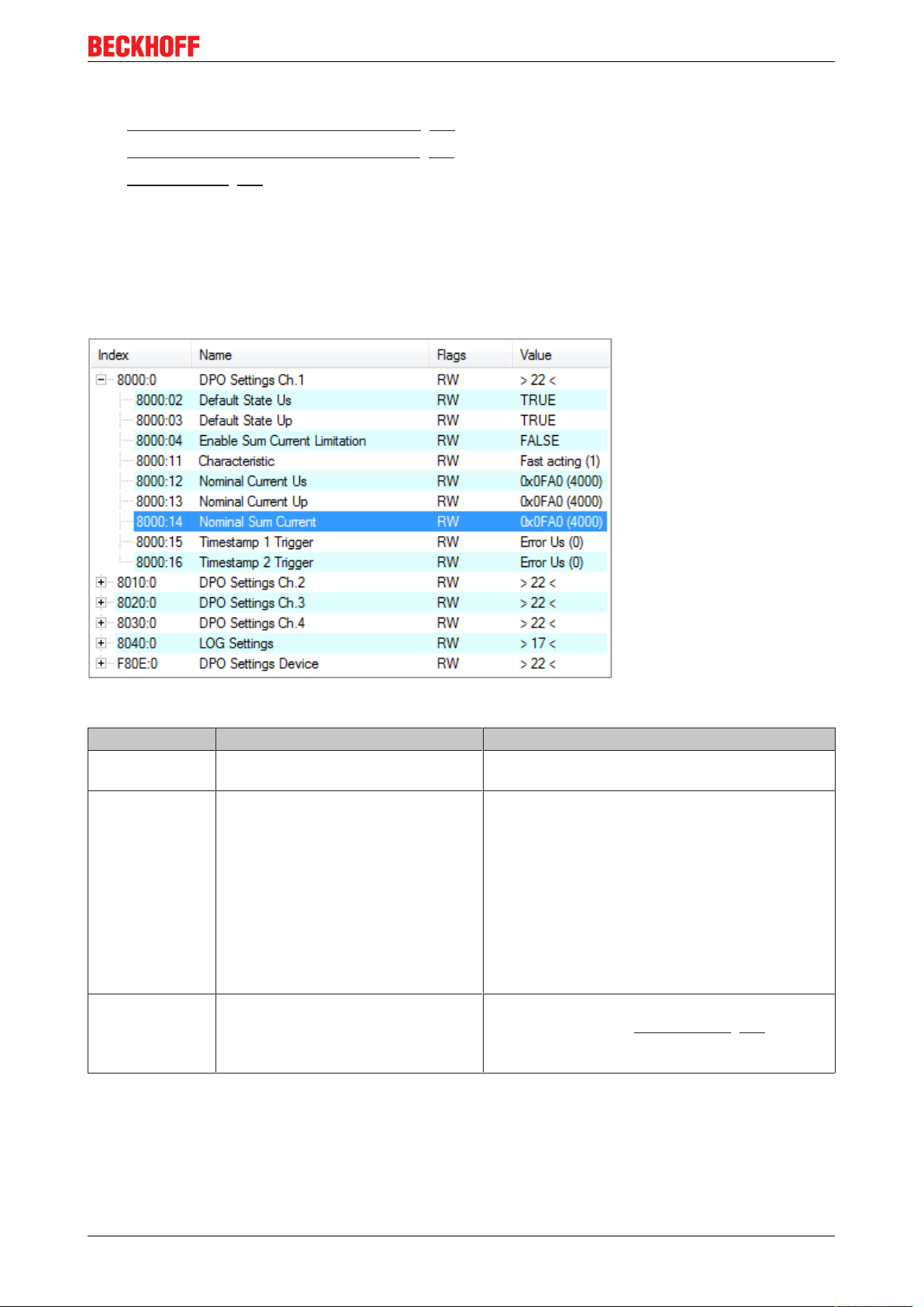
Comissioning and Configuration
Additional properties
• Switch-off due to sum current monitoring [}67]
• Extended diagnostic data by process data [}69]
• Data Logging [}73]
Additional settings in the CoE
Settings for each output channel
The object 80n0:04 must be activated in order to activate the sum current limitation.
The sum current can then be defined in the object 80n0:14.
Fig.51: Object 8000:14 Nominal Sum Current
CoE Title Description
80n0:04 Enable Sum Current Limitation The CoE object 80n0:04 must be set to TRUE in
order to activate 80n0:14
80n0:14 Nominal Sum Current Apart from the nominal current for each Us and Up
(basic function of the EP92x4), the sum current of
both outputs can also be limited per channel.
This property is recommended if the end device
may not exceed a total power.
The default value is 4.0A (4000), the maximum
sum current 8A.
The sum current switch-off corresponds to the
behavior of the load circuit concerned (CoE
80n0:11).
80n0:15 / 16 Timestamp n Trigger On occurrence of the selected event, the
corresponding value (Peak Value n [}69]) and
the appropriate timestamp are set in the process
data.
If overcurrent (≥ nominal current) is detected and it is foreseeable that the current monitoring will trip if
conditions remain unchanged, then a warning is given both in the process data and in form of a flashing
LED. An output switch-off due to overcurrent is indicated by a red LED.
If one of the outputs was switched off due to a diagnosis, it must be reactivated by an active RESET.
EP9214-0023 and EP9224-0023 67Version: 2.3.1
Page 68

Comissioning and Configuration
Restart after Power OFF/ON
If an output was switched off due to an error, then an active reset by the RESET contact or
Note
Switching on can be done either via EtherCAT or by applying 24V to the RESET contact. To protect the
circuitry, a RESET can take place maximally every 20seconds. Faster successive edges are ignored.
Additional diagnosis
Extended diagnosis [}69] and data logging [}73]
the fieldbus is necessary. Switching off and on again is not sufficient!
4.6.1.2 Additional PDOs of the EP9224
The selection of additional PDOs in the PDO Mapping is required for the use of the diagnostic functions.
This allows the display of further diagnostic data [}69] in the process data section.
Additional input PDOs
Fig.52: EP9224 - Additional input PDOs
EP9214-0023 and EP9224-002368 Version: 2.3.1
Page 69

Additional output PDOs
Comissioning and Configuration
Fig.53: EP9224 - Additional output PDOs
4.6.1.3 Extended channel and device diagnosis of the EP9224
The selection of additional PDOs in the PDO Mapping is required for the use of the diagnostic functions.
Certain values can be recorded with time stamp (timestamp / trigger [}71]) for each channel of DPO
Extended Diag Inputs Channel n and for the DPO Extended Diag Inputs Device module.
DPO Extended Diag Output Device resets the recording.
DPO Extended Diag Inputs Channel n
The DPO Extended Diag Inputs Channel n can be activated with each channel.
It continuously indicates the respective current value Peak Value n and the precise time of the arrival
Timestamp n.
The selection of the triggering event takes place in the CoE object 80x0:15 or 16.
EP9214-0023 and EP9224-0023 69Version: 2.3.1
Page 70

Comissioning and Configuration
Fig.54: EP9224 - DPO Extended Diag Inputs Channel 1
DPO Extended Diag Inputs Device
As for each channel there is also a DPO Extended Diag Inputs Device for the entire EP9224.
It continuously indicates the respective current value Peak Value n and the precise time of the arrival
Timestamp n.
The selection of the triggering event takes place in the CoE object F80E:15 or 16.
Fig.55: EP9224 - DPO Extended Diag Inputs Device
DPO Extended Diag Outputs Channel n
The Peak Value and Timestamp data of the respective channel are reset by setting the Reset Extended Diag
Data bit.
The bit is state-triggered.
Fig.56: EP9224 - DPO Extended Diag Outputs Channel 1
EP9214-0023 and EP9224-002370 Version: 2.3.1
Page 71
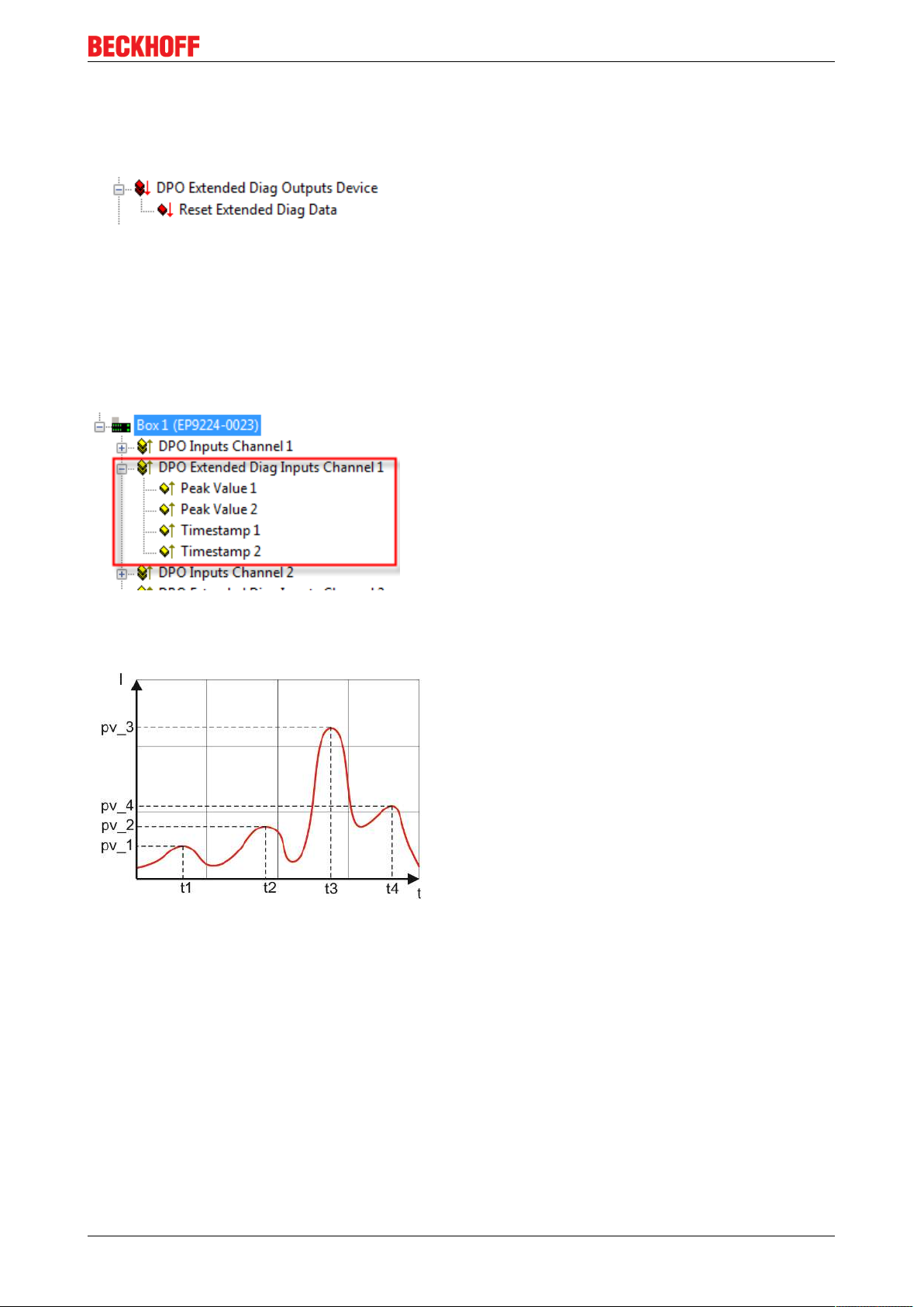
Comissioning and Configuration
DPO Extended Diag Outputs Device
The Peak Value and Timestamp data of the module are reset by setting the Reset Extended Diag Data bit.
The bit is state-triggered.
Fig.57: EP9224 - DPO Extended Diag Outputs Device
4.6.1.4 Timestamp / trigger of the EP9224
The last min/max values Peak Value n and the respective timestamp Timestamp n can be displayed or
recorded via the Timestamp/ Trigger setting, depending on the trigger criterion in the CoE 80n0:15 and 16.
Process data
Fig.58: EP9224 - process data
Peak value / Timstamp
Fig.59: EP9224 - Peak value / Timstamp
The present value and the associated timestamp are set each time the value momentarily saved in Peak
Value n is exceeded or fallen below.
Thus, for example, in the above case with the setting Maximum Current Us, the value pv_3 is displayed in
the process data with the timestamp t3.
Selection of the trigger criterion
Settings for each output channel
The object 80n0:15 or 16 must be adapted for the selection.
EP9214-0023 and EP9224-0023 71Version: 2.3.1
Page 72

Comissioning and Configuration
Fig.60: EP9224 - Selection of the trigger criterion - Settings for each output channel
Description of the setting
CoE Title Description
80n0:15 / 16 Error Us Switch-off of Us due to an error (edge triggered 0->1)
Error Up Switch-off of Up due to an error (edge triggered 0->1)
Warning Us Imminent switch-off of Us due to a continuous overload >
100% (edge triggered 0->1)
Warning Up Imminent switch-off of Up due to a continuous overload >
100% (edge triggered 0->1)
Error Sum Current Switch-off of Us and Up due to a total current error (edge
triggered 0->1)
Warning Sum Current Imminent switch-off of Us and Up due to a total current error
(edge triggered 0->1)
Minimum Current Us Minimum current on Us
Maximum Current Us Maximum current on Us
Minimum Current Up Minimum current on Up
Maximum Current Up Maximum current on Up
EP9214-0023 and EP9224-002372 Version: 2.3.1
Page 73

Reset of the values
Reset of Peak Value n and Timestamp for each channel
Fig.61: EP9224 - Reset extended diag data for the channel
Reset of Peak Value n and Timestamp of the module
Comissioning and Configuration
Fig.62: EP9224 - Reset extended diag data for the module
4.6.1.5 Data logging
Overview
With the data logging the continuous logging of all relevant EP9224 data can be started.
These data are written to a 40-line ring buffer.
On the first error the recording is stopped so that the data can be evaluated after an error or during normal
operation.
In the event of an error, data are still written for a few cycles. The switching-off of a channel is indicated by
OFF.
The writing rate or scanning rate is 10ms in the factory setting. The value can be adjusted from 1ms to
1000ms in the CoE.
EP9214-0023 and EP9224-0023 73Version: 2.3.1
Page 74

Comissioning and Configuration
Setting of the scanning rate via CoE object 8040:11
Fig.63: EP9224 - Setting of the scanning rate
Starting the logger
The logger is started/stopped via the process data
• Start logger and
• Stop logger
These must be activated via the PDO mapping 0x1610 (see PDO settings [}68]).
DPO LOG Control
Fig.64: EP9224 - DPO LOG Control
The log file is written when stopping the logger or in the case of an error.
The state of the logger can be tracked in the PDO input area.
To do this it is necessary to activate the PDO 0x1A10 (see PDO settings [}68]).
EP9214-0023 and EP9224-002374 Version: 2.3.1
Page 75

DPO LOG Status
Fig.65: EP9224 - DPO LOG Status
Comissioning and Configuration
Upload the file from the EP9224
The EP9224 creates the file, giving it the name logdata.csv. This cannot be changed.
When uploading, for example, it must be specified accordingly in TwinCAT.
EP9214-0023 and EP9224-0023 75Version: 2.3.1
Page 76
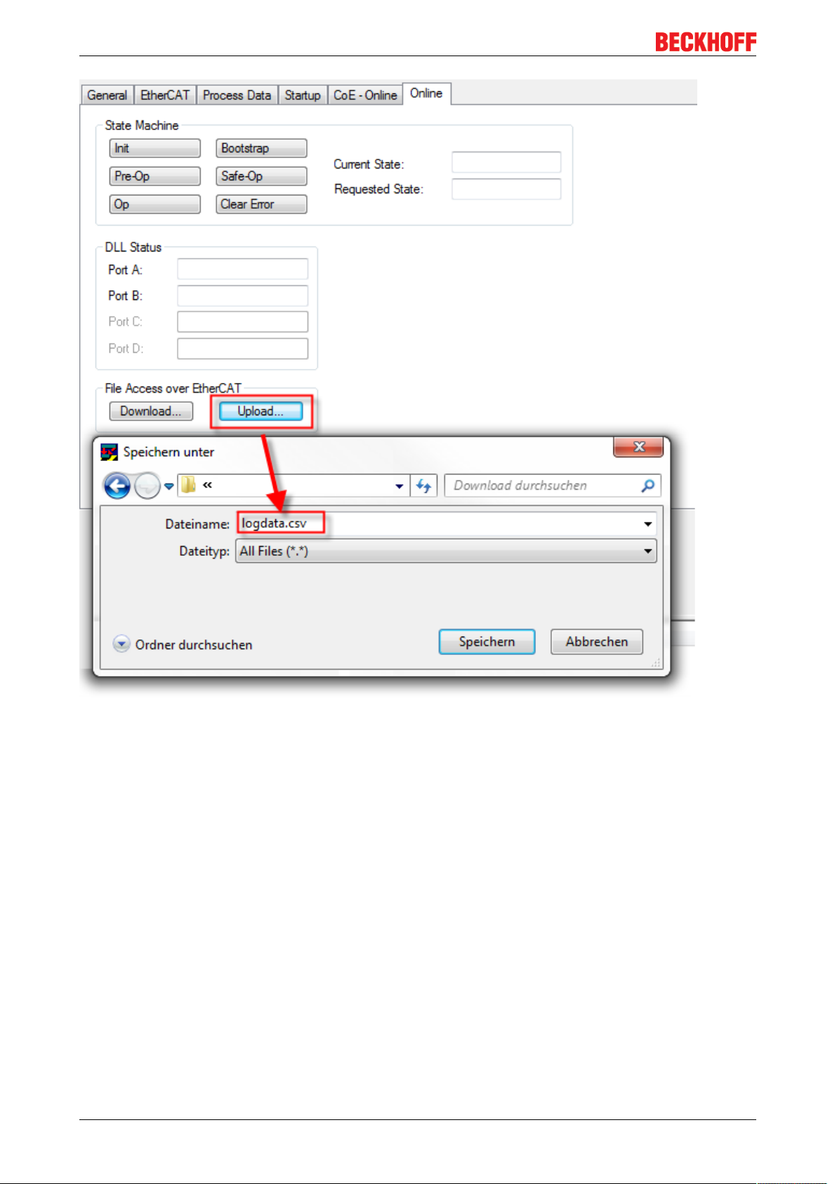
Comissioning and Configuration
Fig.66: EP9224 - Uploading the file
Structure of the logging file: logdata.csv
The data are saved in the CSV format, so that simple viewing with EXCEL or a corresponding interpretation
is possible.
EP9214-0023 and EP9224-002376 Version: 2.3.1
Page 77

Comissioning and Configuration
Fig.67: EP9224 - Structure of the file: logdata.csv
Header
Type Description
Device name Name of the module
File Version Version number (note: when importing from EXCEL the version, e.g.
1.5, is interpreted/displayed as a date (1st May))
Reason for which the snapshot
was taken
Age of snapshot Period elapsed between preparing the file and the upload
System timestamp (0 if DC not
supported)
Cause of switching off the data logger
current time stamp when uploading
Columns
Type Description
Time offset additional to snapshot
age
I(U...) present current values of the channels Us / Up 1 - 4 in 100mA
Internal Temperature internal module temperature in °C
Us / Up Input voltage Us and Up at the 7/8" input in V
Sum Current Us / Up Sum current of Us and Up in A
I²t(U...) virtual overload, incremented or decremented depending on the nominal
Example: slow exceeding of the current (simulation with potentiometer)
logdata.csv (zip)
The age of the measured values in the row in relation to the stopping of
the data logger (0 = stop, > 0 older values) in ms
current
• from 10% warning
• at 100% shut-off
EP9214-0023 and EP9224-0023 77Version: 2.3.1
Page 78

Comissioning and Configuration
Fig.68: EP9224 - logdata.csv
Description:
• EP9224: Setting the Us channel to a nominal current of 1500mA
• Continuous increase of the current on channel 1 Us within the recorded range of 3.0A to 4.9A, then
shut-off takes place.
• Overcurrent begins from 180ms
• 100% overload reached (99), channel is switched off
• the module now waits for an error correction or an active reset of the error
EP9214-0023 and EP9224-002378 Version: 2.3.1
Page 79

Comissioning and Configuration
4.6.2 EP9224-0023 - Object description
Parameterization
Terminals' parameterization will be conducted by the CoE tab (double-click on the referring
Note
Note
The CoE overview contains objects for different intended applications:
• Objects required for parameterization during commissioning
• Objects intended for regular operation e.g. through ADS access
• Objects for indicating internal settings (may be fixed)
• Further profile-specific objects indicating inputs, outputs and status information
The following section first describes the objects require for normal operation, followed by a complete
overview of missing objects.
object) or the Process data tab (PDO assignment)
EtherCAT XML Device Description
The description correspond to the display of the CoE objects from the EtherCAT XML Device Description. It is strongly recommended to download the latest revision of the corresponding XML file from the Beckhoff website (http://www.beckhoff.com/english/default.htm?
download/elconfg.htm) and follow the installation instructions.
4.6.2.1 Objects for parameterization
4.6.2.1.1 Index 1011 Restore default parameters
Index Name Meaning Data type Flags Default
1011:0 Restore default
parameters
1011:01 SubIndex 001 If this object is set to 0x64616F6C in the set value di-
Restore default parameters UINT8 RO 0x01 (1
UINT32 RW 0x00000000 (0
alog, all backup objects are reset to their delivery
state.
)
dec
)
dec
EP9214-0023 and EP9224-0023 79Version: 2.3.1
Page 80

Comissioning and Configuration
4.6.2.1.2 Index 8000 DPO Settings Ch.1
Index Name Meaning Data type Flags Default
8000:0 DPO Set-
tings Ch.1
8000:02 Default
State Us
8000:03 Default
State Up
8000:04 Enable Sum
Current Limitation
8000:11 Characteris-
tic
8000:12 Nominal
Current Us
8000:13 Nominal
Current Up
8000:14 Nominal
Sum Current
8000:15 Timestamp
1 Trigger
8000:16 Timestamp
2 Trigger
The output adopts this value if Enable Control via
Fieldbus (F707:01) is not set or no connection to the
fieldbus
The output adopts this value if Enable Control via
Fieldbus (F707:01) is not set or no connection to the
fieldbus
Sum current limitation:
0
: disabled
bin
1
: enabled
bin
Specifies the characteristic with which the current
monitoring reacts:
0
: very fast acting
dec
1
: fast acting
dec
2
: slow acting
dec
3
: time delay
dec
Nominal current at the output UINT16 RW 0x0FA0 (4000
Nominal current at the output UINT16 RW 0x0FA0 (4000
Nominal total current UINT16 RW 0x0FA0 (4000
Trigger condition for extended diagnosis UINT16 RW 0x0000 (0
Trigger condition for extended diagnosis UINT16 RW 0x0000 (0
UINT8 RO 0x16 (22
boolean RW 0x01 (1
boolean RW 0x01 (1
boolean RW 0x00 (0
UINT16 RW 0x0001 (1
)
dec
)
dec
)
dec
)
dec
)
dec
)
dec
)
dec
)
dec
)
dec
)
dec
4.6.2.1.3 Index 8010 DPO Settings Ch.2
Index Name Meaning Data type Flags Default
8010:0 DPO Set-
tings Ch.2
8010:02 Default
State Us
8010:03 Default
State Up
8010:04 Enable Sum
Current Limitation
8010:11 Characteris-
tic
8010:12 Nominal
Current Us
8010:13 Nominal
Current Up
8010:14 Nominal
Sum Current
8010:15 Timestamp
1 Trigger
8010:16 Timestamp
2 Trigger
The output adopts this value if Enable Control via
Fieldbus (F707:01) is not set or no connection to the
fieldbus
The output adopts this value if Enable Control via
Fieldbus (F707:01) is not set or no connection to the
fieldbus
Sum current limitation:
0
: disabled
bin
1
: enabled
bin
Specifies the characteristic with which the current
monitoring reacts:
0
: very fast acting
dec
1
: fast acting
dec
2
: slow acting
dec
3
: time delay
dec
Nominal current at the output UINT16 RW 0x0FA0 (4000
Nominal current at the output UINT16 RW 0x0FA0 (4000
Nominal total current UINT16 RW 0x0FA0 (4000
Trigger condition for extended diagnosis UINT16 RW 0x0000 (0
Trigger condition for extended diagnosis UINT16 RW 0x0000 (0
UINT8 RO 0x16 (22
boolean RW 0x01 (1
boolean RW 0x01 (1
boolean RW 0x00 (0
UINT16 RW 0x0001 (1
)
dec
)
dec
)
dec
)
dec
)
dec
)
dec
)
dec
)
dec
)
dec
)
dec
EP9214-0023 and EP9224-002380 Version: 2.3.1
Page 81

Comissioning and Configuration
4.6.2.1.4 Index 8020 DPO Settings Ch.3
Index Name Meaning Data type Flags Default
8020:0 DPO Set-
tings Ch.3
8020:02 Default
State Us
8020:03 Default
State Up
8020:04 Enable Sum
Current Limitation
8020:11 Characteris-
tic
8020:12 Nominal
Current Us
8020:13 Nominal
Current Up
8020:14 Nominal
Sum Current
8020:15 Timestamp
1 Trigger
8020:16 Timestamp
2 Trigger
The output adopts this value if Enable Control via
Fieldbus (F707:01) is not set or no connection to the
fieldbus
The output adopts this value if Enable Control via
Fieldbus (F707:01) is not set or no connection to the
fieldbus
Sum current limitation:
0
: disabled
bin
1
: enabled
bin
Specifies the characteristic with which the current
monitoring reacts:
0
: very fast acting
dec
1
: fast acting
dec
2
: slow acting
dec
3
: time delay
dec
Nominal current at the output UINT16 RW 0x0FA0 (4000
Nominal current at the output UINT16 RW 0x0FA0 (4000
Nominal total current UINT16 RW 0x0FA0 (4000
Trigger condition for extended diagnosis UINT16 RW 0x0000 (0
Trigger condition for extended diagnosis UINT16 RW 0x0000 (0
UINT8 RO 0x16 (22
boolean RW 0x01 (1
boolean RW 0x01 (1
boolean RW 0x00 (0
UINT16 RW 0x0001 (1
)
dec
)
dec
)
dec
)
dec
)
dec
)
dec
)
dec
)
dec
)
dec
)
dec
4.6.2.1.5 Index 8030 DPO Settings Ch.4
Index Name Meaning Data type Flags Default
8030:0 DPO Set-
tings Ch.4
8030:02 Default
State Us
8030:03 Default
State Up
8030:04 Enable Sum
Current Limitation
8030:11 Characteris-
tic
8030:12 Nominal
Current Us
8030:13 Nominal
Current Up
8030:14 Nominal
Sum Current
8030:15 Timestamp
1 Trigger
8030:16 Timestamp
2 Trigger
The output adopts this value if Enable Control via
Fieldbus (F707:01) is not set or no connection to the
fieldbus
The output adopts this value if Enable Control via
Fieldbus (F707:01) is not set or no connection to the
fieldbus
Sum current limitation:
0
: disabled
bin
1
: enabled
bin
Specifies the characteristic with which the current
monitoring reacts:
0
: very fast acting
dec
1
: fast acting
dec
2
: slow acting
dec
3
: time delay
dec
Nominal current at the output UINT16 RW 0x0FA0 (4000
Nominal current at the output UINT16 RW 0x0FA0 (4000
Nominal total current UINT16 RW 0x0FA0 (4000
Trigger condition for extended diagnosis UINT16 RW 0x0000 (0
Trigger condition for extended diagnosis UINT16 RW 0x0000 (0
UINT8 RO 0x16 (22
boolean RW 0x01 (1
boolean RW 0x01 (1
boolean RW 0x00 (0
UINT16 RW 0x0001 (1
)
dec
)
dec
)
dec
)
dec
)
dec
)
dec
)
dec
)
dec
)
dec
)
dec
EP9214-0023 and EP9224-0023 81Version: 2.3.1
Page 82

Comissioning and Configuration
4.6.2.1.6 Index 8040 LOG Settings
Index Name Meaning Data type Flags Default
8040:0 LOG Set-
tings
8040:11 Sampling
Rate
permitted values:
1: 1ms
10: 10ms
25: 25ms
100: 100ms
UINT8 RO 0x11 (17
UINT16 RW 0x000A (10
)
dec
)
dec
EP9214-0023 and EP9224-002382 Version: 2.3.1
Page 83

Comissioning and Configuration
4.6.2.1.7 Index F607 DPO Inputs Device
Index Name Meaning Data type Flags Default
F607:0 DPO Inputs Device UINT8 RO 0x19 (25
F607:01 Temperature Warning A temperature of about 80°C
has been reached
F607:02 Temperature Error A critical temperature of about
85°C has been reached, the
outputs will be switched off. The
bit must be reset by a Global
Reset (F707:04) or by a voltage
reset. No output can be
switched on if the error bit is
set.
F607:03 Us Warning Us is less than 21.5V, no fur-
ther outputs can be switched
on.
F607:04 Us Error Us is less than 19V, all Us out-
puts will be switched off. The bit
must be reset by a Global Re-
set (F707:04) or by a voltage
reset. No Us output can be
switched on if the error bit is
set.
F607:05 Up Warning Up is less than 21.5V, no fur-
ther outputs can be switched
on.
F607:06 Up Error Up is less than 19V, all Up out-
puts will be switched off. The bit
must be reset by a Global Re-
set (F707:04) or by a voltage
reset. No Up output can be
switched on if the error bit is
set.
F607:07 Global Error Bit One of the error bits of the four
channels or F607:02 or F607:04
or F607:06 is set
F607:08 Sum Current Warning Sum current monitoring has de-
sected a peak current
F607:09 Sum Current Error Sum current monitoring has de-
sected an over current. All outputs are switched off
F607:0C Reset Input Us is less than 21.5V, no fur-
ther outputs can be switched
on.
F607:0F TxPDO State boolean RO 0x00 (0
F607:10 TxPDO Toggle boolean RO 0x00 (0
F607:11 Current Us Sum current of the module atUsINT16 RO 0x0000 (0
boolean RO 0x00 (0
boolean RO 0x00 (0
boolean RO 0x00 (0
boolean RO 0x00 (0
boolean RO 0x00 (0
boolean RO 0x00 (0
boolean RO 0x00 (0
boolean RO 0x00 (0
boolean RO 0x00 (0
boolean RO 0x00 (0
dec
dec
dec
dec
dec
dec
dec
dec
dec
dec
dec
dec
)
dec
)
)
)
)
)
)
)
)
)
)
)
)
)
dec
F607:12 Current Up Sum current of the module atUpINT16 RO 0x0000 (0
F607:13 Voltage Us Voltage at input Us INT16 RO 0x0000 (0
F607:14 Voltage Up Voltage at input Up INT16 RO 0x0000 (0
F607:15 Temperature Internal temperature of power
INT16 RO 0x0000 (0
stage
F607:16 Peak Value 1 Extended diagnosis INT16 RO 0x0000 (0
F607:17 Peak Value 2 Extended diagnosis INT16 RO 0x0000 (0
F607:18 Timestamp 1 UINT64 RO
F607:19 Timestamp 2 UINT64 RO
EP9214-0023 and EP9224-0023 83Version: 2.3.1
)
dec
)
dec
)
dec
)
dec
)
dec
)
dec
Page 84

Comissioning and Configuration
4.6.2.1.8 Index F707 DPO Outputs Device
Index Name Meaning Data type Flags Default
F707:0 DPO Out-
puts Device
F707:01 Enable Con-
trol Via
Fieldbus
F707:04 Global Re-
set
F707:11 Reset Ex-
tended Diag
Data
0
: All outputs are set to their default values
bin
(80X0:02, 80X0:03)
1
: All outputs are set according to their PDOs
bin
(70X0:01, 70X0:02)
All error bits are reset boolean RO 0x00 (0
Peak Values and time stamps from F607 are reset boolean RO 0x00 (0
UINT8 RO 0x11 (17
boolean RO 0x00 (0
)
dec
)
dec
)
dec
)
dec
EP9214-0023 and EP9224-002384 Version: 2.3.1
Page 85

Comissioning and Configuration
4.6.2.1.9 Index F80E DPO Settings Device
Index Name Meaning Data type Flags Default
F80E:0 DPO Set-
tings Device
F80E:02 Enable Sum
Current Limitation
F80E:03 Automatic
Restart After Uncritic
Events on
Us
F80E:04 Automatic
Restart After Uncritic
Events on
Up
F80E:11 Startup De-
lay
F80E:12 Nominal
Sum Current
F80E:13 Sum Cur-
rent Characteristic
F80E:15 Timestamp
1 Trigger
F80E:16 Timestamp
2 Trigger
Sum Current monitoring:
0
: enabled
bin
1
: disabled
bin
Switch on automatically after undervoltage und
overtemperature:
0
: enabled
bin
1
: disabled
bin
Switch on automatically after undervoltage und
overtemperature:
0
: enabled
bin
1
: disabled
bin
Sets the time that is kept between two switch-on procedures:
1
: fast (10ms)
dec
2
: moderate (100ms)
dec
3
: slow (200ms)
dec
Nominal sum current INT16 RW 0x2710 (10000
Characteristic of sum current monitoring UINT16 RW 0x0001 (1
Item that ist to be monitored for extended diagnosis:
0: Temperature Warning
1: Temperature Error
2: Us Warning
3: Us Error
4: Up Warning
5: Up Error
6: Global Error Bit
7: Sum Current Warning
8: Sum Current Error
16: Minmum Current Us
17: Maximum Current Us
18: Minimum Current Up
19: Maximum Current Up
20: Minimum Voltage Us
21: Maximum Voltage Us
22: Minimum Voltage Up
23: Maximum Voltage Up
25: Maximum Temperature
24: Minimum Temperature
UINT8 RO 0x16 (22
boolean RW 0x00 (0
boolean RW 0x00 (0
boolean RW 0x00 (0
UINT16 RW 0x0001 (1
UINT16 RW 0x0000 (0
UINT16 RW 0x0000 (0
)
dec
)
dec
)
dec
)
dec
)
dec
)
dec
)
dec
)
dec
)
dec
EP9214-0023 and EP9224-0023 85Version: 2.3.1
Page 86

Comissioning and Configuration
4.6.2.2 Standard objects
The standard objects have the same meaning for all EtherCAT slaves.
4.6.2.2.1 Index 1000 Device type
Index Name Meaning Data type Flags Default
1000:0 Device type Device type of the EtherCAT slave: the Lo-Word con-
tains the CoE profile used (5001). The Hi-Word contains the module profile according to the modular device profile.
4.6.2.2.2 Index 1008 Device name
Index Name Meaning Data type Flags Default
1008:0 Device name Device name of the EtherCAT slave STRING RO EP9224-0023
4.6.2.2.3 Index 1009 Hardware version
Index Name Meaning Data type Flags Default
1009:0 Hardware ver-
sion
Hardware version of the EtherCAT slave STRING RO
UINT32 RO 0x00001389 (5001
)
dec
4.6.2.2.4 Index 100A Software version
Index Name Meaning Data type Flags Default
100A:0 Software ver-
Firmware version of the EtherCAT slave STRING RO 01
sion
4.6.2.2.5 Index 1018 Identity
Index Name Meaning Data type Flags Default
1018:0 Identity Information for identifying the slave UINT8 RO 0x04 (4
)
dec
1018:01 Vendor ID Vendor ID of the EtherCAT slave UINT32 RO 0x00000002 (2
1018:02 Product code Product code of the EtherCAT slave UINT32 RO 0x24084052
1018:03 Revision Revision numberof the EtherCAT slave; the low word
(604520530
UINT32 RO 0x00000000 (0
dec
(bit 0-15) indicates the special terminal number, the
high word (bit 16-31) refers to the device description
1018:04 Serial number Serial number of the EtherCAT slave; the low byte
UINT32 RO 0x00000000 (0
(bit 0-7) of the low word contains the year of production, the high byte (bit 8-15) of the low word contains
the week of production, the high word (bit 16-31) is 0
4.6.2.2.6 Index 10F0 Backup parameter handling
Index Name Meaning Data type Flags Default
10F0:0 Backup pa-
rameter handling
10F0:01 Checksum Checksum across all backup entries of the EtherCAT
Information for standardized loading and saving of
backup entries
slave
UINT8 RO 0x01 (1
)
dec
UINT32 RO 0x00000000 (0
)
dec
)
)
dec
)
dec
)
dec
EP9214-0023 and EP9224-002386 Version: 2.3.1
Page 87

Comissioning and Configuration
4.6.2.2.7 Index 1600 DPO RxPDO-Map Outputs Ch.1
Index Name Meaning Data type Flags Default
1600:0 DPO RxPDO-
Map Outputs
PDO Mapping RxPDO 1 UINT8 RO 0x06 (6
)
dec
Ch.1
1600:01 SubIndex 001 1. PDO Mapping entry (object 0x7000 (DPO Outputs
UINT32 RO 0x7000:01, 1
Ch.1), entry 0x01 (Output Us))
1600:02 SubIndex 002 2. PDO Mapping entry (object 0x7000 (DPO Outputs
UINT32 RO 0x7000:02, 1
Ch.1), entry 0x02 (Output Up))
1600:03 SubIndex 003 3. PDO Mapping entry (2 bits align) UINT32 RO 0x0000:00, 2
1600:04 SubIndex 004 4. PDO Mapping entry (object 0x7000 (DPO Outputs
UINT32 RO 0x7000:05, 1
Ch.1), entry 0x05 (Reset Us))
1600:05 SubIndex 005 5. PDO Mapping entry (object 0x7000 (DPO Outputs
UINT32 RO 0x7000:06, 1
Ch.1), entry 0x06 (Reset Up))
1600:06 SubIndex 006 6. PDO Mapping entry (10 bits align) UINT32 RO 0x0000:00, 10
4.6.2.2.8 Index 1601 DPO RxPDO-Map Extended Diag Outputs Ch.1
Index Name Meaning Data type Flags Default
1601:0 DPO RxPDO-
Map Extended
Diag Outputs
Ch.1
1601:01 SubIndex 001 1. PDO Mapping entry (object 0x7010 (DPO Outputs
1601:02 SubIndex 002 2. PDO Mapping entry (object 0x7010 (DPO Outputs
PDO Mapping RxPDO 2 UINT8 RO 0x02 (2
UINT32 RO 0x7000:11, 1
Ch.2), entry 0x01 (Output Us))
UINT32 RO 0x0000:00, 15
Ch.2), entry 0x02 (Output Up))
)
dec
4.6.2.2.9 Index 1602 DPO RxPDO-Map Outputs Ch.2
Index Name Meaning Data type Flags Default
1602:0 DPO RxPDO-
Map Outputs
PDO Mapping RxPDO 3 UINT8 RO 0x06 (6
)
dec
Ch.2
1602:01 SubIndex 001 1. PDO Mapping entry (object 0x7020 (DPO Outputs
UINT32 RO 0x7010:01, 1
Ch.3), entry 0x01 (Output Us))
1602:02 SubIndex 002 2. PDO Mapping entry (object 0x7020 (DPO Outputs
UINT32 RO 0x7010:02, 1
Ch.3), entry 0x02 (Output Up))
1602:03 SubIndex 003 3. PDO Mapping entry (2 bits align) UINT32 RO 0x0000:00, 2
1602:04 SubIndex 004 4. PDO Mapping entry (object 0x7020 (DPO Outputs
UINT32 RO 0x7010:05, 1
Ch.3), entry 0x05 (Reset Us))
1602:05 SubIndex 005 5. PDO Mapping entry (object 0x7020 (DPO Outputs
UINT32 RO 0x7010:06, 1
Ch.3), entry 0x06 (Reset Up))
1602:06 SubIndex 006 6. PDO Mapping entry (10 bits align) UINT32 RO 0x0000:00, 10
4.6.2.2.10 Index 1603 DPO RxPDO-Map Extended Diag Outputs Ch.2
Index Name Meaning Data type Flags Default
1603:0 DPO RxPDO-
Map Extended
Diag Outputs
Ch.2
1603:01 SubIndex 001 1. PDO Mapping entry (object 0x7030 (DPO Outputs
1603:02 SubIndex 002 2. PDO Mapping entry (object 0x7030 (DPO Outputs
PDO Mapping RxPDO 4 UINT8 RO 0x02 (2
UINT32 RO 0x7010:11, 1
Ch.4), entry 0x01 (Output Us))
UINT32 RO 0x0000:00, 15
Ch.4), entry 0x02 (Output Up))
)
dec
EP9214-0023 and EP9224-0023 87Version: 2.3.1
Page 88

Comissioning and Configuration
4.6.2.2.11 Index 1604 DPO RxPDO-Map Outputs Ch.3
Index Name Meaning Data type Flags Default
1604:0 DPO RxPDO-
Map Outputs
PDO Mapping RxPDO 5 UINT8 RO 0x06 (6
)
dec
Ch.3
1604:01 SubIndex 001 1. PDO Mapping entry (object 0x7020 (DPO Outputs
UINT32 RO 0x7020:01, 1
Ch.3), entry 0x01 (Output Us))
1604:02 SubIndex 002 2. PDO Mapping entry (object 0x7020 (DPO Outputs
UINT32 RO 0x7020:02, 1
Ch.3), entry 0x02 (Output Up))
1604:03 SubIndex 003 3. PDO Mapping entry (2 bits align) UINT32 RO 0x0000:00, 2
1604:04 SubIndex 004 4. PDO Mapping entry (object 0x7020 (DPO Outputs
UINT32 RO 0x7020:05, 1
Ch.3), entry 0x05 (Reset Us))
1604:05 SubIndex 005 5. PDO Mapping entry (object 0x7020 (DPO Outputs
UINT32 RO 0x7020:06, 1
Ch.3), entry 0x06 (Reset Up))
1604:06 SubIndex 006 6. PDO Mapping entry (10 bits align) UINT32 RO 0x0000:00, 10
4.6.2.2.12 Index 1605 DPO RxPDO-Map Extended Diag Outputs Ch.3
Index Name Meaning Data type Flags Default
1605:0 DPO RxPDO-
Map Extended
Diag Outputs
Ch.3
1605:01 SubIndex 001 1. PDO Mapping entry (object 0x7020 (DPO Outputs
1605:02 SubIndex 002 2. PDO Mapping entry (15 bits align) UINT32 RO 0x0000:00, 15
PDO Mapping RxPDO 6 UINT8 RO 0x02 (2
UINT32 RO 0x7020:11, 1
Ch.3), entry 0x11 (Reset Extended Diag Data))
)
dec
4.6.2.2.13 Index 1606 DPO RxPDO-Map Outputs Ch.4
Index Name Meaning Data type Flags Default
1606:0 DPO RxPDO-
Map Outputs
PDO Mapping RxPDO 7 UINT8 RO 0x06 (6
)
dec
Ch.4
1606:01 SubIndex 001 1. PDO Mapping entry (object 0x7030 (DPO Outputs
UINT32 RO 0x7030:01, 1
Ch.4), entry 0x01 (Output Us))
1606:02 SubIndex 002 2. PDO Mapping entry (object 0x7030 (DPO Outputs
UINT32 RO 0x7030:02, 1
Ch.4), entry 0x02 (Output Up))
1606:03 SubIndex 003 3. PDO Mapping entry (2 bits align) UINT32 RO 0x0000:00, 2
1606:04 SubIndex 004 4. PDO Mapping entry (object 0x7030 (DPO Outputs
UINT32 RO 0x7030:05, 1
Ch.4), entry 0x05 (Reset Us))
1606:05 SubIndex 005 5. PDO Mapping entry (object 0x7030 (DPO Outputs
UINT32 RO 0x7030:06, 1
Ch.4), entry 0x06 (Reset Up))
1606:06 SubIndex 006 6. PDO Mapping entry (10 bits align) UINT32 RO 0x0000:00, 10
4.6.2.2.14 Index 1607 DPO RxPDO-Map Extended Diag Outputs Ch.4
Index Name Meaning Data type Flags Default
1607:0 DPO RxPDO-
Map Extended
Diag Outputs
Ch.4
1607:01 SubIndex 001 1. PDO Mapping entry (object 0x7030 (DPO Outputs
1607:02 SubIndex 002 2. PDO Mapping entry (15 bits align) UINT32 RO 0x0000:00, 15
PDO Mapping RxPDO 8 UINT8 RO 0x02 (2
UINT32 RO 0x7030:11, 1
Ch.4), entry 0x11 (Reset Extended Diag Data))
)
dec
EP9214-0023 and EP9224-002388 Version: 2.3.1
Page 89

Comissioning and Configuration
4.6.2.2.15 Index 1608 DPO RxPDO-Map Outputs Device
Index Name Meaning Data type Flags Default
1608:0 DPO RxPDO-
Map Outputs
PDO Mapping RxPDO 9 UINT8 RO 0x04 (4
)
dec
Device
1608:01 SubIndex 001 1. PDO Mapping entry (object 0xF707 (DPO Outputs
UINT32 RO 0xF707:01, 1
Device), entry 0x01 (Enable Control Via Fieldbus))
1608:02 SubIndex 002 2. PDO Mapping entry (2 bits align) UINT32 RO 0x0000:00, 2
1608:03 SubIndex 003 3. PDO Mapping entry (object 0xF707 (DPO Outputs
UINT32 RO 0xF707:04, 1
Device), entry 0x04 (Global Reset))
1608:04 SubIndex 004 4. PDO Mapping entry (12 bits align) UINT32 RO 0x0000:00, 12
4.6.2.2.16 Index 1609 DPO RxPDO-Map Extended Diag Outputs Device
Index Name Meaning Data type Flags Default
1609:0 DPO RxPDO-
Map Extended
Diag Outputs
Device
1609:01 SubIndex 001 1. PDO Mapping entry (object 0xF707 (DPO Outputs
1609:02 SubIndex 002 2. PDO Mapping entry (15 bits align) UINT32 RO 0x0000:00, 15
PDO Mapping RxPDO 10 UINT8 RO 0x02 (2
UINT32 RO 0xF707:11, 1
Device), entry 0x11 (Reset Extended Diag Data))
)
dec
4.6.2.2.17 Index 1610 LOG RxPDO-Map Control
Index Name Meaning Data type Flags Default
1610:0 LOG Rx-
PDO-Map
Control
1610:01 SubIndex
001
1610:02 SubIndex
002
1610:03 SubIndex
003
PDO Mapping RxPDO 17 UINT8 RO 0x03 (3
1. PDO Mapping entry (object 0x7040 (LOG Control),
UINT32 RO 0x7040:01, 1
entry 0x01 (Start Logger))
2. PDO Mapping entry (object 0x7040 (LOG Control),
UINT32 RO 0x7040:02, 1
entry 0x02 (Stop Logger))
3. PDO Mapping entry (14 bits align) UINT32 RO 0x0000:00, 14
)
dec
EP9214-0023 and EP9224-0023 89Version: 2.3.1
Page 90

Comissioning and Configuration
4.6.2.2.18 Index 1A00 DPO TxPDO-Map Inputs Ch.1
Index Name Meaning Data type Flags Default
1A00:0 DPO Tx-
PDO-Map
Inputs Ch.1
1A00:01 SubIndex
001
1A00:02 SubIndex
002
1A00:03 SubIndex
003
1A00:04 SubIndex
004
1A00:05 SubIndex
005
1A00:06 SubIndex
006
1A00:07 SubIndex
007
1A00:08 SubIndex
008
1A00:09 SubIndex
009
1A00:0A SubIndex
010
1A00:0B SubIndex
011
1A00:0C SubIndex
012
1A00:0D SubIndex
013
1A00:0E SubIndex
014
PDO Mapping TxPDO 1 UINT8 RO 0x0E (14
1. PDO Mapping entry (object 0x6000 (DPO Inputs
Ch.1), entry 0x01 (Error Us))
2. PDO Mapping entry (object 0x6000 (DPO Inputs
Ch.1), entry 0x02 (Error Up))
3. PDO Mapping entry (object 0x6000 (DPO Inputs
Ch.1), entry 0x03 (Warning Us))
4. PDO Mapping entry (object 0x6000 (DPO Inputs
Ch.1), entry 0x04 (Warning Up))
5. PDO Mapping entry (object 0x6000 (DPO Inputs
Ch.1), entry 0x05 (Status Us))
6. PDO Mapping entry (object 0x6000 (DPO Inputs
Ch.1), entry 0x06 (Status Up))
7. PDO Mapping entry (object 0x6000 (DPO Inputs
Ch.1), entry 0x07 (Channel Error))
8. PDO Mapping entry (object 0x6000 (DPO Inputs
Ch.1), entry 0x08 (Error Sum Current))
9. PDO Mapping entry (object 0x6000 (DPO Inputs
Ch.1), entry 0x09 (Warning Sum Current))
10. PDO Mapping entry (4 bits align) UINT32 RO 0x0000:00, 5
11. PDO Mapping entry (object 0x6000 (DPO Inputs
Ch.1), entry 0x0E (Sync error))
12. PDO Mapping entry (object 0x6000 (DPO Inputs
Ch.1), entry 0x0F (TxPDO State))
13. PDO Mapping entry (object 0x6000 (DPO Inputs
Ch.1), entry 0x10 (TxPDO Toggle))
14. PDO Mapping entry (object 0x6000 (DPO Inputs
Ch.1), entry 0x11 (Current Us))
UINT32 RO 0x6000:01, 1
UINT32 RO 0x6000:02, 1
UINT32 RO 0x6000:03, 1
UINT32 RO 0x6000:04, 1
UINT32 RO 0x6000:05, 1
UINT32 RO 0x6000:06, 1
UINT32 RO 0x6000:07, 1
UINT32 RO 0x6000:08, 1
UINT32 RO 0x6000:09, 1
UINT32 RO 0x6000:0F, 1
UINT32 RO 0x6000:10, 1
UINT32 RO 0x6000:11, 16
UINT32 RO 0x6000:12, 16
)
dec
4.6.2.2.19 Index 1A01 DPO TxPDO-Map Extended Diag Inputs Ch.1
Index Name Meaning Data type Flags Default
1A01:0 DPO Tx-
PDO-Map
Extended
Diag Inputs
Ch.1
1A01:01 SubIndex
001
1A01:02 SubIndex
002
1A01:03 SubIndex
003
1A01:04 SubIndex
004
PDO Mapping TxPDO 2 UINT8 RO 0x04 (4
1. PDO Mapping entry (object 0x6000 (DPO Inputs
Ch.1), entry 0x13 (Maximum Current Us))
2. PDO Mapping entry (object 0x6000 (DPO Inputs
Ch.1), entry 0x14 (Maximum Current Up))
3. PDO Mapping entry (object 0x6000 (DPO Inputs
Ch.1), entry 0x15 (Minimum Current Us))
4. PDO Mapping entry (object 0x6000 (DPO Inputs
Ch.1), entry 0x16 (Minimum Current Up))
UINT32 RO 0x6000:13, 16
UINT32 RO 0x6000:14, 16
UINT32 RO 0x6000:17, 64
UINT32 RO 0x6000:18, 64
)
dec
EP9214-0023 and EP9224-002390 Version: 2.3.1
Page 91

Comissioning and Configuration
4.6.2.2.20 Index 1A02 DPO TxPDO-Map Inputs Ch.2
Index Name Meaning Data type Flags Default
1A02:0 DPO Tx-
PDO-Map
Inputs Ch.2
1A02:01 SubIndex
001
1A02:02 SubIndex
002
1A02:03 SubIndex
003
1A02:04 SubIndex
004
1A02:05 SubIndex
005
1A02:06 SubIndex
006
1A02:07 SubIndex
007
1A02:08 SubIndex
008
1A02:09 SubIndex
009
1A02:0A SubIndex
010
1A02:0B SubIndex
011
1A02:0C SubIndex
012
1A02:0D SubIndex
013
1A02:0E SubIndex
014
PDO Mapping TxPDO 3 UINT8 RO 0x0E (14
1. PDO Mapping entry (object 0x6010 (DPO Inputs
Ch.2), entry 0x01 (Error Us))
2. PDO Mapping entry (object 0x6010 (DPO Inputs
Ch.2), entry 0x02 (Error Up))
3. PDO Mapping entry (object 0x6010 (DPO Inputs
Ch.2), entry 0x03 (Warning Us))
4. PDO Mapping entry (object 0x6010 (DPO Inputs
Ch.2), entry 0x04 (Warning Up))
5. PDO Mapping entry (object 0x6010 (DPO Inputs
Ch.2), entry 0x05 (Status Us))
6. PDO Mapping entry (object 0x6010 (DPO Inputs
Ch.2), entry 0x06 (Status Up))
7. PDO Mapping entry (object 0x6010 (DPO Inputs
Ch.2), entry 0x07 (Channel Error))
8. PDO Mapping entry (object 0x6010 (DPO Inputs
Ch.2), entry 0x08 (Error Sum Current))
9. PDO Mapping entry (object 0x6010 (DPO Inputs
Ch.2), entry 0x09 (Warning Sum Current))
10. PDO Mapping entry (4 bits align) UINT32 RO 0x0000:00, 5
11. PDO Mapping entry (object 0x6010 (DPO Inputs
Ch.2), entry 0x0E (Sync error))
12. PDO Mapping entry (object 0x6010 (DPO Inputs
Ch.2), entry 0x0F (TxPDO State))
13. PDO Mapping entry (object 0x6010 (DPO Inputs
Ch.2), entry 0x10 (TxPDO Toggle))
14. PDO Mapping entry (object 0x6010 (DPO Inputs
Ch.2), entry 0x11 (Current Us))
UINT32 RO 0x6010:01, 1
UINT32 RO 0x6010:02, 1
UINT32 RO 0x6010:03, 1
UINT32 RO 0x6010:04, 1
UINT32 RO 0x6010:05, 1
UINT32 RO 0x6010:06, 1
UINT32 RO 0x6010:07, 1
UINT32 RO 0x6010:08, 1
UINT32 RO 0x6010:09, 1
UINT32 RO 0x6010:0F, 1
UINT32 RO 0x6010:10, 1
UINT32 RO 0x6010:11, 16
UINT32 RO 0x6010:12, 16
)
dec
4.6.2.2.21 Index 1A03 DPO TxPDO-Map Extended Diag Inputs Ch.2
Index Name Meaning Data type Flags Default
1A03:0 DPO Tx-
PDO-Map
Extended
Diag Inputs
Ch.2
1A03:01 SubIndex
001
1A03:02 SubIndex
002
1A03:03 SubIndex
003
1A03:04 SubIndex
004
PDO Mapping TxPDO 4 UINT8 RO 0x04 (4
1. PDO Mapping entry (object 0x6010 (DPO Inputs
Ch.2), entry 0x13 (Maximum Current Us))
2. PDO Mapping entry (object 0x6010 (DPO Inputs
Ch.2), entry 0x14 (Maximum Current Up))
3. PDO Mapping entry (object 0x6010 (DPO Inputs
Ch.2), entry 0x15 (Minimum Current Us))
4. PDO Mapping entry (object 0x6010 (DPO Inputs
Ch.2), entry 0x16 (Minimum Current Up))
UINT32 RO 0x6010:13, 16
UINT32 RO 0x6010:14, 16
UINT32 RO 0x6010:17, 64
UINT32 RO 0x6010:18, 64
)
dec
EP9214-0023 and EP9224-0023 91Version: 2.3.1
Page 92

Comissioning and Configuration
4.6.2.2.22 Index 1A04 DPO TxPDO-Map Inputs Ch.3
Index Name Meaning Data type Flags Default
1A04:0 DPO Tx-
PDO-Map
Inputs Ch.3
1A04:01 SubIndex
001
1A04:02 SubIndex
002
1A04:03 SubIndex
003
1A04:04 SubIndex
004
1A04:05 SubIndex
005
1A04:06 SubIndex
006
1A04:07 SubIndex
007
1A04:08 SubIndex
008
1A04:09 SubIndex
009
1A04:0A SubIndex
010
1A04:0B SubIndex
011
1A04:0C SubIndex
012
1A04:0D SubIndex
013
1A04:0E SubIndex
014
PDO Mapping TxPDO 5 UINT8 RO 0x0E (14
1. PDO Mapping entry (object 0x6020 (DPO Inputs
Ch.3), entry 0x01 (Error Us))
2. PDO Mapping entry (object 0x6020 (DPO Inputs
Ch.3), entry 0x02 (Error Up))
3. PDO Mapping entry (object 0x6020 (DPO Inputs
Ch.3), entry 0x03 (Warning Us))
4. PDO Mapping entry (object 0x6020 (DPO Inputs
Ch.3), entry 0x04 (Warning Up))
5. PDO Mapping entry (object 0x6020 (DPO Inputs
Ch.3), entry 0x05 (Status Us))
6. PDO Mapping entry (object 0x6020 (DPO Inputs
Ch.3), entry 0x06 (Status Up))
7. PDO Mapping entry (object 0x6020 (DPO Inputs
Ch.3), entry 0x07 (Channel Error))
8. PDO Mapping entry (object 0x6020 (DPO Inputs
Ch.3), entry 0x08 (Error Sum Current))
9. PDO Mapping entry (object 0x6020 (DPO Inputs
Ch.3), entry 0x09 (Warning Sum Current))
10. PDO Mapping entry (4 bits align) UINT32 RO 0x0000:00, 5
11. PDO Mapping entry (object 0x6020 (DPO Inputs
Ch.3), entry 0x0E (Sync error))
12. PDO Mapping entry (object 0x6020 (DPO Inputs
Ch.3), entry 0x0F (TxPDO State))
13. PDO Mapping entry (object 0x6020 (DPO Inputs
Ch.3), entry 0x10 (TxPDO Toggle))
14. PDO Mapping entry (object 0x6020 (DPO Inputs
Ch.3), entry 0x11 (Current Us))
UINT32 RO 0x6020:01, 1
UINT32 RO 0x6020:02, 1
UINT32 RO 0x6020:03, 1
UINT32 RO 0x6020:04, 1
UINT32 RO 0x6020:05, 1
UINT32 RO 0x6020:06, 1
UINT32 RO 0x6020:07, 1
UINT32 RO 0x6020:08, 1
UINT32 RO 0x6020:09, 1
UINT32 RO 0x6020:0F, 1
UINT32 RO 0x6020:10, 1
UINT32 RO 0x6020:11, 16
UINT32 RO 0x6020:12, 16
)
dec
4.6.2.2.23 Index 1A05 DPO TxPDO-Map Extended Diag Inputs Ch.3
Index Name Meaning Data type Flags Default
1A05:0 DPO Tx-
PDO-Map
Extended
Diag Inputs
Ch.3
1A05:01 SubIndex
001
1A05:02 SubIndex
002
1A05:03 SubIndex
003
1A05:04 SubIndex
004
PDO Mapping TxPDO 6 UINT8 RO 0x04 (4
1. PDO Mapping entry (object 0x6020 (DPO Inputs
Ch.3), entry 0x13 (Maximum Current Us))
2. PDO Mapping entry (object 0x6020 (DPO Inputs
Ch.3), entry 0x14 (Maximum Current Up))
3. PDO Mapping entry (object 0x6020 (DPO Inputs
Ch.3), entry 0x15 (Minimum Current Us))
4. PDO Mapping entry (object 0x6020 (DPO Inputs
Ch.3), entry 0x16 (Minimum Current Up))
UINT32 RO 0x6020:13, 16
UINT32 RO 0x6020:14, 16
UINT32 RO 0x6020:17, 64
UINT32 RO 0x6020:18, 64
)
dec
EP9214-0023 and EP9224-002392 Version: 2.3.1
Page 93

Comissioning and Configuration
4.6.2.2.24 Index 1A06 DPO TxPDO-Map Inputs Ch.4
Index Name Meaning Data type Flags Default
1A06:0 DPO Tx-
PDO-Map
Inputs Ch.4
1A06:01 SubIndex
001
1A06:02 SubIndex
002
1A06:03 SubIndex
003
1A06:04 SubIndex
004
1A06:05 SubIndex
005
1A06:06 SubIndex
006
1A06:07 SubIndex
007
1A06:08 SubIndex
008
1A06:09 SubIndex
009
1A06:0A SubIndex
010
1A06:0B SubIndex
011
1A06:0C SubIndex
012
1A06:0D SubIndex
013
1A06:0E SubIndex
014
PDO Mapping TxPDO 7 UINT8 RO 0x0E (14
1. PDO Mapping entry (object 0x6030 (DPO Inputs
Ch.4), entry 0x01 (Error Us))
2. PDO Mapping entry (object 0x6030 (DPO Inputs
Ch.4), entry 0x02 (Error Up))
3. PDO Mapping entry (object 0x6030 (DPO Inputs
Ch.4), entry 0x03 (Warning Us))
4. PDO Mapping entry (object 0x6030 (DPO Inputs
Ch.4), entry 0x04 (Warning Up))
5. PDO Mapping entry (object 0x6030 (DPO Inputs
Ch.4), entry 0x05 (Status Us))
6. PDO Mapping entry (object 0x6030 (DPO Inputs
Ch.4), entry 0x06 (Status Up))
7. PDO Mapping entry (object 0x6030 (DPO Inputs
Ch.4), entry 0x07 (Channel Error))
8. PDO Mapping entry (object 0x6030 (DPO Inputs
Ch.4), entry 0x08 (Error Sum Current))
9. PDO Mapping entry (object 0x6030 (DPO Inputs
Ch.4), entry 0x09 (Warning Sum Current))
10. PDO Mapping entry (4 bits align) UINT32 RO 0x0000:00, 5
11. PDO Mapping entry (object 0x6030 (DPO Inputs
Ch.4), entry 0x0E (Sync error))
12. PDO Mapping entry (object 0x6030 (DPO Inputs
Ch.4), entry 0x0F (TxPDO State))
13. PDO Mapping entry (object 0x6030 (DPO Inputs
Ch.4), entry 0x10 (TxPDO Toggle))
14. PDO Mapping entry (object 0x6030 (DPO Inputs
Ch.4), entry 0x11 (Current Us))
UINT32 RO 0x6030:01, 1
UINT32 RO 0x6030:02, 1
UINT32 RO 0x6030:03, 1
UINT32 RO 0x6030:04, 1
UINT32 RO 0x6030:05, 1
UINT32 RO 0x6030:06, 1
UINT32 RO 0x6030:07, 1
UINT32 RO 0x6030:08, 1
UINT32 RO 0x6030:09, 1
UINT32 RO 0x6030:0F, 1
UINT32 RO 0x6030:10, 1
UINT32 RO 0x6030:11, 16
UINT32 RO 0x6030:12, 16
)
dec
4.6.2.2.25 Index 1A07 DPO TxPDO-Map Extended Diag Inputs Ch.4
Index Name Meaning Data type Flags Default
1A07:0 DPO Tx-
PDO-Map
Extended
Diag Inputs
Ch.4
1A07:01 SubIndex
001
1A07:02 SubIndex
002
1A07:03 SubIndex
003
1A07:04 SubIndex
004
PDO Mapping TxPDO 8 UINT8 RO 0x04 (4
1. PDO Mapping entry (object 0x6030 (DPO Inputs
Ch.4), entry 0x13 (Maximum Current Us))
2. PDO Mapping entry (object 0x6030 (DPO Inputs
Ch.4), entry 0x14 (Maximum Current Up))
3. PDO Mapping entry (object 0x6030 (DPO Inputs
Ch.4), entry 0x15 (Minimum Current Us))
4. PDO Mapping entry (object 0x6030 (DPO Inputs
Ch.4), entry 0x16 (Minimum Current Up))
UINT32 RO 0x6030:13, 16
UINT32 RO 0x6030:14, 16
UINT32 RO 0x6030:17, 64
UINT32 RO 0x6030:18, 64
)
dec
EP9214-0023 and EP9224-0023 93Version: 2.3.1
Page 94

Comissioning and Configuration
4.6.2.2.26 Index 1A08 DPO TxPDO-Map Inputs Device
Index Name Meaning Data type Flags Default
1A08:0 DPO Tx-
PDO-Map
Inputs Device
1A08:01 SubIndex
001
1A08:02 SubIndex
002
1A08:03 SubIndex
003
1A08:04 SubIndex
004
1A08:05 SubIndex
005
1A08:06 SubIndex
006
1A08:07 SubIndex
007
1A08:08 SubIndex
008
1A08:09 SubIndex
009
1A08:0A SubIndex
010
1A08:0B SubIndex
011
1A08:0C SubIndex
012
1A08:0D SubIndex
013
1A08:0E SubIndex
014
1A08:0F SubIndex
015
1A08:10 SubIndex
016
1A08:11 SubIndex
017
1A08:12 SubIndex
018
1A08:13 SubIndex
019
PDO Mapping TxPDO 9 UINT8 RO 0x13 (19
1. PDO Mapping entry (object 0xF607 (DPO Inputs
Device), entry 0x01 (Temperature Warning))
2. PDO Mapping entry (object 0xF607 (DPO Inputs
Device), entry 0x02 (Temperature Error))
3. PDO Mapping entry (object 0xF607 (DPO Inputs
Device), entry 0x03 (Us Warning))
4. PDO Mapping entry (object 0xF607 (DPO Inputs
Device), entry 0x04 (Us Error))
5. PDO Mapping entry (object 0xF607 (DPO Inputs
Device), entry 0x05 (Up Warning))
6. PDO Mapping entry (object 0xF607 (DPO Inputs
Device), entry 0x06 (Up Error))
7. PDO Mapping entry (object 0xF607 (DPO Inputs
Device), entry 0x07 (Global Error Bit))
8. PDO Mapping entry (object 0xF607 (DPO Inputs
Device), entry 0x08 (Sum Current Warning))
9. PDO Mapping entry (object 0xF607 (DPO Inputs
Device), entry 0x09 (Sum Current Error))
10. PDO Mapping entry (2 bits align) UINT32 RO 0x0000:00, 2
11. PDO Mapping entry (object 0xF607 (DPO Inputs
Device), entry 0x0C (Reset Input))
12. PDO Mapping entry (2 bits align) UINT32 RO 0x0000:00, 2
13. PDO Mapping entry (object 0xF607 (DPO Inputs
Device), entry 0x0F (TxPDO State))
14. PDO Mapping entry (object 0xF607 (DPO Inputs
Device), entry 0x10 (TxPDO Toggle))
15. PDO Mapping entry (object 0xF607 (DPO Inputs
Device), entry 0x11 (Current Us))
16. PDO Mapping entry (object 0xF607 (DPO Inputs
Device), entry 0x12 (Current Up))
17. PDO Mapping entry (object 0xF607 (DPO Inputs
Device), entry 0x13 (Voltage Us))
18. PDO Mapping entry (object 0xF607 (DPO Inputs
Device), entry 0x14 (Voltage Up))
19. PDO Mapping entry (object 0xF607 (DPO Inputs
Device), entry 0x15 (Temperature))
UINT32 RO 0xF607:01, 1
UINT32 RO 0xF607:02, 1
UINT32 RO 0xF607:03, 1
UINT32 RO 0xF607:04, 1
UINT32 RO 0xF607:05, 1
UINT32 RO 0xF607:06, 1
UINT32 RO 0xF607:07, 1
UINT32 RO 0xF607:08, 1
UINT32 RO 0xF607:09, 1
UINT32 RO 0xF607:0C, 1
UINT32 RO 0xF607:0F, 1
UINT32 RO 0xF607:10, 1
UINT32 RO 0xF607:11, 16
UINT32 RO 0xF607:12, 16
UINT32 RO 0xF607:13, 16
UINT32 RO 0xF607:14, 16
UINT32 RO 0xF607:15, 16
)
dec
4.6.2.2.27 Index 1A09 DPO TxPDO-Map Extended Diag Inputs Device
Index Name Meaning Data type Flags Default
1A09:0 DPO Tx-
PDO-Map
Extended
Diag Inputs
Device
1A09:01 SubIndex
001
1A09:02 SubIndex
002
1A09:03 SubIndex
003
1A09:04 SubIndex
004
PDO Mapping TxPDO 10 UINT8 RO 0x04 (4
1. PDO Mapping entry (object 0xF607 (DPO Inputs
Device), entry 0x16 (Peak Value 1))
2. PDO Mapping entry (object 0xF607 (DPO Inputs
Device), entry 0x17 (Peak Value 2))
3. PDO Mapping entry (object 0xF607 (DPO Inputs
Device), entry 0x18 (Timestamp 1))
4. PDO Mapping entry (object 0xF607 (DPO Inputs
Device), entry 0x19 (Timestamp 2))
UINT32 RO 0xF607:16, 16
UINT32 RO 0xF607:17, 16
UINT32 RO 0xF607:18, 64
UINT32 RO 0xF607:19, 64
EP9214-0023 and EP9224-002394 Version: 2.3.1
)
dec
Page 95

Comissioning and Configuration
4.6.2.2.28 Index 1A10 LOG TxPDO-Map Status
Index Name Meaning Data type Flags Default
1A10:0 LOG Tx-
PDO Mapping TxPDO 17 UINT8 RO 0x04 (4
PDO-Map
Status
1A10:01 SubIndex
001
1A10:02 SubIndex
1. PDO Mapping entry (object 0x6040 (LOG Status),
UINT32 RO 0x6040:01, 1
entry 0x01 (Logger Running))
2. PDO Mapping entry (15 bits align) UINT32 RO 0x0000:00, 15
002
1A10:03 SubIndex
003
1A10:04 SubIndex
004
3. PDO Mapping entry (object 0x6040 (LOG Status),
entry 0x11 (Elapsed Time))
4. PDO Mapping entry (object 0x6040 (LOG Status),
entry 0x12 (Trigger Reason))
UINT32 RO 0x6040:11, 32
UINT32 RO 0x6040:12, 16
4.6.2.2.29 Index 1C00 Sync manager type
Index Name Meaning Data type Flags Default
1C00:0 Sync man-
ager type
1C00:01 SubIndex
001
1C00:02 SubIndex
002
1C00:03 SubIndex
003
1C00:04 SubIndex
004
Using the sync managers UINT8 RO 0x04 (4
Sync-Manager Type Channel 1: Mailbox Write UINT8 RO 0x01 (1
Sync-Manager Type Channel 2: Mailbox Read UINT8 RO 0x02 (2
Sync-Manager Type Channel 3: Process Data Write
UINT8 RO 0x03 (3
(Outputs)
Sync-Manager Type Channel 4: Process Data Read
UINT8 RO 0x04 (4
(Inputs)
)
dec
)
dec
)
dec
)
dec
)
dec
)
dec
4.6.2.2.30 Index 1C12 RxPDO assign
Index Name Meaning Data type Flags Default
1C12:0 RxPDO as-
sign
1C12:01 Subindex
001
1C12:02 Subindex
002
1C12:03 Subindex
003
1C12:04 Subindex
004
1C12:05 Subindex
005
1C12:06 Subindex
006
1C12:07 Subindex
007
1C12:08 Subindex
008
1C12:09 Subindex
009
1C12:0A Subindex
010
1C12:0B Subindex
011
PDO Assign Outputs UINT8 RW 0x05 (5
1. allocated RxPDO (contains the index of the associ-
UINT16 RW 0x1600 (5632
ated RxPDO mapping object)
2. allocated RxPDO (contains the index of the associ-
UINT16 RW 0x1602 (5634
ated RxPDO mapping object)
3. allocated RxPDO (contains the index of the associ-
UINT16 RW 0x1604 (5636
ated RxPDO mapping object)
4. allocated RxPDO (contains the index of the associ-
UINT16 RW 0x1606 (5638
ated RxPDO mapping object)
5. allocated RxPDO (contains the index of the associ-
UINT16 RW 0x1608 (5640
ated RxPDO mapping object)
6. allocated RxPDO (contains the index of the associ-
UINT16 RW 0x0000 (0
ated RxPDO mapping object)
7. allocated RxPDO (contains the index of the associ-
UINT16 RW 0x0000 (0
ated RxPDO mapping object)
8. allocated RxPDO (contains the index of the associ-
UINT16 RW 0x0000 (0
ated RxPDO mapping object)
9. allocated RxPDO (contains the index of the associ-
UINT16 RW 0x0000 (0
ated RxPDO mapping object)
10. allocated RxPDO (contains the index of the asso-
UINT16 RW 0x0000 (0
ciated RxPDO mapping object)
11. allocated RxPDO (contains the index of the asso-
UINT16 RW 0x0000 (0
ciated RxPDO mapping object)
)
dec
)
dec
)
dec
)
dec
)
dec
)
dec
)
dec
)
dec
)
dec
)
dec
)
dec
)
dec
EP9214-0023 and EP9224-0023 95Version: 2.3.1
Page 96

Comissioning and Configuration
4.6.2.2.31 Index 1C13 TxPDO assign
Index Name Meaning Data type Flags Default
1C13:0 TxPDO as-
sign
1C13:01 Subindex
001
1C13:02 Subindex
002
1C13:03 Subindex
003
1C13:04 Subindex
004
1C13:05 Subindex
005
1C13:06 Subindex
006
1C13:07 Subindex
007
1C13:08 Subindex
008
1C13:09 Subindex
009
1C13:0A Subindex
010
1C13:0B Subindex
011
PDO Assign Inputs UINT8 RW 0x05 (5
1. allocated TxPDO (contains the index of the associ-
UINT16 RW 0x1A00 (6656
ated TxPDO mapping object)
2. allocated TxPDO (contains the index of the associ-
UINT16 RW 0x1A02 (6658
ated TxPDO mapping object)
3. allocated TxPDO (contains the index of the associ-
UINT16 RW 0x1A04 (6660
ated TxPDO mapping object)
4. allocated TxPDO (contains the index of the associ-
UINT16 RW 0x1A06 (6662
ated TxPDO mapping object)
5. allocated TxPDO (contains the index of the associ-
UINT16 RW 0x1A08 (6664
ated TxPDO mapping object)
6. allocated TxPDO (contains the index of the associ-
UINT16 RW 0x0000 (0
ated TxPDO mapping object)
7. allocated TxPDO (contains the index of the associ-
UINT16 RW 0x0000 (0
ated TxPDO mapping object)
8. allocated TxPDO (contains the index of the associ-
UINT16 RW 0x0000 (0
ated TxPDO mapping object)
9. allocated TxPDO (contains the index of the associ-
UINT16 RW 0x0000 (0
ated TxPDO mapping object)
10. allocated TxPDO (contains the index of the asso-
UINT16 RW 0x0000 (0
ciated TxPDO mapping object)
11. allocated TxPDO (contains the index of the asso-
UINT16 RW 0x0000 (0
ciated TxPDO mapping object)
)
dec
)
dec
)
dec
)
dec
)
dec
dec
)
dec
)
dec
)
dec
)
dec
)
dec
)
dec
EP9214-0023 and EP9224-002396 Version: 2.3.1
Page 97

Comissioning and Configuration
4.6.2.2.32 Index 1C32 SM output parameter
Index Name Meaning Data type Flags Default
1C32:0 SM output
parameter
1C32:01 Sync mode Current synchronization mode:
1C32:02 Cycle time Cycle time (in ns):
1C32:03 Shift time Time between SYNC0 event and output of the out-
1C32:04 Sync modes
supported
1C32:05 Minimum
cycle time
1C32:06 Calc and
copy time
1C32:07 Minimum
delay time
1C32:08 Command • 0: Measurement of the local cycle time is
1C32:09 Maximum
delay time
1C32:0B SM event
missed
counter
1C32:0C Cycle ex-
ceeded
counter
1C32:0D Shift too
short
counter
1C32:20 Sync error The synchronization was not correct in the last cycle,
Synchronization parameters for the outputs UINT8 RO 0x20 (32
UINT16 RW 0x0000 (0
• 0: Free Run
• 1: Synchronous with SM 2 event
• 2: DC-Mode - Synchronous with SYNC0
Event
• 3: DC-Mode - Synchronous with SYNC1 event
UINT32 RW 0x000F4240 (1000000
• Free Run: Cycle time of the local timer
• Synchronous with SM 2 event: Master cycle
time
• DC-Mode: SYNC0/SYNC1 Cycle Time
UINT32 RO 0x00000384 (900
puts (in ns, DC mode only)
Supported synchronization modes:
UINT16 RO 0x0001 (1
• Bit 0 = 1: free run is supported
• Bit 1 = 1: Synchronous with SM 2 event is
supported
• Bit 2-3 = 01: DC mode is supported
• Bit 4-5 = 10: Output shift with SYNC1 event
(only DC mode)
• Bit 14 = 1: dynamic times (measurement
through writing of 1C32:08)
Minimum cycle time (in ns) UINT32 RO 0x000F4240 (1000000
Minimum time between SYNC0 and SYNC1 event (in
UINT32 RO 0x00000000 (0
ns, DC mode only)
UINT32 RO 0x00000384 (900
UINT16 RW 0x0000 (0
stopped
• 1: Measurement of the local cycle time is
started
The entries 1C32:03, 1C32:05, 1C32:06, 1C32:09,
1C33:03, 1C33:06, and 1C33:09 are updated with the
maximum measured values.
For a subsequent measurement the measured values
are reset
Time between SYNC1 event and output of the out-
UINT32 RO 0x00000384 (900
puts (in ns, DC mode only)
Number of missed SM events in OPERATIONAL (DC
UINT16 RO 0x0000 (0
mode only)
Number of occasions the cycle time was exceeded in
UINT16 RO 0x0000 (0
OPERATIONAL (cycle was not completed in time or
the next cycle began too early)
Number of occasions that the interval between
UINT16 RO 0x0000 (0
SYNC0 and SYNC1 event was too short (DC mode
only)
boolean RO 0x00 (0
(outputs were output too late; DC mode only)
)
dec
)
dec
)
dec
)
dec
)
dec
)
dec
)
dec
)
dec
)
dec
)
dec
)
dec
)
dec
)
dec
)
dec
EP9214-0023 and EP9224-0023 97Version: 2.3.1
Page 98

Comissioning and Configuration
4.6.2.2.33 Index 1C33 SM input parameter
Index Name Meaning Data type Flags Default
1C33:0 SM input
parameter
1C33:01 Sync mode Current synchronization mode:
1C33:02 Cycle time as 1C32:02 UINT32 RW 0x000F4240 (1000000
1C33:03 Shift time Time between SYNC0 event and reading of the in-
1C33:04 Sync modes
supported
1C33:05 Minimum
cycle time
1C33:06 Calc and
copy time
1C33:07 Minimum
delay time
1C33:08 Command • 0: Measurement of the local cycle time is
1C33:09 Maximum
delay time
1C33:0B SM event
missed
counter
1C33:0C Cycle ex-
ceeded
counter
1C33:0D Shift too
short
counter
1C33:20 Sync error as 1C32:32 boolean RO 0x00 (0
Synchronization parameters for the inputs UINT8 RO 0x20 (32
UINT16 RW 0x0000 (0
)
dec
)
dec
• 0: Free Run
• 1: Synchronous with SM 3 event (no outputs
available)
• 2: DC - Synchronous with SYNC0 Event
• 3: DC - Synchronous with SYNC1 Event
• 34: Synchronous with SM 2 event (outputs
available)
puts (in ns, only DC mode)
Supported synchronization modes:
UINT32 RO 0x00000384 (900
UINT16 RO 0x0001 (1
dec
)
dec
• Bit 0: free run is supported
• Bit 1: synchronous with SM 2 event is
supported (outputs available)
• Bit 1: synchronous with SM 3 event is
supported (no outputs available)
• Bit 2-3 = 01: DC mode is supported
• Bit 4-5 = 01: input shift through local event
(outputs available)
• Bit 4-5 = 10: input shift with SYNC1 event (no
outputs available)
• Bit 14 = 1: dynamic times (measurement
through writing of 1C32:08 or 1C33:08)
Minimum cycle time (in ns) UINT32 RO 0x000F4240 (1000000
Time between reading of the inputs and availability of
the inputs for the master (in ns, only DC mode)
stopped
UINT32 RO 0x00000000 (0
dec
UINT32 RO 0x00000384 (900
UINT16 RW 0x0000 (0
)
dec
)
dec
• 1: Measurement of the local cycle time is
started
The entries 1C32:03, 1C32:05, 1C32:06, 1C32:09,
1C33:03, 1C33:06, and 1C33:09 are updated with the
maximum measured values.
For a subsequent measurement the measured values
are reset
Time between SYNC1 event and reading of the inputs (in ns, only DC mode)
as 1C32:11 UINT16 RO 0x0000 (0
as 1C32:12 UINT16 RO 0x0000 (0
as 1C32:13 UINT16 RO 0x0000 (0
UINT32 RO 0x00000384 (900
)
dec
)
dec
)
dec
)
dec
dec
)
dec
)
)
dec
)
)
4.6.2.3 Profile-specific objects (0x6000-0xFFFF)
The profile-specific objects have the same meaning for all EtherCAT slaves that support profile 5001.
EP9214-0023 and EP9224-002398 Version: 2.3.1
Page 99

Comissioning and Configuration
4.6.2.3.1 Index 6000 DPO Inputs Ch.1
Index Name Meaning Data type Flags Default
6000:0 DPO Inputs Ch.1 Input of the first channel UINT8 RO 0x18 (24
6000:01 Error Us The current monitoring of Us
has tripped. The bit must be reset by a Global Reset (F707:04)
or by the corresponding Reset
Us (7000:05). The output cannot be activated as long as the
bit is set.
6000:02 Error Up The current monitoring of Up
has tripped. The bit must be reset by a Global Reset (F707:04)
or by the corresponding Reset
Us (7000:06). The output cannot be activated as long as the
bit is set.
6000:03 Warning Us The monitoring has detected
overcurrent; the switching off of
output Us on this channel is imminent if the current consumption of the branch does not decrease.
6000:04 Warning Up The monitoring has detected
overcurrent; the switching off of
output Us on this channel is imminent if the current consumption of the branch does not decrease.
6000:05 Status Us 0
6000:06 Status Up 0
: The output is switched off
bin
1
: The output supplies 24V
bin
: The output is switched off
bin
1
: The output supplies 24V
bin
6000:07 Channel Error 6000:01 or 6000:02 are set boolean RO 0x00 (0
6000:08 Error Sum Current Sum current oft he channel has
been exceeded. So the output
is switched off. An active reset
is required to set the output
again.
6000:09 Warning Sum Current An overcurrent peak has beenn
detected. If the output will be
loaded furtermore in this way it
will switch of.
6000:0F TxPDO State boolean RO 0x00 (0
6000:10 TxPDO Toggle boolean RO 0x00 (0
6000:11 Current Us Current from Us INT16 RO 0x0000 (0
6000:12 Current Up Current from Up INT16 RO 0x0000 (0
6000:13 Peak Value 1 Peak value of the 1. item, that
was measured for extended diagnosis of channel 1.
6000:14 Peak Value 2 Peak value of the 2. item, that
was measured for extended diagnosis of channel 1.
6000:17 Timestamp 1 Time stamp when the peak
value 6000:13 was measured
6000:18 Timestamp 2 Time stamp when the peak
value 6000:14 was measured
boolean RO 0x00 (0
boolean RO 0x00 (0
boolean RO 0x00 (0
boolean RO 0x00 (0
boolean RO 0x00 (0
boolean RO 0x00 (0
boolean RO 0x00 (0
boolean RO 0x00 (0
dec
dec
dec
dec
dec
dec
dec
dec
dec
dec
dec
INT16 RO 0x0000 (0
INT16 RO 0x0000 (0
UINT64 RO
UINT64 RO
)
dec
)
)
)
)
)
)
)
)
)
)
)
)
dec
)
dec
)
dec
)
dec
EP9214-0023 and EP9224-0023 99Version: 2.3.1
Page 100

Comissioning and Configuration
4.6.2.3.2 Index 6010 DPO Inputs Ch.2
Index Name Meaning Data type Flags Default
6010:0 DPO Inputs Ch.2 Input of the first channel UINT8 RO 0x18 (24
6010:01 Error Us The current monitoring of Us
has tripped. The bit must be reset by a Global Reset (F707:04)
or by the corresponding Reset
Us (7010:05). The output cannot be activated as long as the
bit is set.
6010:02 Error Up The current monitoring of Up
has tripped. The bit must be reset by a Global Reset (F707:04)
or by the corresponding Reset
Us (7010:06). The output cannot be activated as long as the
bit is set.
6010:03 Warning Us The monitoring has detected
overcurrent; the switching off of
output Us on this channel is imminent if the current consumption of the branch does not decrease.
6010:04 Warning Up The monitoring has detected
overcurrent; the switching off of
output Us on this channel is imminent if the current consumption of the branch does not decrease.
6010:05 Status Us 0
6010:06 Status Up 0
: The output is switched off
bin
1
: The output supplies 24V
bin
: The output is switched off
bin
1
: The output supplies 24V
bin
6010:07 Channel Error 6010:01 or 6010:02 are set boolean RO 0x00 (0
6010:08 Error Sum Current Sum current oft he channel has
been exceeded. So the output
is switched off. An active reset
is required to set the output
again.
6010:09 Warning Sum Current An overcurrent peak has beenn
detected. If the output will be
loaded furtermore in this way it
will switch of.
6010:0F TxPDO State boolean RO 0x00 (0
6010:10 TxPDO Toggle boolean RO 0x00 (0
6010:11 Current Us Current from Us INT16 RO 0x0000 (0
6010:12 Current Up Current from Up INT16 RO 0x0000 (0
6010:13 Peak Value 1 Peak value of the 1. item, that
was measured for extended diagnosis of channel 2.
6010:14 Peak Value 2 Peak value of the 2. item, that
was measured for extended diagnosis of channel 2.
6010:17 Timestamp 1 Time stamp when the peak
value 6010:13 was measured
6010:18 Timestamp 2 Time stamp when the peak
value 6010:14 was measured
boolean RO 0x00 (0
boolean RO 0x00 (0
boolean RO 0x00 (0
boolean RO 0x00 (0
boolean RO 0x00 (0
boolean RO 0x00 (0
boolean RO 0x00 (0
boolean RO 0x00 (0
INT16 RO 0x0000 (0
INT16 RO 0x0000 (0
UINT64 RO
UINT64 RO
)
dec
)
dec
)
dec
)
dec
)
dec
)
dec
)
dec
)
dec
)
dec
)
dec
)
dec
)
dec
)
dec
)
dec
)
dec
)
dec
EP9214-0023 and EP9224-0023100 Version: 2.3.1
 Loading...