

Page 1

Documentation for
EP8309-1022
Multi functional I/O Box
Version:
Date:
2.0.0
2017-11-07
Page 2

Page 3

Table of contents
Table of contents
1 Foreword ....................................................................................................................................................5
1.1 Notes on the documentation........................................................................................................... 5
1.2 Safety instructions .......................................................................................................................... 6
1.3 Documentation Issue Status........................................................................................................... 7
2 Product Overview ......................................................................................................................................8
2.1 EtherCAT Box - Introduction........................................................................................................... 8
2.2 EP8309 - Introduction ................................................................................................................... 10
2.3 EP8309 - Technical data .............................................................................................................. 11
2.4 EP8309 - Process image .............................................................................................................. 13
2.5 Pulse width modulation (PWM)..................................................................................................... 15
2.6 Influencing of the PWMi output value by the parameters ............................................................. 16
3 Basics of EtherCAT .................................................................................................................................17
3.1 EtherCAT basics........................................................................................................................... 17
3.2 Watchdog setting .......................................................................................................................... 17
3.3 EtherCAT State Machine .............................................................................................................. 20
3.4 CoE interface ................................................................................................................................ 22
4 Mounting and cabling .............................................................................................................................27
4.1 Mounting ....................................................................................................................................... 27
4.1.1 Dimensions ......................................................................................................................27
4.1.2 Fixing................................................................................................................................28
4.2 Cabling.......................................................................................................................................... 29
4.2.1 Connections .....................................................................................................................29
4.2.2 Nut torque for connectors ................................................................................................30
4.2.3 EtherCAT .........................................................................................................................32
4.2.4 Power Connection............................................................................................................35
4.2.5 Signal connection.............................................................................................................41
4.2.6 UL Requirements .............................................................................................................44
5 Commissioning and Configuration........................................................................................................45
5.1 Inserting into the EtherCAT network............................................................................................. 45
5.2 Configuration via TwinCAT ........................................................................................................... 48
5.3 Tacho analysis.............................................................................................................................. 56
5.4 Switching between PWMi and analog output ............................................................................... 59
5.5 Quick start..................................................................................................................................... 60
5.6 Range settings for inputs and outputs .......................................................................................... 65
5.7 CoE objects .................................................................................................................................. 66
5.7.1 CoE interface ...................................................................................................................66
5.7.2 Object overview................................................................................................................71
5.7.3 Object description and parameterization .........................................................................79
5.8 Restoring the delivery state .......................................................................................................... 98
6 Diagnostics ............................................................................................................................................100
7 Appendix ................................................................................................................................................101
7.1 General operating conditions...................................................................................................... 101
7.2 Firmware Update EL/ES/EM/EPxxxx.......................................................................................... 102
7.2.1 Device description ESI file/XML.....................................................................................103
7.2.2 Firmware explanation.....................................................................................................106
EP8309-1022 3Version: 2.0.0
Page 4

Table of contents
7.2.3 Updating controller firmware *.efw .................................................................................107
7.2.4 FPGA firmware *.rbf.......................................................................................................108
7.2.5 Simultaneous updating of several EtherCAT devices....................................................112
7.3 EtherCAT Box- / EtherCATPBox - Accessories........................................................................ 113
7.4 Support and Service ................................................................................................................... 114
EP8309-10224 Version: 2.0.0
Page 5

Foreword
1 Foreword
1.1 Notes on the documentation
Intended audience
This description is only intended for the use of trained specialists in control and automation engineering who
are familiar with the applicable national standards.
It is essential that the documentation and the following notes and explanations are followed when installing
and commissioning these components.
It is the duty of the technical personnel to use the documentation published at the respective time of each
installation and commissioning.
The responsible staff must ensure that the application or use of the products described satisfy all the
requirements for safety, including all the relevant laws, regulations, guidelines and standards.
Disclaimer
The documentation has been prepared with care. The products described are, however, constantly under
development.
We reserve the right to revise and change the documentation at any time and without prior announcement.
No claims for the modification of products that have already been supplied may be made on the basis of the
data, diagrams and descriptions in this documentation.
Trademarks
Beckhoff®, TwinCAT®, EtherCAT®, Safety over EtherCAT®, TwinSAFE®, XFC® and XTS® are registered
trademarks of and licensed by Beckhoff Automation GmbH.
Other designations used in this publication may be trademarks whose use by third parties for their own
purposes could violate the rights of the owners.
Patent Pending
The EtherCAT Technology is covered, including but not limited to the following patent applications and
patents: EP1590927, EP1789857, DE102004044764, DE102007017835 with corresponding applications or
registrations in various other countries.
The TwinCAT Technology is covered, including but not limited to the following patent applications and
patents: EP0851348, US6167425 with corresponding applications or registrations in various other countries.
EtherCAT® is registered trademark and patented technology, licensed by Beckhoff Automation GmbH,
Germany
Copyright
© Beckhoff Automation GmbH & Co. KG, Germany.
The reproduction, distribution and utilization of this document as well as the communication of its contents to
others without express authorization are prohibited.
Offenders will be held liable for the payment of damages. All rights reserved in the event of the grant of a
patent, utility model or design.
EP8309-1022 5Version: 2.0.0
Page 6

Foreword
1.2 Safety instructions
Safety regulations
Please note the following safety instructions and explanations!
Product-specific safety instructions can be found on following pages or in the areas mounting, wiring,
commissioning etc.
Exclusion of liability
All the components are supplied in particular hardware and software configurations appropriate for the
application. Modifications to hardware or software configurations other than those described in the
documentation are not permitted, and nullify the liability of Beckhoff Automation GmbH & Co. KG.
Personnel qualification
This description is only intended for trained specialists in control, automation and drive engineering who are
familiar with the applicable national standards.
Description of symbols
In this documentation the following symbols are used with an accompanying safety instruction or note. The
safety instructions must be read carefully and followed without fail!
DANGER
WARNING
CAUTION
Attention
Note
Serious risk of injury!
Failure to follow the safety instructions associated with this symbol directly endangers the
life and health of persons.
Risk of injury!
Failure to follow the safety instructions associated with this symbol endangers the life and
health of persons.
Personal injuries!
Failure to follow the safety instructions associated with this symbol can lead to injuries to
persons.
Damage to the environment or devices
Failure to follow the instructions associated with this symbol can lead to damage to the environment or equipment.
Tip or pointer
This symbol indicates information that contributes to better understanding.
EP8309-10226 Version: 2.0.0
Page 7

Foreword
1.3 Documentation Issue Status
Version Comment
2.0.0 • Migration
• Technical data updated
1.1.0 • Power Connection updated
1.0.0 • First release
Firmware and hardware versions
This documentation refers to the firmware and hardware version that was applicable at the time the
documentation was written.
The module features are continuously improved and developed further. Modules having earlier production
statuses cannot have the same properties as modules with the latest status. However, existing properties
are retained and are not changed, so that older modules can always be replaced with new ones.
Documentation
Version
2.0.0 06 06
1.0.0 06 03
The firmware and hardware version (delivery state) can be found in the batch number (D-number) printed on
the side of the EtherCATBox.
Syntax of the batch number (D-number)
WWYYFFHH
WW - week of production (calendar week)
YY - year of production
FF - firmware version
HH - hardware version
Example with D-no.: 25 13 06 03:
25 - week of production 25
13 - year of production 2013
06 - firmware version 06
03 - hardware version 03
EP8309-0002
Firmware Hardware
EP8309-1022 7Version: 2.0.0
Page 8

Product Overview
2 Product Overview
2.1 EtherCAT Box - Introduction
The EtherCAT system has been extended with EtherCAT Box modules with protection class IP67. Through
the integrated EtherCAT interface the modules can be connected directly to an EtherCAT network without an
additional Coupler Box. The high-performance of EtherCAT is thus maintained into each module.
The extremely low dimensions of only 126x30x26.5 mm (hxw xd) are identical to those of the Fieldbus
Box extension modules. They are thus particularly suitable for use where space is at a premium. The small
mass of the EtherCAT modules facilitates applications with mobile I/O interface (e.g. on a robot arm). The
EtherCAT connection is established via screened M8connectors.
Fig.1: EtherCAT Box Modules within an EtherCAT network
The robust design of the EtherCAT Box modules enables them to be used directly at the machine. Control
cabinets and terminal boxes are now no longer required. The modules are fully sealed and therefore ideally
prepared for wet, dirty or dusty conditions.
Pre-assembled cables significantly simplify EtherCAT and signal wiring. Very few wiring errors are made, so
that commissioning is optimized. In addition to pre-assembled EtherCAT, power and sensor cables, fieldconfigurable connectors and cables are available for maximum flexibility. Depending on the application, the
sensors and actuators are connected through M8 or M12connectors.
The EtherCAT modules cover the typical range of requirements for I/O signals with protection class IP67:
• digital inputs with different filters (3.0ms or 10μs)
• digital outputs with 0.5 or 2A output current
• analog inputs and outputs with 16bit resolution
• Thermocouple and RTD inputs
• Stepper motor modules
XFC (eXtreme Fast Control Technology) modules, including inputs with time stamp, are also available.
EP8309-10228 Version: 2.0.0
Page 9

Fig.2: EtherCAT Box with M8 connections for sensors/actuators
Product Overview
Fig.3: EtherCAT Box with M12 connections for sensors/actuators
Basic EtherCAT documentation
You will find a detailed description of the EtherCAT system in the Basic System Documen-
Note
tation for EtherCAT, which is available for download from our website (www.beckhoff.com)
under Downloads.
XML files
You will find XML files (XML Device Description Files) for Beckhoff EtherCAT modules on
Note
our website (www.beckhoff.com) under Downloads, in the Configuration Files area.
EP8309-1022 9Version: 2.0.0
Page 10
Product Overview
2.2 EP8309 - Introduction
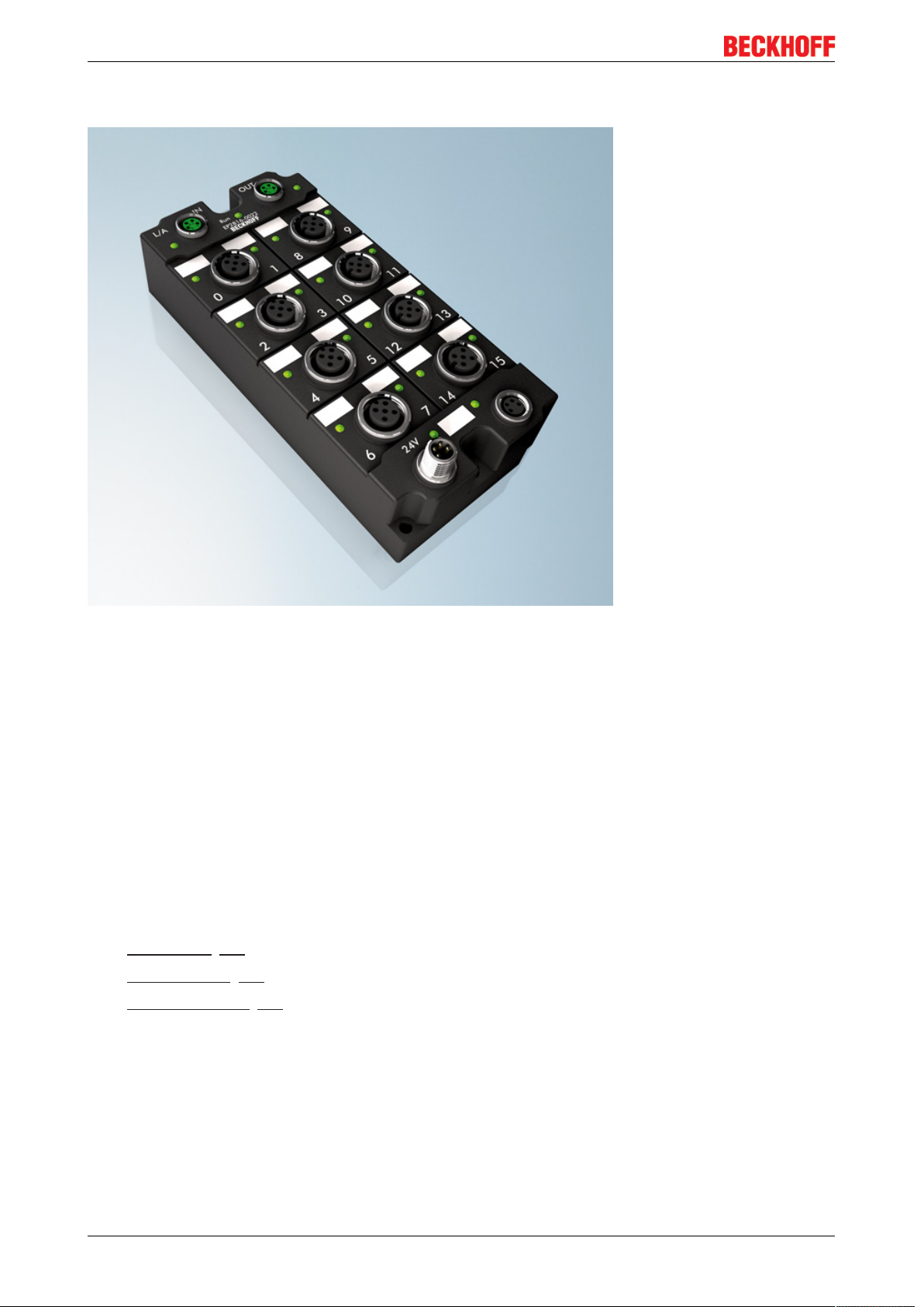
Fig.4: EP8309
EtherCAT Box with different digital and analog inputs and outputs
The EP8309-x022 EtherCAT Box has various digital and analog inputs and outputs.
The analog signals can be processed and output in the range 0/4…20mA, the digital signals in the range
24VDC.
The possible output currents are different and can be found in the technical data.
The resolution for the current signals takes place with 12bits, signed. This applies to input and output
signals.
The signal channels and the 24VDC supply have a common ground potential.
A PWMi output is integrated for connecting a proportional valve. For valves with integrated electronics, this
output can alternatively be operated as an analog current output with continuous 24V supply for the valve.
Quick links
• Installation [}27]
• Configuration [}48]
• UL requirements [}44]
EP8309-102210 Version: 2.0.0
Page 11

Product Overview
2.3 EP8309 - Technical data
Fieldbus
Technical Data EP8309-x022
Fieldbus EtherCAT
Fieldbus connection 2 x M8 socket (green)
Tacho inputs
Technical Data EP8309-x022
Number of tacho inputs 1 or 2 (dual-shaft mode or single-shaft mode)
Input type Single-shaft mode: two digital sensors on a
common axis
Dual-shaft mode: two digital sensors on two
different axes, no direction detection, no error
detection)
Tacho inputs connection [}41]
Rated input voltage 24VDC (-15%/+20%)
Input filter 2.5kHz
Signal voltage "0" -3...+5V (EN61131-2, type3)
Signal voltage "1" +11...+30V (EN61131-2, type3)
Input current typically 3mA (EN61131-2, type3)
Sensor supply from the control voltage Us
Current consumption of the sensors max. 0.5A, short-circuit-proof overall
M12
Digital inputs and outputs (DIO)
Technical Data EP8309-x022
Number of digital inputs and outputs (DIO) [}42]
Inputs
Input connections M12
Rated input voltage 24VDC (-15%/+20%)
Input filter 3.0ms
Signal voltage "0" -3...+5V (EN61131-2, type3)
Signal voltage "1" +11...+30V (EN61131-2, type3)
Input current typically 3mA (EN61131-2, type3)
Sensor supply from the control voltage Us
Current consumption of the sensors max. 0.5A, short-circuit-proof overall
Outputs
Output connections M12
Load type ohmic, inductive, lamp load
Rated output voltage 24VDC (-15%/+20%)
Output current max. 0.5A per channel for sockets 4 and 5
Short circuit current typically 1.5A
Output driver supply from load voltage Up
Output driver current consumption typically 8 mA per channel
8
max. 1.0A per channel for sockets 6 and 7
EP8309-1022 11Version: 2.0.0
Page 12

Product Overview
PWM outputs
Technical Data EP8309-x022
Number of PWM outputs (alternatively analog output) 1
Output connections [}43]
Load type ohmic/inductive > 1mH
Supply for the output stage 24VDC via power contacts
Output current per channel 1.2 A (short-circuit-proof, common thermal overload
PWM clock frequency approx. 30kHz
Rated load voltage 24VDC (-15%/+20%)
Resolution 10bit
Distributed Clocks yes
Analog inputs (AI)
Technical Data EP8309-x022
Number of analog inputs 2
Input connections [}42]
Signal type 0…20 mA or 4…20 mA (can be set for each CoE)
Input resistance 85 Ω typ. + diode voltage
Resolution 12bit (including sign)
Input filter limit frequency 5kHz
Conversion time approx. 100 µs
Measuring error < 0,3% (relative to full scale value)
M12
warning for both output stages)
M12 sockets
Analog outputs (AO)
Technical Data EP8309-x022
Number of analog outputs (alternatively PWMi output) 1
Output connections [}43]
Signal type 0…20 mA or 4…20 mA (can be set for each CoE)
Load <500Ω
Resolution 12bit
Conversion time approx. 40 µs
Measuring error < 0,3% (relative to full scale value)
M12 sockets
EP8309-102212 Version: 2.0.0
Page 13
Product Overview
General technical data
Technical Data EP8309-x022
Special features Multi-function module
Module electronic supply from the control voltage Us
Module electronic current consumption typically 120mA
Sensor supply from load voltage Up, DC, any value up to 30V
Actuator supply from load voltage Up, DC, any value up to 30V
Power supply connection Power supply: 1 x M8 plug, 4-pole
Onward connection: 1 x M8 socket, 4-pole
Process image Inputs: 2 x 16bit
Outputs: 2 x 16bit
Electrical isolation Control voltage/ fieldbus: 500V
Weight approx. 165g
Permissible ambient temperature during operation -25°C ... +60°C
Permissible ambient temperature during storage -40°C ... +85°C
Vibration/ shock resistance conforms to EN60068-2-6 / EN60068-2-27
EMC immunity/emission conforms to EN61000-6-2 / EN61000-6-4
Protection class IP65, IP66, IP67 (according to EN 60529)
Installation position variable
Approvals CE, cULus
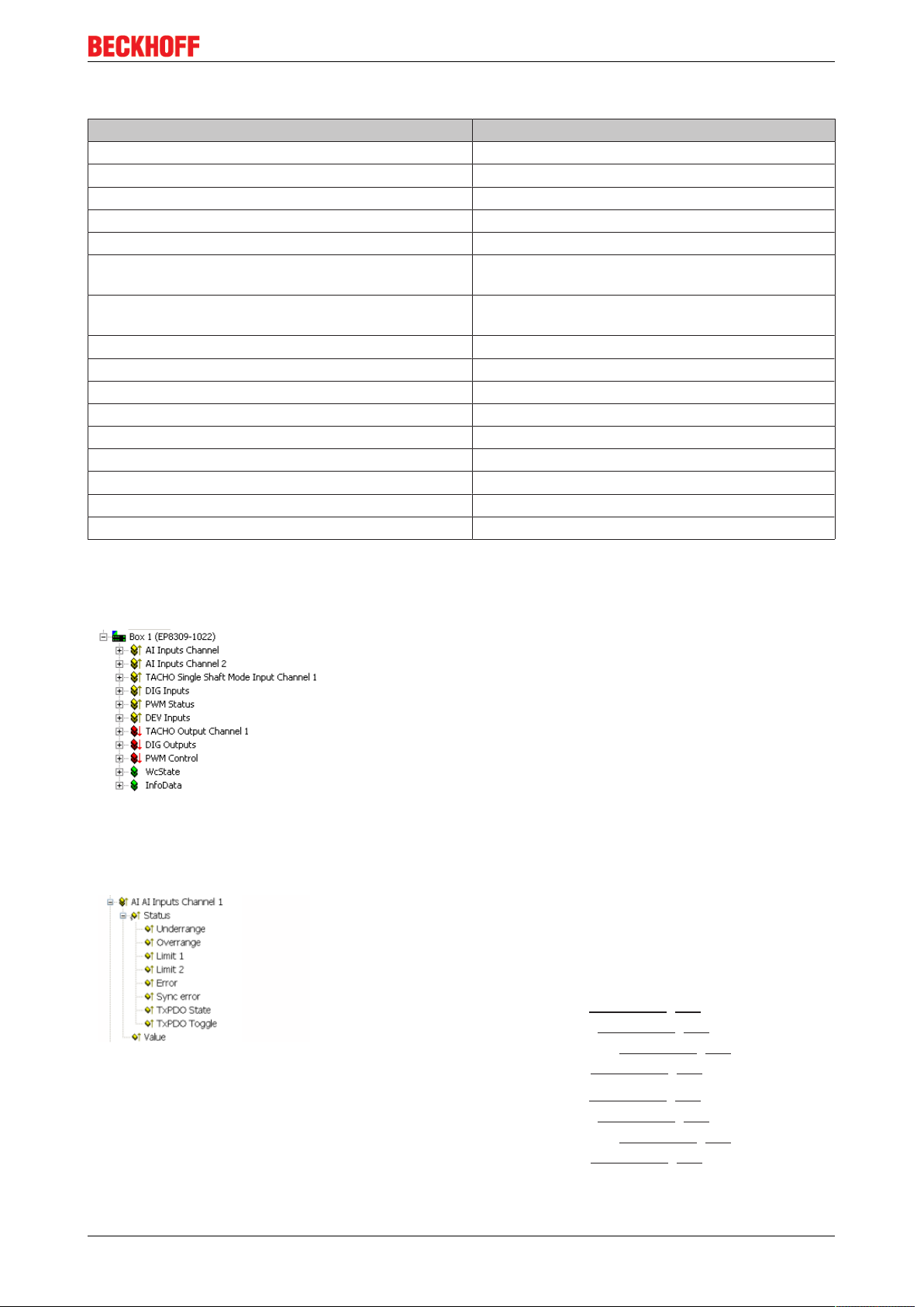
2.4 EP8309 - Process image
In the default setting the EP8309 is configured for:
• analog input channel 1
• analog input channel 2
• Tacho signal from two sensors on one axis (single-shaft mode)
• 6 digital inputs
• Status of PWM output
• Acknowledge / Reset in the event of a PWM error.
• 6 digital outputs
• General EtherCAT process data
AI Inputs Channel1 and 2
The data for the first analog channel can be found under AI Inputs
Channel1.
Underrange: Value of the analog input is less than 0/4mA or -10/0V
Overrange: Value of the analog input is greater than 20mA or +10V
Limit 1: with activated Limit 1 (object 0x8000:07 [}80]= 1) means
1:value less than limit 1 (set in object 0x8000:13 [}80])
2:value greater than limit 1 (set in object 0x8000:13 [}80])
3:value equal to limit 1 (set in object 0x8000:13 [}80])
Limit 2: with activated Limit 2 (object 0x8000:08 [}80]= 1) means
1:value less than limit 2 (set in object 0x8000:14 [}80])
2:value greater than limit 2 (set in object 0x8000:14 [}80])
3:value equal to limit 2 (set in object 0x8000:14 [}80])
Error: This bit is set if over- or under-range was detected.
EP8309-1022 13Version: 2.0.0
Page 14
Product Overview
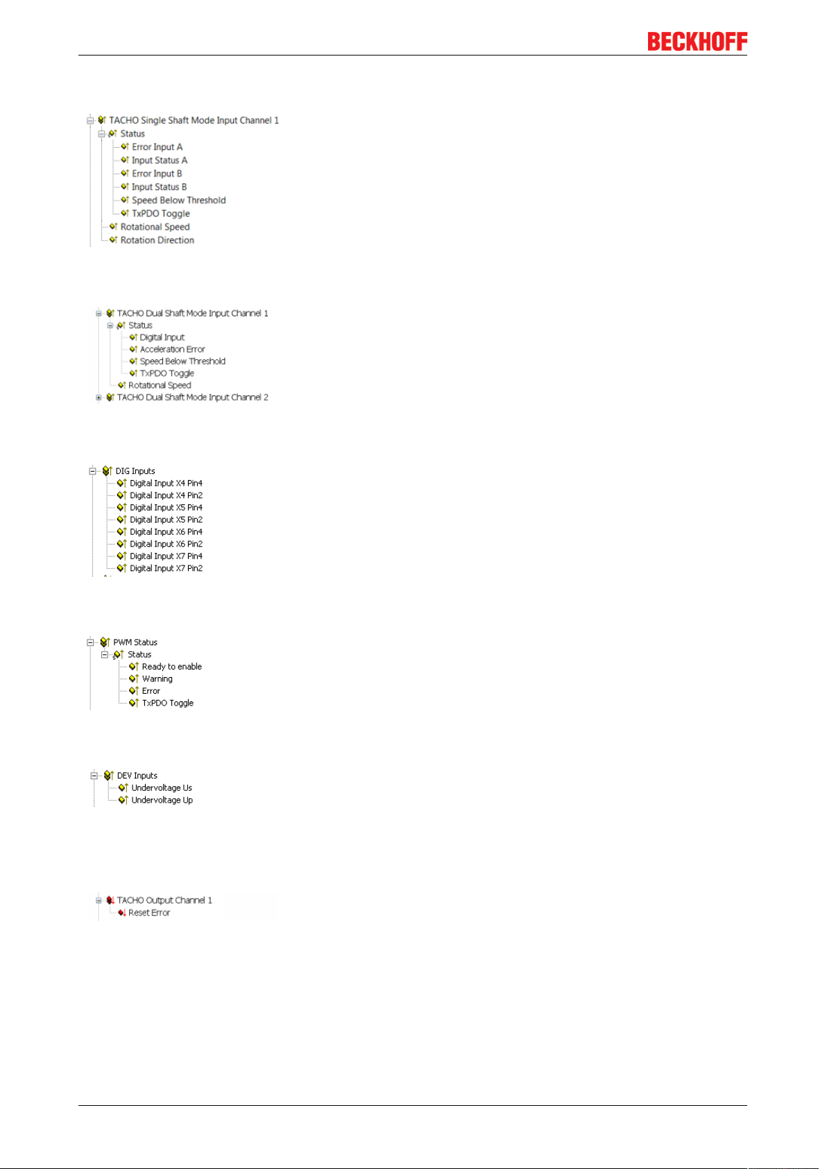
Tacho single-shaft mode (depending on the setting in the PDO assignment)
The data for the tacho input can be found under TACHO Single Shaft
Mode Input Channel 1.
see data under commissioning
Tacho dual-shaft mode (depending on the setting in the PDO assignment)
The data for the tacho input can be found under TACHO Dual Shaft
Mode Input Channel 1 or 2.
see data under commissioning
DIG Inputs
PWM Status
DEV Inputs
TACHO Output Channel 1
The data for the digital inputs can be found under DIG Inputs.
X4 Pin4 -> socket 4, pin 4
....
The data for the PWM output can be found under PWM Status
The diagnostic data for the two voltages Us and Up can be found under
DEV Inputs.
TRUE = voltage <= approx. 18 V
DC
....
The control data for the tacho input can be found under TACHO Output
Channel 1.
Reset Error - error reset
EP8309-102214 Version: 2.0.0
Page 15

Product Overview
DO Outputs
The data for the digital outputs can be found under DO Outputs.
X5 pin4 -> socket 5, pin 4
....
PWM control (activated through PDO assignment 0x1602, default PWM, alternatively AO)
The control data for the PWM output can be found under PWM Control.
Enable Dithering -> activate dithering
Enable -> activate PWM output
Reset -> reset on error
PWM output -> load-independent current, depending on module rating
(e.g. 1.2 A and setting in object 0x8060:10)
AO outputs (activated throughPDO assignment 0x1603), not activated by default
The values for the analog output can be found under AO Outputs.
Analog Output - output value
2.5 Pulse width modulation (PWM)
The Beckhoff terminals and box modules integrate compact PWM output stages in the smallest of designs.
PWM output stages control the output current through pulse width modulation (PWM) of the supply voltage.
This means that the full supply voltage is activated or deactivated at the output. The duty cycle (pulse width)
is modified, but not the voltage level. The current is built up based on the load connected to the inductance.
Fig.5: Operation at load with adequate inductance
Fig.6: Operation at load with inadequate inductance (near ohmic)
EP8309-1022 15Version: 2.0.0
Page 16

Product Overview
The figure Operation at load with inadequate inductance (virtually ohmic) illustrates operation with an
inadequate inductance. Continuous current flow is not reached. The current has "gaps". This mode of
operation is not permitted.
Pulse width current terminals require inductive loads
The load inductance should have a minimum inductance of 1 mH. Operation of the pulse
Note
width current terminals at loads with an inductance of less than 1 mH is not recommended,
since the intermittent current flow prevents reference between the set value and the arithmetic mean of the current.
2.6 Influencing of the PWMi output value by the
parameters
Fig.7: Influencing of the PWMi output value
EP8309-102216 Version: 2.0.0
Page 17

Basics of EtherCAT
3 Basics of EtherCAT
3.1 EtherCAT basics
Basic information on the EtherCAT fieldbus can be found in the EtherCAT system documentation.
3.2 Watchdog setting
General information on watchdog settings
The ELxxxx Terminals and EPxxxx Box Modules are equipped with a safety device (watchdog) that switches
the outputs to a safe state after a time that can be preset, for example in the case of interrupted process data
traffic, or to OFF, for example depending on device and setting.
The EtherCAT Slave Controller (ESC) has two watchdogs:
• SM watchdog (default: 100 ms)
• PDI watchdog (default: 100 ms)
SM Watchdog (SyncManagerWatchdog)
The SyncManager watchdog is reset after each successful EtherCAT process data communication with the
terminal/box. If no EtherCAT process data communication takes place with the terminal/box for longer than
the set and activated SM watchdog time, e.g. in the event of a line interruption, the watchdog is triggered and
the outputs are set to FALSE. The OP status of the terminal/box is unaffected by this. The watchdog is only
reset after a successful EtherCAT process data access. Set the monitoring time as specified below.
The SyncManager watchdog monitors correct and timely process data communication with the ESC from the
EtherCAT side.
PDI watchdog (process data watchdog)
If no PDI communication with the EtherCAT slave controller (ESC) takes place for longer than the set and
activated PDI watchdog time, this watchdog is triggered.
PDI (Process Data Interface) is the internal interface between the ESC and local processors in the EtherCAT
slave, for example. The PDI watchdog can be used to monitor this communication for failure.
The PDI watchdog monitors correct and timely process data communication with the ESC but from the
application side.
The SM and PDI watchdogs should be set separately for each slave in the TwinCAT System Manager:
EP8309-1022 17Version: 2.0.0
Page 18

Basics of EtherCAT
Fig.8: EtherCAT tab --> Advanced settings --> Behavior --> Watchdog
Comments:
• The multiplier applies to both watchdogs.
• Each watchdog has its own timer setting, which together with the multiplier results in a time.
• Important: The multiplier/timer setting is loaded into the slave on start-up, if the corresponding
checkbox is ticked. If the checkbox is not ticked, no download takes place, and the ESC setting
remains unchanged.
Multiplier
Both watchdogs receive their pulses from the local terminal/box clock, divided by the watchdog multiplier.
1/25 MHz * (watchdog multiplier + 2) = 100µs (for default setting of 2498 for the multiplier)
The standard setting of 1000 for the SM watchdog corresponds to a release time of 100 ms.
The value in multiplier + 2 corresponds to the number of basic 40ns ticks representing a watchdog tick.
The multiplier can be modified in order to adjust the watchdog time over a larger range.
Example "Set SM watchdog"
This checkbox enables manual setting of the watchdog times. If the outputs are set and the EtherCAT
communication is interrupted, the SM watchdog is triggered after the set time and the outputs are deleted.
This setting can be used for adapting a terminal to a slower EtherCAT master or long cycle times. The
default SM watchdog setting is 100 ms. The setting range is from 0 to 65535. Together with a multiplier in a
range from 1 to 65535, this covers a watchdog period of 0 to ~170 seconds.
Calculation
Multiplier = 2498 → watchdog base time = 1 / 25MHz * (2498 + 2) = 0.0001seconds = 100µs
SM watchdog = 10000 → 10000 * 100µs = 1second watchdog monitoring time
EP8309-102218 Version: 2.0.0
Page 19

CAUTION
CAUTION
Note
Basics of EtherCAT
Caution! Unintended behavior of the system is possible!
The function for switching off of the SM watchdog via SM watchdog = 0 is only implemented in terminals from version -0016. In previous versions this operating mode should
not be used.
Caution! Damage to the equipment and unintended behavior of the system is
possible!
If the SM watchdog is activated and a value of 0 is entered the watchdog switches off completely. This is watchdog deactivation! Outputs are then NOT set to a safe state, in the
event of an interruption in communication!
Outputs in SAFEOP
Watchdog monitoring is activated by default. It sets the outputs in the module to a safe
state (e.g. OFF), depending on the SAFEOP and OP settings, and depending on the device
and its settings. If this is prevented due to deactivation of watchdog monitoring in the module, outputs can be switched or remain set in device state SAFEOP.
EP8309-1022 19Version: 2.0.0
Page 20

Basics of EtherCAT
3.3 EtherCAT State Machine
The state of the EtherCAT slave is controlled via the EtherCAT State Machine (ESM). Depending upon the
state, different functions are accessible or executable in the EtherCAT slave. Specific commands must be
sent by the EtherCAT master to the device in each state, particularly during the bootup of the slave.
A distinction is made between the following states:
• Init
• Pre-Operational
• Safe-Operational and
• Operational
• Boot
The regular state of each EtherCAT slave after bootup is the OP state.
Fig.9: EtherCAT State Machine
Init
After switch-on the EtherCAT slave in the Init state. No mailbox or process data communication is possible.
The EtherCAT master initializes sync manager channels 0 and 1 for mailbox communication.
Pre-Operational (Pre-Op)
During the transition between Init and Pre-Op the EtherCAT slave checks whether the mailbox was initialized
correctly.
In Pre-Op state mailbox communication is possible, but not process data communication. The EtherCAT
master initializes the sync manager channels for process data (from sync manager channel 2), the FMMU
channels and, if the slave supports configurable mapping, PDO mapping or the sync manager PDO
assignment. In this state the settings for the process data transfer and perhaps terminal-specific parameters
that may differ from the default settings are also transferred.
Safe-Operational (Safe-Op)
During transition between Pre-Op and Safe-Op the EtherCAT slave checks whether the sync manager
channels for process data communication and, if required, the distributed clocks settings are correct. Before
it acknowledges the change of state, the EtherCAT slave copies current input data into the associated DPRAM areas of the EtherCAT slave controller (ECSC).
EP8309-102220 Version: 2.0.0
Page 21

Basics of EtherCAT
Mailbox and process data communication is possible in the Safe-Op state, but the slave keeps its outputs in
the safe state. However, the input data are cyclically updated.
Operational (Op)
Before the EtherCAT master switches the EtherCAT slave from Safe-Op to Op it must transfer valid output
data.
In the Op state the slave copies the output data of the masters to its outputs. Process data and mailbox
communication is possible.
Boot
In the Boot state the slave firmware can be updated. The Boot state can only be reached via the Init state.
In the Boot state mailbox communication via the file access over EtherCAT (FoE) protocol is possible, but no
other mailbox communication and no process data communication.
EP8309-1022 21Version: 2.0.0
Page 22

Basics of EtherCAT
3.4 CoE interface
General description
The CoE interface (CANopen over EtherCAT) is used for parameter management of EtherCAT devices.
EtherCAT slaves or the EtherCAT master manage fixed (read only) or variable parameters which they
require for operation, diagnostics or commissioning.
CoE parameters are arranged in a table hierarchy. In principle, the user has read access via the fieldbus.
The EtherCAT master (TwinCAT System Manager) can access the local CoE lists of the slaves via
EtherCAT in read or write mode, depending on the properties.
Different CoE parameter types are possible, including string (text), integer numbers, Boolean values or larger
byte fields. They can be used to describe a wide range of features. Examples of such parameters include
manufacturer ID, serial number, process data settings, device name, calibration values for analog
measurement or passwords.
Organization takes place on 2 levels by means of hexadecimal numbering: the (main) index is named first,
then the subindex. The value ranges are:
• Index 0 to 65535
• Subindex: 0…255
A parameter localized in this way is normally written as x8010:07, with preceding "x" to identify the
hexadecimal numerical range and a colon between index and subindex.
The relevant ranges for EtherCAT fieldbus users are:
• x1000: This is where fixed identity information for the device is stored, including name, manufacturer,
serial number etc., plus information about the current and available process data configurations.
• x8000: This is where the operational and functional parameters for all channels are stored, such as
filter settings or output frequency.
Other important ranges are:
• x4000: In some EtherCAT devices the channel parameters are stored here (as an alternative to the
x8000 range).
• x6000: Input PDOs ("input" from the perspective of the EtherCAT master)
• x7000: Output PDOs ("output" from the perspective of the EtherCAT master)
Availability
Not every EtherCAT device must have a CoE list. Simple I/O modules without dedicated
Note
If a device has a CoE list, it is shown in the TwinCAT System Manager as a separate tab with a listing of the
elements:
processor usually have no variable parameters and therefore no CoE list.
EP8309-102222 Version: 2.0.0
Page 23

Basics of EtherCAT
Fig.10: CoE-Online tab
The CoE objects from x1000 to x1600, which are available in the example device "EL2502", can be seen in
the above figure; the subindices from x1018 are expanded.
Data management
Some parameters, particularly the setting parameters of the slave, are configurable and writeable. This can
be done in write or read mode
• via the System Manager (figure above) by clicking. This is useful for commissioning of the system/
slaves. Click on the row of the index to be parameterized and enter a value in the SetValue dialog.
• from the control system/PLC via ADS, e.g. through function blocks from the TcEtherCAT.lib library This
is recommended for modifications while the system is running or if no System Manager or operating
staff are available.
Data management
If CoE parameters on the slave are changed online, this is saved fail-safe in the device
Note
Startup list
(EEPROM) in Beckhoff devices. This means that the changed CoE parameters are still retained after a restart. The situation may be different with other manufacturers.
Startup list
Changes in the local CoE list of the terminal are lost if the terminal is replaced. If a termi-
Note
nal is replaced with a new Beckhoff terminal, it will have the factory settings. It is therefore
advisable to link all changes in the CoE list of an EtherCAT slave with the Startup list of
the slave, which is processed whenever the EtherCAT fieldbus is started. In this way a replacement EtherCAT slave can automatically be parameterized with the specifications of
the user.
If EtherCAT slaves are used which are unable to store local CoE values permanently, the
Startup list must be used.
Recommended approach for manual modification of CoE parameters
• Make the required change in the System Manager. The values are stored locally in the EtherCAT slave
EP8309-1022 23Version: 2.0.0
Page 24

Basics of EtherCAT
• If the value is to be stored permanently, enter it in the Startup list. The order of the Startup entries is
usually irrelevant.
Fig.11: Startup list in the TwinCAT System Manager
The Startup list may already contain values that were configured by the System Manager based on the ESI
specifications. Additional application-specific entries can be created.
Online/offline directory
While working with the TwinCAT System Manager, a distinction has to be made whether the EtherCAT
device is "available", i.e. switched on and linked via EtherCAT and therefore online, or whether a
configuration is created offline without connected slaves.
In both cases a CoE directory is visible according to the figure "CoE-Online tab", but the connectivity is
displayed as offline/online.
If the slave is offline
• the offline list from the ESI file is displayed. In this case modifications are not meaningful or possible.
• the configured status is shown under Identity
• no firmware or hardware version is displayed, since these are features of the physical device.
• Offline is shown in red
EP8309-102224 Version: 2.0.0
Page 25

Basics of EtherCAT
Fig.12: Offline list
If the slave is online
• the actual current slave directory is read. This may take several seconds, depending on the size and
cycle time.
• the actual identity is displayed
• the firmware and hardware version of the equipment according to the electronic information is
displayed.
• Online is shown in green
Fig.13: Online list
EP8309-1022 25Version: 2.0.0
Page 26

Basics of EtherCAT
Channel-based order
The CoE directory is located in EtherCAT devices that usually encompass several functionally equivalent
channels. e.g. a 4-channel 0 – 10 V analog input terminal also has 4 logical channels and thus 4 identical
sets of parameter data for the channels. In order to avoid having to list each channel in the documentation,
the placeholder "n" tends to be used for the individual channel numbers.
In the CoE system 16 indices, each with 255 subindices, are generally sufficient for representing all channel
parameters. The channel-based order is therefore arranged in 16
dec
/10
steps. The parameter range x8000
hex
exemplifies this:
• Channel 0: parameter range x8000:00 ... x800F:255
• Channel 1: parameter range x8010:00 ... x801F:255
• Channel 2: parameter range x8020:00 ... x802F:255
• …
This is generally written as x80n0. Detailed information on the CoE interface can be found in the EtherCAT
system documentation on the Beckhoff website.
EP8309-102226 Version: 2.0.0
Page 27

4 Mounting and cabling
4.1 Mounting
4.1.1 Dimensions
Mounting and cabling
Fig.14: Dimensions of the EtherCAT Box Modules
All dimensions are given in millimeters.
Housing properties
EtherCAT Box lean body wide body
Housing material PA6 (polyamide)
Casting compound Polyurethane
Mounting two fastening holes Ø3mm for M3 two fastening holes Ø3mm for M3
two fastening holes Ø4,5mm for M4
Metal parts Brass, nickel-plated
Contacts CuZn, gold-plated
Power feed through max. 4A
Installation position variable
Protection class IP65, IP66, IP67 (conforms to EN 60529) when screwed together
Dimensions (HxWxD) ca. 126 x 30 x 26,5mm ca. 126 x 60 x 26,5mm
Weight approx. 125g, depending on module type approx. 250g, depending on module
type
EP8309-1022 27Version: 2.0.0
Page 28
Mounting and cabling
4.1.2 Fixing
Note or pointer
While mounting the modules, protect all connectors, especially the IP-Link, against contam-
Note
Modules with narrow housing are mounted with two M3 bolts.
Modules with wide housing are mounted with two M3 bolts to the fixing holes located at the corners or
mounted with two M4 bolts to the fixing holes located centrally.
The bolts must be longer than 15 mm. The fixing holes of the modules are not threaded.
When assembling, remember that the fieldbus connectors increases the overall height. See chapter
accessories.
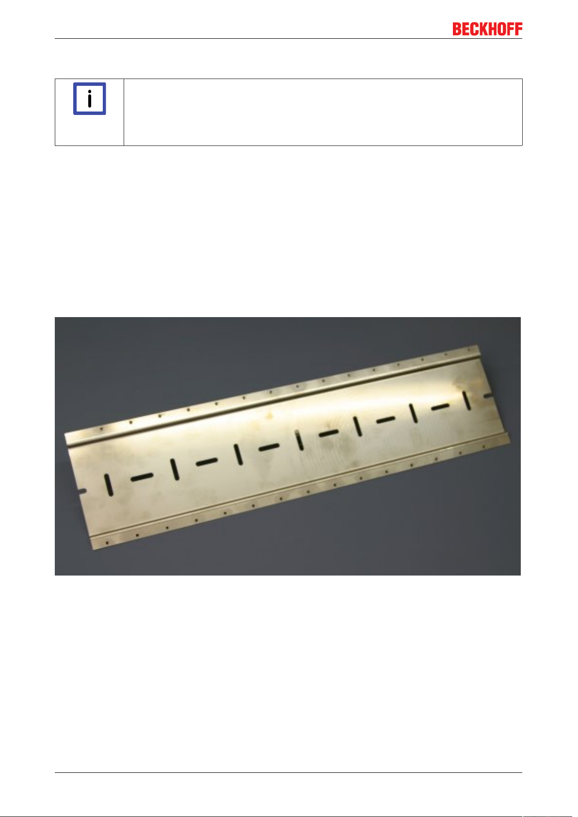
Mounting Rail ZS5300-0001
The mounting rail ZS5300-0001 (500 mm x 129 mm) allows the time saving assembly of modules.
The rail is made of stainless steel, 1.5 mm thick, with already pre-made M3 threads for the modules. The rail
has got 5.3 mm slots to mount it via M5 screws to the machine.
ination! Only with connected cables or plugs the protection class IP67 is guaranteed! Unused connectors have to be protected with the right plugs! See for plug sets in the catalogue.
Fig.15: Mounting Rail ZS5300-000
The mounting rail is 500 mm long, that way 15 narrow modules can be mounted with a distance of 2 mm
between two modules. The rail can be cut to length for the application.
Mounting Rail ZS5300-0011
The mounting rail ZS5300-0011 (500 mm x 129 mm) has in addition to the M3 treads also pre-made M4
treads to fix 60 mm wide modules via their middle holes.
Up to 14 narrow or 7 wide modules may be mixed mounted.
EP8309-102228 Version: 2.0.0
Page 29

Mounting and cabling
4.2 Cabling
4.2.1 Connections
The EP8309 has different signals that can be connected via the eight M12 sockets.
Comment Connector Comment
EtherCAT IN EtherCAT OUT
Socket 1:
• analog In
Socket 2:
• analog In
Socket 3:
• digital In channel 1 / Tacho
input 1
• digital In channel 2 / Tacho
input 2
Socket 4:
• digital In/Out channel3
• digital In/Out channel4
Power In Power Out
Socket 5:
• digital In/Out channel1
• digital In/Out channel2
Socket 6:
• digital In/Out channel1
• digital In/Out channel2
Socket 7:
• digital In/Out channel3
• digital In/Out channel4
Socket 8:
• pulse width current output
or
• analog output
EP8309-1022 29Version: 2.0.0
Page 30
Mounting and cabling
4.2.2 Nut torque for connectors
M8 connectors
It is recommended to pull the M8 connectors tight with a nut torque of 0.4 Nm. When using the torque control
screwdriver ZB8800 is also a max. torque of 0.5Nm permissible.
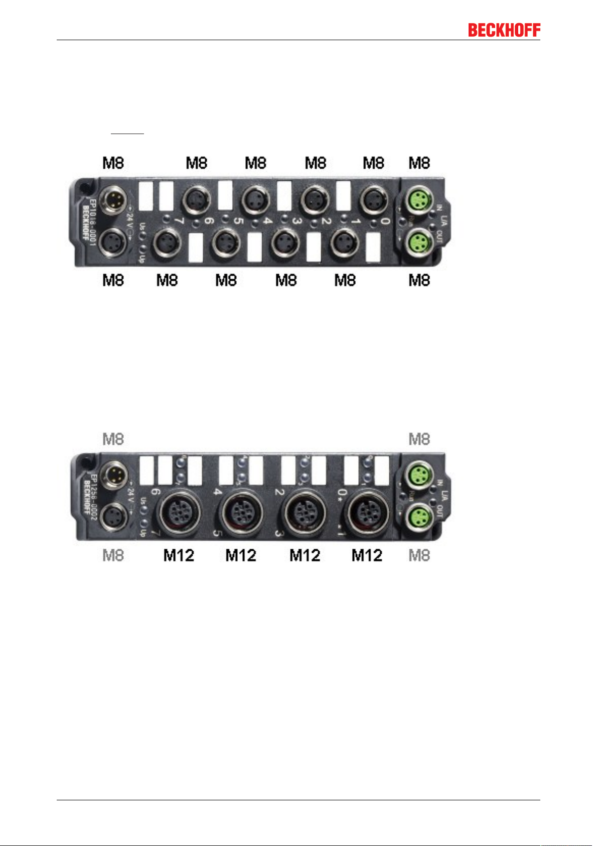
Fig.16: EtherCAT Box with M8 connectors
M12 connectors
It is recommended to pull the M12 connectors tight with a nut torque of 0.6 Nm.
Fig.17: EtherCAT Box with M8 and M12 connectors
EP8309-102230 Version: 2.0.0
Page 31

7/8" plug connectors
We recommend fastening the 7/8" plug connectors with a torque of 1.5Nm.
Fig.18: 7/8" plug connectors
Torque socket wrenches
Mounting and cabling
Fig.19: ZB8801 torque socket wrench
Ensure the right torque
Use the torque socket wrenches available by Beckhoff to pull the connectors tight (ZB8800,
Note
ZB8801-0000)!
EP8309-1022 31Version: 2.0.0
Page 32

Mounting and cabling
4.2.3 EtherCAT
4.2.3.1 EtherCAT connection
For the incoming and ongoing EtherCAT connection,
• the EtherCAT Box (EPxxxx) has two M8 sockets, marked in green
• the Coupler Box (FBB-x110) has two M12 sockets
Fig.20: EtherCAT Box: M8 (30mm housing)
Fig.21: EtherCAT Box: M8 60mm housing (EP9214 for example )
EP8309-102232 Version: 2.0.0
Page 33

Mounting and cabling
Fig.22: Coupler Box: M12
Assignment
There are various different standards for the assignment and colors of connectors and cables for Ethernet/
EtherCAT.
Ethernet/EtherCAT Plug connector Cable Standard
Signal Description M8 M12 RJ45
Tx + Transmit Data+ Pin 1 Pin 1 Pin 1 yellow
Tx - Transmit Data- Pin 4 Pin 3 Pin 2 orange
Rx + Receive Data+ Pin 2 Pin 2 Pin 3 white
Rx - Receive Data- Pin 3 Pin 4 Pin 6 blue
1
ZB9010, ZB9020,
ZB9030, ZB9032,
ZK1090-6292,
ZK1090-3xxx-xxxx
2
2
2
2
ZB9031 and old
versions
of ZB9030, ZB9032,
ZK1090-3xxx-xxxx
orange/white
orange
blue/white
3
blue
3
3
3
TIA-568B
white/orange
orange
white/green
green
Shield Shield Housing Shroud Screen Screen Screen
1
) colored markings according to EN 61918 in the four-pin RJ45 connector ZS1090-0003
2
) wire colors according to EN 61918
3
) wire colors
Assimilation of color coding for cable ZB9030, ZB9032 and ZK1090-3xxxxxxxx (with M8 connectors)
Note
For unification the prevalent cables ZB9030, ZB9032 and ZK1090-3xxx-xxxx this means
the pre assembled cables with M8 connectors were changed to the colors of EN61918 (yellow, orange, white, blue).So different color coding exists. But the electrical properties are
absolutely identical.
EtherCAT connectors
The following connectors can be supplied for use in Beckhoff EtherCAT systems.
EP8309-1022 33Version: 2.0.0
Page 34

Mounting and cabling
Designation Plug connector Comment
ZS1090-0003 RJ45 four-pin, IP20, for field assembly
ZS1090-0004 M12 four-pin, IP67, for field assembly
ZS1090-0005 RJ45 eight-pin, IP20, for field assembly, suitable for GigaBit Ethernet
ZS1090-0006 M8 male four-pin, IP67, for field assembly, for ZB903x cable
ZS1090-0007 M8 female four-pin, IP67, for field assembly, for ZB903x cable
ZS1090-1006 M8 male four-pin, IP67, for field assembly up to OD = 6.5mm
ZS1090-1007 M8 female four-pin, IP67, for field assembly up to OD = 6.5mm
4.2.3.2 EtherCAT - Fieldbus LEDs
Fig.23: EtherCAT-LEDs
LED display
LED Display Meaning
IN L/A off no connection to the preceding EtherCAT module
Lit LINK: connection to the preceding EtherCAT module
flashing ACT: Communication with the preceding EtherCAT module
OUT L/A off no connection to the following EtherCAT module
Lit LINK: connection to the following EtherCAT module
flashing ACT: Communication with the following EtherCAT module
Run off Status of the EtherCAT module is Init
flashes quickly Status of the EtherCAT module is pre-operational
flashes slowly Status of the EtherCAT module is safe-operational
Lit Status of the EtherCAT module is operational
EtherCAT statuses
The various statuses in which an EtherCAT module may be found are described in the Ba-
Note
sic System Documentation for EtherCAT, which is available for download from our website
(www.beckhoff.com) under Downloads.
EP8309-102234 Version: 2.0.0
Page 35

Mounting and cabling
4.2.4 Power Connection
4.2.4.1 Power Connection
The feeding and forwarding of supply voltages is done via two M8 connectors at the bottom end of the
modules:
• IN: left M8 connector for feeding the supply voltages
• OUT: right M8 connector for forwarding the supply voltages
Fig.24: EtherCAT Box, Connectors for power supply
Fig.25: Pin assignment M8, Power In and Power Out
Table1: PIN assignment
Pin Voltage
1 Control voltage Us, +24V
2 Auxiliary voltage Up, +24V
DC
DC
3 GNDs* *) may be connected internally to each other depending on the module: see specific
4 GNDp*
module descriptions
The pins M8 connectors carry a maximum current of 4A.
Two LEDs display the status of the supply voltages.
Don't confuse the power connectors with the EtherCAT connectors!
Never connect the power cables (M8, 24VDC) with the green marked EtherCAT sockets of
Attention
the EtherCAT Box Modules! This can damage the modules!
Control voltage Us: 24V
DC
Power is supplied to the fieldbus, the processor logic, the inputs and the sensors from the 24VDC control
voltage Us. The control voltage is electrically isolated from the fieldbus circuitry.
EP8309-1022 35Version: 2.0.0
Page 36

Mounting and cabling
Auxiliary voltage Up 24V
DC
The Auxiliary voltage Up supplies the digital outputs; it can be brought in separately. If the load voltage is
switched off, the fieldbus functions and the power supply and functionality of the inputs are retained.
Redirection of the supply voltages
The IN and OUT power connections are bridged in the module (not IP204x-Bxxx and IE204x). The supply
voltages Us and Up can thus easily be transferred from EtherCATBox to EtherCATBox.
Pay attention to the maximum permissible current!
Pay attention also for the redirection of the supply voltages Us and Up, the maximum per-
Attention
missible current for M8 connectors of 4A must not be exceeded!
EP8309-102236 Version: 2.0.0
Page 37

Mounting and cabling
Supply via EP92x4-0023 PowerBox modules
If the machine requires higher current or if the EtherCAT Box Modules are installed far away from the control
cabinet with included power supply, the usage of four cannel power distribution modules EP9214 or EP9224
(with integrated data logging, see www.beckhoff.com/EP9224) is recommended.
With these modules intelligent power distribution concepts with up to 2x16A and a maximum of 2.5mm²
cable cross-section can be realized.
Fig.26: EP92x4-0023, Connectors for Power In and Power Out
Fig.27: Pin assignment 7/8”, Power In and Power Out
EP8309-1022 37Version: 2.0.0
Page 38

Mounting and cabling
Electrical isolation
Digital modules
In the digital input/output modules, the grounds of the control voltage (GNDs) and the auxiliary voltage
(GNDp) are connected to each other!
Check this at the documentation of each used EtherCAT Box.
Analog modules
In the analog input/output modules the grounds of the control voltage (GNDs) and the auxiliary voltage
(GNDp) are separated from each other in order to ensure electrical isolation of the analog signals from the
control voltage.
In some of the analog modules the sensors or actuators are supplied by Up - this means, for instance, that in
the case of 0...10 V inputs, any reference voltage (0...30 V) may be connected to Up; this is then available to
the sensors (e.g. smoothed 10 V for measuring potentiometers).
Details of the power supply may be taken from the specific module descriptions.
Electrical isolation may be cancelled!
If digital and analog fieldbus boxes are connected directly via four-core power leads, the
Attention
analog signals in the fieldbus boxes may be no longer electrically isolated from the control
voltage!
4.2.4.2 Status LEDs for power supply
Fig.28: Status LEDs for power supply
LED display
LED Display Meaning
Us (Control voltage) off The power supply voltage Us is not present
green illuminated The power supply voltage Us is present
red illuminated Because of overload (current>0.5A) the sensor supply
generated from power supply voltage Us was switched off for
all sensors fed from this.
Up (Auxiliary voltage) off The power supply voltage Up is not present
green illuminated The power supply voltage Up is present
EP8309-102238 Version: 2.0.0
Page 39

4.2.4.3 Power cable
Ordering data
Mounting and cabling
Order identifier Power cable Screw
Contacts Cross-section Length
connector
ZK2020-3200-0020 Straight socket, open
ZK2020-3200-0050 5.00m
end
M8 4-pole 0.34 mm
2
2.00m
ZK2020-3200-0100 10.00m
ZK2020-3400-0020 Angled socket, open
ZK2020-3400-0050 5.00m
end
2.00m
ZK2020-3400-0100 10.00m
ZK2020-3132-0001 Straight socket,
ZK2020-3132-0005 0.50m
straight connector
0.15m
ZK2020-3132-0010 1.00m
ZK2020-3132-0020 2.00m
ZK2020-3132-0050 5.00m
ZK2020-3334-0001 Angled socket, angled
ZK2020-3334-0005 0.50m
connector
0.15m
ZK2020-3334-0010 1.00m
ZK2020-3334-0020 2.00m
ZK2020-3334-0050 5.00m
Further available power cables and the associated data sheets can be found in the Beckhoff catalogue or on
our website (http://www.beckhoff.de).
Technical Data
Data
Rated voltage according to IEC61076-2-101 30V
DC
Contamination level according to IEC 60 664-1 3/2
Insulation resistance IEC 60 512-2 >109 Ω
Current carrying capacity according to IEC 60512-3 4A
Volume resistance according to IEC 60512-2 < 5mΩ
Protection class conforms to IEC 60529 IP65/66/67, when screwed together
Ambient temperature -30 °C to +80 °C
4.2.4.4 Power cable conductor losses M8
The ZK2020-xxxx-yyyy power cables should not exceed the total length of 15m at 4A (with continuation).
When planning the cabling, note that at 24V nominal voltage, the functionality of the module can no longer
be assured if the voltage drop reaches 6V. Variations in the output voltage from the power supply unit must
also be taken into account.
EP8309-1022 39Version: 2.0.0
Page 40

Mounting and cabling
Fig.29: Power cable conductor losses
Example
8m power cable with 0.34mm² cross-section has a voltage drop of 3.2V at 4A.
EP92x4 Power Distribution Modules
With EP9214 and EP9224 Power Distribution Modules intelligent concepts for voltage sup-
Note
ply are available. Further information may be found under www.beckhoff.com/EP9224.
EP8309-102240 Version: 2.0.0
Page 41

Mounting and cabling
4.2.5 Signal connection
4.2.5.1 Digital inputs M12
The digital input modules acquire the binary control signals from the process level and transmit them to the
higher-level automation device.
The signals are connected via M12 connectors.
Fig.30: Digital inputs M12
The sensors are supplied with a common maximum current of 0.5Afrom the control voltage Us.
Light emitting diodes indicate the signal state of the inputs.
EP8309-1022 41Version: 2.0.0
Page 42

Mounting and cabling
4.2.5.2 Digital inputs/outputs M12
The digital input/output channels connect the binary control signals from the automation device for the
process level with the actuators or read digital input signals.
No configuration is required. For each channel one input or output can be connected.
If an output is used, the change in status can be verified on switch-on via the corresponding signal in the
input process image.
The signals are connected via M12 connectors.
Fig.31: Digital inputs/outputs M12
The outputs are short-circuit proof and protected against inverse connection.
LEDs indicate the signal state of the outputs.
4.2.5.3 Analog inputs M12
The analog signal inputs pick up analog control signals from the process level and transmit them to the
higher-level automation device.
The signals are connected via M12 connectors.
Fig.32: Analog inputs M12
The sensors are supplied with a common maximum current of 0.5Afrom the control voltage Us.
LEDs indicate the status of the inputs.
EP8309-102242 Version: 2.0.0
Page 43

Mounting and cabling
4.2.5.4 Analog output and PWMi output M12
Via the multi-function output either an analog output or a PWMi output can be output to a proportional valve,
for example.
The signals are connected via M12 connectors.
Fig.33: Analog output and PWMi output M12
The outputs are short-circuit-proof.
LEDs indicate the signal state of the output.
4.2.5.5 Status LEDs
Fig.34: Status LEDs
Status LEDs at the M12 connections
Connection LED Display Meaning
M12 socket analog
inputs, PWMi
Correct function is indicated if the green Run LED is on and the red Error LED is off.
left off No data transfer to the D/A converter
green Data transfer to the D/A converter
right off Function OK
red Analog error: broken wire or measured value outside the
measuring range
PWMi: general error, see status word
Status LEDs at the M12 connections
Connection LED Display Meaning
M12 socket digital
inputs/outputs
EP8309-1022 43Version: 2.0.0
left /
right
off Input / output off or Low
green Input / output on or High
Page 44

Mounting and cabling
4.2.6 UL Requirements
The installation of the EtherCAT Box Modules certified by UL has to meet the following requirements.
Supply voltage
CAUTION!
This UL requirements are valid for all supply voltages of all marked EtherCAT Box Mod-
CAUTION
CAUTION
ules!
For the compliance of the UL requirements the EtherCAT Box Modules should only be supplied
• by a 24 VDC supply voltage, supplied by an isolating source and protected by means of
a fuse (in accordance with UL248), rated maximum 4 Amp, or
• by a 24 VDC power source, that has to satisfy NEC class 2.
A NEC class 2 power supply shall not be connected in series or parallel with another
(class 2) power source!
CAUTION!
To meet the UL requirements, the EtherCAT Box Modules must not be connected to unlimited power sources!
Networks
CAUTION!
To meet the UL requirements, EtherCAT Box Modules must not be connected to telecom-
CAUTION
Ambient temperature range
munication networks!
CAUTION!
To meet the UL requirements, EtherCAT Box Modules has to be operated only at an ambi-
CAUTION
Marking for UL
All EtherCAT Box Modules certified by UL (Underwriters Laboratories) are marked with the following label.
Fig.35: UL label
ent temperature range of 0 to 55°C!
EP8309-102244 Version: 2.0.0
Page 45

Commissioning and Configuration
5 Commissioning and Configuration
5.1 Inserting into the EtherCAT network
Installation of the latest XML device description
Please ensure that you have installed the latest XML device description in TwinCAT. This
Note
At the Beckhoff TwinCAT System Manager the configuration tree can be build in two different ways:
• by scanning [}45] for existing hardware (called "online") and
• by manual inserting/appending [}45] of fieldbus devices, couplers and slaves.
Automatic scanning in of the box
• The EtherCAT system must be in a safe, de-energized state before the EtherCAT modules are
connected to the EtherCAT network!
• Switch on the operating voltage, open the TwinCAT System Manager [}48] (Config mode), and scan
in the devices (see Fig. 1). Acknowledge all dialogs with "OK", so that the configuration is in "FreeRun"
mode.
can be downloaded from the Beckhoff website (http://www.beckhoff.de/english/download/
elconfg.htm?id=1983920606140) and installed according to the installation instructions.
Fig.36: Scanning in the configuration (I/O Devices -> right-click -> Scan Devices...)
Appending a module manually
• The EtherCAT system must be in a safe, de-energized state before the EtherCAT modules are
connected to the EtherCAT network!
• Switch on the operating voltage, open the TwinCAT System Manager [}48] (Config mode)
• Append a new I/O device. In the dialog that appears select the device EtherCAT (Direct Mode), and
confirm with OK.
EP8309-1022 45Version: 2.0.0
Page 46

Commissioning and Configuration
Fig.37: Appending a new I/O device (I/O Devices -> right-click -> Append Device...)
Fig.38: Selecting the device EtherCAT
• Append a new box.
Fig.39: Appending a new box (Device -> right-click -> Append Box...)
• In the dialog that appears select the desired box (e.g. EP2816-0008), and confirm with OK.
EP8309-102246 Version: 2.0.0
Page 47

Commissioning and Configuration
Fig.40: Selecting a Box (e.g. EP2816-0008)
Fig.41: Appended Box in the TwinCAT tree
EP8309-1022 47Version: 2.0.0
Page 48

Commissioning and Configuration
5.2 Configuration via TwinCAT
In the left-hand window of the TwinCAT System Manager, click on the branch of the EtherCAT Box you wish
to configure (EP2816-0008 in this example).
Fig.42: Branch of the EtherCAT box to be configured
In the right-hand window of the TwinCAT System manager, various tabs are now available for configuring
the EtherCAT Box.
General tab
Fig.43: General tab
Name Name of the EtherCAT device
Id Number of the EtherCAT device
Type EtherCAT device type
Comment Here you can add a comment (e.g. regarding the system).
Disabled Here you can deactivate the EtherCAT device.
Create symbols Access to this EtherCAT slave via ADS is only available if this checkbox is
activated.
EP8309-102248 Version: 2.0.0
Page 49

Commissioning and Configuration
EtherCAT tab
Fig.44: EtherCAT tab
Type EtherCAT device type
Product/Revision Product and revision number of the EtherCAT device
Auto Inc Addr. Auto increment address of the EtherCAT device. The auto increment address can
be used for addressing each EtherCAT device in the communication ring through
its physical position. Auto increment addressing is used during the start-up phase
when the EtherCAT master allocates addresses to the EtherCAT devices. With
auto increment addressing the first EtherCAT slave in the ring has the address
0000
. For each further slave the address is decremented by 1 (FFFF
hex
, FFFE
hex
etc.).
EtherCAT Addr. Fixed address of an EtherCAT slave. This address is allocated by the EtherCAT
master during the start-up phase. Tick the checkbox to the left of the input field in
order to modify the default value.
Previous Port Name and port of the EtherCAT device to which this device is connected. If it is
possible to connect this device with another one without changing the order of the
EtherCAT devices in the communication ring, then this combobox is activated and
the EtherCAT device to which this device is to be connected can be selected.
Advanced Settings This button opens the dialogs for advanced settings.
hex
The link at the bottom of the tab points to the product page for this EtherCAT device on the web.
Process Data tab
Indicates the configuration of the process data. The input and output data of the EtherCAT slave are
represented as CANopen process data objects (PDO). The user can select a PDO via PDO assignment and
modify the content of the individual PDO via this dialog, if the EtherCAT slave supports this function.
EP8309-1022 49Version: 2.0.0
Page 50

Commissioning and Configuration
Fig.45: Process Data tab
Sync Manager
Lists the configuration of the Sync Manager (SM).
If the EtherCAT device has a mailbox, SM0 is used for the mailbox output (MbxOut) and SM1 for the mailbox
input (MbxIn).
SM2 is used for the output process data (outputs) and SM3 (inputs) for the input process data.
If an input is selected, the corresponding PDO assignment is displayed in the PDO Assignment list below.
PDO Assignment
PDO assignment of the selected Sync Manager. All PDOs defined for this Sync Manager type are listed
here:
• If the output Sync Manager (outputs) is selected in the Sync Manager list, all RxPDOs are displayed.
• If the input Sync Manager (inputs) is selected in the Sync Manager list, all TxPDOs are displayed.
The selected entries are the PDOs involved in the process data transfer. In the tree diagram of the System
Manager these PDOs are displayed as variables of the EtherCAT device. The name of the variable is
identical to the Name parameter of the PDO, as displayed in the PDO list. If an entry in the PDO assignment
list is deactivated (not selected and greyed out), this indicates that the input is excluded from the PDO
assignment. In order to be able do select a greyed out PDO, the currently selected PDO has to be
deselected first.
EP8309-102250 Version: 2.0.0
Page 51

Commissioning and Configuration
Activation of PDO assignment
• the EtherCAT slave has to run through the PS status transition cycle (from pre-opera-
Note
PDO list
List of all PDOs supported by this EtherCAT device. The content of the selected PDOs is displayed in the
PDO Content list. The PDO configuration can be modified by double-clicking on an entry.
Column Description
Index PDO index.
Size Size of the PDO in bytes.
Name Name of the PDO.
If this PDO is assigned to a Sync Manager, it appears as a variable of the slave with this
parameter as the name.
Flags F Fixed content: The content of this PDO is fixed and cannot be changed by the System
M Mandatory PDO. This PDO is mandatory and must therefore be assigned to a Sync
SM Sync Manager to which this PDO is assigned. If this entry is empty, this PDO does not take part
in the process data traffic.
SU Sync unit to which this PDO is assigned.
tional to safe-operational) once (see Online tab [}54]),
• and the System Manager has to reload the EtherCAT slaves ( button)
Manager.
Manager! Consequently, this PDO cannot be deleted from the PDO Assignment list
PDO Content
Indicates the content of the PDO. If flag F (fixed content) of the PDO is not set the content can be modified.
Download
If the device is intelligent and has a mailbox, the configuration of the PDO and the PDO assignments can be
downloaded to the device. This is an optional feature that is not supported by all EtherCAT slaves.
PDO Assignment
If this check box is selected, the PDO assignment that is configured in the PDO Assignment list is
downloaded to the device on startup. The required commands to be sent to the device can be viewed in the
Startup [}51] tab.
PDO Configuration
If this check box is selected, the configuration of the respective PDOs (as shown in the PDO list and the
PDO Content display) is downloaded to the EtherCAT slave.
Startup tab
The Startup tab is displayed if the EtherCAT slave has a mailbox and supports the CANopen over EtherCAT
(CoE) or Servo drive over EtherCAT protocol. This tab indicates which download requests are sent to the
mailbox during startup. It is also possible to add new mailbox requests to the list display. The download
requests are sent to the slave in the same order as they are shown in the list.
EP8309-1022 51Version: 2.0.0
Page 52

Commissioning and Configuration
Fig.46: Startup tab
Column Description
Transition Transition to which the request is sent. This can either be
• the transition from pre-operational to safe-operational (PS), or
• the transition from safe-operational to operational (SO).
If the transition is enclosed in "<>" (e.g. <PS>), the mailbox request is fixed and cannot be
modified or deleted by the user.
Protocol Type of mailbox protocol
Index Index of the object
Data Date on which this object is to be downloaded.
Comment Description of the request to be sent to the mailbox
Move Up This button moves the selected request up by one position in the list.
Move Down This button moves the selected request down by one position in the list.
New This button adds a new mailbox download request to be sent during startup.
Delete This button deletes the selected entry.
Edit This button edits an existing request.
CoE - Online tab
The additional CoE - Online tab is displayed if the EtherCAT slave supports the CANopen over EtherCAT
(CoE) protocol. This dialog lists the content of the object directory of the slave (SDO upload) and enables the
user to modify the content of an object from this list. Details for the objects of the individual EtherCAT
devices can be found in the device-specific object descriptions.
EP8309-102252 Version: 2.0.0
Page 53

Commissioning and Configuration
Fig.47: CoE - Online tab
Object list display
Column Description
Index Index and subindex of the object
Name Name of the object
Flags RW The object can be read, and data can be written to the object (read/write)
RO The object can be read, but no data can be written to the object (read only)
P An additional P identifies the object as a process data object.
Value Value of the object
Update List The Update list button updates all objects in the displayed list
Auto Update If this check box is selected, the content of the objects is updated automatically.
Advanced The Advanced button opens the Advanced Settings dialog. Here you can specify which
objects are displayed in the list.
EP8309-1022 53Version: 2.0.0
Page 54

Commissioning and Configuration
Fig.48: Advanced settings
Online
- via SDO information
Offline
- via EDS file
Online tab
If this option button is selected, the list of the objects included in the object
directory of the slave is uploaded from the slave via SDO information. The list
below can be used to specify which object types are to be uploaded.
If this option button is selected, the list of the objects included in the object
directory is read from an EDS file provided by the user.
Fig.49: Online tab
EP8309-102254 Version: 2.0.0
Page 55

Commissioning and Configuration
State Machine
Init This button attempts to set the EtherCAT device to the Init state.
Pre-Op This button attempts to set the EtherCAT device to the pre-operational state.
Op This button attempts to set the EtherCAT device to the operational state.
Bootstrap This button attempts to set the EtherCAT device to the Bootstrap state.
Safe-Op This button attempts to set the EtherCAT device to the safe-operational state.
Clear Error This button attempts to delete the fault display. If an EtherCAT slave fails during
change of state it sets an error flag.
Example: An EtherCAT slave is in PREOP state (pre-operational). The master now
requests the SAFEOP state (safe-operational). If the slave fails during change of
state it sets the error flag. The current state is now displayed as ERR PREOP. When
the Clear Error button is pressed the error flag is cleared, and the current state is
displayed as PREOP again.
Current State Indicates the current state of the EtherCAT device.
Requested State Indicates the state requested for the EtherCAT device.
DLL Status
Indicates the DLL status (data link layer status) of the individual ports of the EtherCAT slave. The DLL status
can have four different states:
Status Description
No Carrier / Open No carrier signal is available at the port, but the port is open.
No Carrier / Closed No carrier signal is available at the port, and the port is closed.
Carrier / Open A carrier signal is available at the port, and the port is open.
Carrier / Closed A carrier signal is available at the port, but the port is closed.
File Access over EtherCAT
Download With this button a file can be written to the EtherCAT device.
Upload With this button a file can be read from the EtherCAT device.
EP8309-1022 55Version: 2.0.0
Page 56

Commissioning and Configuration
5.3 Tacho analysis
Tacho analysis refers to velocity or frequency logging for two digital sensors mounted on one shaft (singleshaft mode)or on two shafts (dual-shaft mode).
In single-shaft mode a plausibility check can be run for the two sensors (e.g. velocity deviation of the two
sensors).
The targets (sensor markings) should show a 90° overlapping signal when triggered. The minimum ON of
OFF time must not be less than 0.2ms, otherwise detection is not possible due to the sampling frequency.
The number of targets on the axis can be set in CoE object 0x80x0:11. In this way slower velocity/speed
detection with many targets or high velocity with few targets can be achieved.
Mode selection via the PDOs
The different modes are activated via the PDO assignment.
Single-shaft mode
The input PDO 0x1A02 activates the corresponding setting. The output data are always set.
Fig.50: Tacho evaluation – single shaft mode
Process data
Value Description
Error Input A The measured velocity/frequency is lower than that of track B, or it is 0 (sensor faulty)
Input Status A Status of input A
Error Input B The measured velocity/frequency is lower than that of track A, or it is 0 (sensor faulty)
Input Status B Status of input B
Speed below
threshold
Rotational Speed Rotational speed and frequency, shown as a function of CoE object 0x80x0:15
Rotation Direction 0: rising edge of input A occurs before rising edge of input B
The velocity is lower than the limit in CoE 0x8020:12 Rotational Speed Threshold or = 0
EP8309-102256 Version: 2.0.0
Page 57

Display of the rotational speed
Commissioning and Configuration
Fig.51: Tacho evaluation - display of the rotational speed
Dual Shaft Mode
The input PDOs 0x1A03 and 0x1A04 activate the two dual-shaft process data. The output data are always
set.
Fig.52: Tacho evaluation - dual shaft mode
EP8309-1022 57Version: 2.0.0
Page 58

Commissioning and Configuration
Process data (settings for the second channel equivalent)
Value Description
Digital input Status of input
Speed below
threshold
Rotational Speed Rotational speed and frequency, shown as a function of CoE object 0x80x0:15
Display of the rotational speed
see single-shaft mode
CoE settings
The behavior of the tacho inputs is set via the CoE objects.
The velocity is lower than the limit in CoE 0x8020:12 or = 0
Fig.53: Tacho evaluation -
The following settings apply to all channels:
CoE Value Description
80xx:12 Input Signal Timeout The process record <Speed Below Threshold> is set after x msec
without signal change at the input.
The following settings are only available in single-shaft mode
CoE objects for tacho settings (0x8020 and 0x8030)
CoE Value Description
80x0:0B Enable Error Detection Enable/disable error display
80x0:0C Reversion of rotation Reversion of rotation display in Rotation direction
80x0:11 No. of Targets Number of "cams" on the shaft/axis
80x0:12 Rotational Speed Threshold Limit value below which the corresponding status bit is set
80x0:15 Presentation Display of the measured value in RPM, Hz, …
EP8309-102258 Version: 2.0.0
Page 59

Commissioning and Configuration
5.4 Switching between PWMi and analog output
Mode selection via the PDOs
PWMi mode or analog mode can be selected for operating a proportional valve at socket 7, for example.
• In PWMi mode (default) the coil is controlled directly via a PWM signal. The valve requires no control
electronics.
• In analog mode a current value of 0...20mA or 4...20mA is output, via which the control electronics
integrated in the valve controls the valve travel.
The 24VDC supply is switched on continuously.
The different modes are activated via the PDO assignment.
PWMi mode
The output PDO 0x1602 activates the PWMi mode.
Fig.54: Switching the PWMi/analog output - PWMi mode
Analog mode
The output PDO 0x1603 activates the analog mode.
EP8309-1022 59Version: 2.0.0
Page 60

Commissioning and Configuration
Fig.55: Switching the PWMi/analog output - analog mode
5.5 Quick start
Parameterization of the main settings
The module is factory-set such that in most applications it is operational without further parameterization.
Set the parameter Max Current [%] (0x8pp0:10 [}80]) such that the maximum inductance current is not
exceeded. If an EP8309 with 1.2 A rated current and an inductance with a maximum current of 600 mA is
used, this parameter can be set to 50 (50%). This means that, at a maximum process data value of 32767
a coil current of +600 mA is reached (not +1 A).
Info data objects
Via the info data objects additional information can be transferred synchronously. For each channel two of
these objects are available.
The synchronous info data can be activated in the TwinCAT System Manager via the "Process Data" tab
(0x1A07).
dec
EP8309-102260 Version: 2.0.0
Page 61

Commissioning and Configuration
Fig.56: Info data objects - activation of the synchronous info data
Objects 0x8060:21 [}80] and 0x8060:22 [}80] can be used to set the value to be transferred
synchronously.
Fig.57: Info data objects – selection of the value to be transmitted
EP8309-1022 61Version: 2.0.0
Page 62

Commissioning and Configuration
The following entries are available:
Value Text Description
0 Actual current Actual current in mA
1 Set current Set current in mA
2 Duty Cycle The PWM duty cycle of the output stage. A value of 1000 corresponds to
100% duty cycle.
Watchdog
The analog output value can, e.g. in the case of a failure of communication with the controller, be set to a
user-specific value.
Fig.58: Watchdog
Three parameterization options are available for this purpose:
Watchdog object (0x8060:05
[}83])
0: Default watchdog value
1: Watchdog ramp active
2: Last output value active In the event of a fault (watchdog drop) the last process data is
Behavior
The substitute switching value (0x8060:0D [}83]) is output on error.
On error the output value is moved to the default value (0x8060:0D
[}83]) with the ramp time set under 0x8060:0E [}83]
The ramp time is specified in digits / ms.
If the entry is 100 and the default value 0, forexample, it takes
327ms (32767/100) for the output value to change from the
maximum value (32767) to the default value in the event of a fault.
issued.
EP8309-102262 Version: 2.0.0
Page 63

Commissioning and Configuration
Optimization of the current control parameters
In order to be able to support all possible loads ex factory, the terminal was parameterized with moderate
controller characteristics. Current regulation can be improved significantly by adapting the controller
parameters to the actual load.
To determine the settings a current pulse is applied to the load. This pulse can be picked up with an
oscilloscope or with TwinCAT ScopeView.
For evaluation with TwinCAT ScopeView the set and actual current is displayed in the synchronous info
data.
Fig.59: Selecting the synchronous info data
EP8309 standard parameters (20 ms/div)
Green: Set current
Red: Actual current
The required step response can be set using the parameters Kp,Ki, and Kd (0x8060:12 [}83] to 0x8060:14
[}83]).
EP8309-1022 63Version: 2.0.0
Optimized parameters (20 ms/div)
Green: Set current
Red: Actual current
Page 64

Commissioning and Configuration
Dithering
Dithering involves modulating a square wave signal on top of the actual output value. The modulated signal
results in continuous movement of a valve piston, for example.
This reduces static friction and prevents sudden "breakaway" of the piston.
The configuration required for this depends a lot on the particular application.
To activate dithering, the object 0x8060:03 [}83] ("Enable dithering") and the corresponding control bit must
be set.
Fig.60: Enable dithering
The following parameters can be set:
Value Text Description
0x8060:1E
[}83]
0x8060:1F
[}83]
The controller parameters themselves (Kp,Ki, and Kd) also play a role.
In the diagrams a dither of 10 % of the rated current is shown as 100 Hz.
The controller has 5 ms for compensating a current pulse of 10 %. The steepness of the current rise is
limited by the controller parameters and the inductance.
The actual current should follow the set current. This is enabled through suitable settings of the controller
and dither parameters (frequency and amplitude).
Dithering frequency [Hz] Frequency of the applied dither in Hz
Dithering amplitude [%] Amplitude of the applied dither (in % of the rated terminal
current)
EP8309-102264 Version: 2.0.0
Page 65

Commissioning and Configuration
EP8309 100 Hz dither with 10% amplitude,
poor parameterization (5ms/div)
Green: Set current
Red: Actual current
EP8309 100Hz dither with 10% amplitude,
better parameterization (5ms/div)
Green: Set current
Red: Actual current
5.6 Range settings for inputs and outputs
CoE-Online tab
The CoE-Online tab lists the contents of the slave object directory of the slave (SDO upload) and enables
the user to modify the content of an object in this list.
Object 0xF800:0 [}84] contains the range settings for the inputs and outputs of channels 1 to 4.
Fig.61: CoE-Online tab
Click on objects 0xF800:01 to 0xF800:04 to change the settings.
EP8309-1022 65Version: 2.0.0
Page 66

Commissioning and Configuration
Fig.62: Changing the settings
5.7 CoE objects
5.7.1 CoE interface
General description
The CoE interface (CANopen over EtherCAT) is used for parameter management of EtherCAT devices.
EtherCAT slaves or the EtherCAT master manage fixed (read only) or variable parameters which they
require for operation, diagnostics or commissioning.
CoE parameters are arranged in a table hierarchy. In principle, the user has read access via the fieldbus.
The EtherCAT master (TwinCAT System Manager) can access the local CoE lists of the slaves via
EtherCAT in read or write mode, depending on the properties.
Different CoE parameter types are possible, including string (text), integer numbers, Boolean values or larger
byte fields. They can be used to describe a wide range of features. Examples of such parameters include
manufacturer ID, serial number, process data settings, device name, calibration values for analog
measurement or passwords.
Organization takes place on 2 levels by means of hexadecimal numbering: the (main) index is named first,
then the subindex. The value ranges are:
• Index 0 to 65535
• Subindex: 0…255
A parameter localized in this way is normally written as x8010:07, with preceding "x" to identify the
hexadecimal numerical range and a colon between index and subindex.
The relevant ranges for EtherCAT fieldbus users are:
• x1000: This is where fixed identity information for the device is stored, including name, manufacturer,
serial number etc., plus information about the current and available process data configurations.
• x8000: This is where the operational and functional parameters for all channels are stored, such as
filter settings or output frequency.
Other important ranges are:
• x4000: In some EtherCAT devices the channel parameters are stored here (as an alternative to the
x8000 range).
• x6000: Input PDOs ("input" from the perspective of the EtherCAT master)
• x7000: Output PDOs ("output" from the perspective of the EtherCAT master)
EP8309-102266 Version: 2.0.0
Page 67

Commissioning and Configuration
Availability
Not every EtherCAT device must have a CoE list. Simple I/O modules without dedicated
Note
If a device has a CoE list, it is shown in the TwinCAT System Manager as a separate tab with a listing of the
elements:
processor usually have no variable parameters and therefore no CoE list.
Fig.63: CoE-Online tab
The CoE objects from x1000 to x1600, which are available in the example device "EL2502", can be seen in
the above figure; the subindices from x1018 are expanded.
Data management
Some parameters, particularly the setting parameters of the slave, are configurable and writeable. This can
be done in write or read mode
• via the System Manager (figure above) by clicking. This is useful for commissioning of the system/
slaves. Click on the row of the index to be parameterized and enter a value in the SetValue dialog.
• from the control system/PLC via ADS, e.g. through function blocks from the TcEtherCAT.lib library This
is recommended for modifications while the system is running or if no System Manager or operating
staff are available.
Data management
If CoE parameters on the slave are changed online, this is saved fail-safe in the device
Note
(EEPROM) in Beckhoff devices. This means that the changed CoE parameters are still retained after a restart. The situation may be different with other manufacturers.
EP8309-1022 67Version: 2.0.0
Page 68

Commissioning and Configuration
Startup list
Startup list
Changes in the local CoE list of the terminal are lost if the terminal is replaced. If a termi-
Note
Recommended approach for manual modification of CoE parameters
• Make the required change in the System Manager. The values are stored locally in the EtherCAT slave
• If the value is to be stored permanently, enter it in the Startup list. The order of the Startup entries is
usually irrelevant.
nal is replaced with a new Beckhoff terminal, it will have the factory settings. It is therefore
advisable to link all changes in the CoE list of an EtherCAT slave with the Startup list of
the slave, which is processed whenever the EtherCAT fieldbus is started. In this way a replacement EtherCAT slave can automatically be parameterized with the specifications of
the user.
If EtherCAT slaves are used which are unable to store local CoE values permanently, the
Startup list must be used.
Fig.64: Startup list in the TwinCAT System Manager
The Startup list may already contain values that were configured by the System Manager based on the ESI
specifications. Additional application-specific entries can be created.
Online/offline directory
While working with the TwinCAT System Manager, a distinction has to be made whether the EtherCAT
device is "available", i.e. switched on and linked via EtherCAT and therefore online, or whether a
configuration is created offline without connected slaves.
In both cases a CoE directory is visible according to the figure "CoE-Online tab", but the connectivity is
displayed as offline/online.
If the slave is offline
• the offline list from the ESI file is displayed. In this case modifications are not meaningful or possible.
• the configured status is shown under Identity
• no firmware or hardware version is displayed, since these are features of the physical device.
• Offline is shown in red
EP8309-102268 Version: 2.0.0
Page 69

Commissioning and Configuration
Fig.65: Offline list
If the slave is online
• the actual current slave directory is read. This may take several seconds, depending on the size and
cycle time.
• the actual identity is displayed
• the firmware and hardware version of the equipment according to the electronic information is
displayed.
• Online is shown in green
Fig.66: Online list
EP8309-1022 69Version: 2.0.0
Page 70

Commissioning and Configuration
Channel-based order
The CoE directory is located in EtherCAT devices that usually encompass several functionally equivalent
channels. e.g. a 4-channel 0 – 10 V analog input terminal also has 4 logical channels and thus 4 identical
sets of parameter data for the channels. In order to avoid having to list each channel in the documentation,
the placeholder "n" tends to be used for the individual channel numbers.
In the CoE system 16 indices, each with 255 subindices, are generally sufficient for representing all channel
parameters. The channel-based order is therefore arranged in 16
dec
/10
steps. The parameter range x8000
hex
exemplifies this:
• Channel 0: parameter range x8000:00 ... x800F:255
• Channel 1: parameter range x8010:00 ... x801F:255
• Channel 2: parameter range x8020:00 ... x802F:255
• …
This is generally written as x80n0. Detailed information on the CoE interface can be found in the EtherCAT
system documentation on the Beckhoff website.
EP8309-102270 Version: 2.0.0
Page 71

Commissioning and Configuration
5.7.2 Object overview
EtherCAT XML Device Description
The display matches that of the CoE objects from the EtherCAT XML Device Description.
Note
Index (hex) Name Flags Default value
1000 [}85]
1008 [}85]
1009 [}85]
100A [}85]
1011
[}85]:0
1018
[}85]:0
10F0
[}85]:0
1402
[}86]:0
1403
[}86]:0
1600
[}86]:0
1601
[}86]:0
1602
[}86]:0
We recommend downloading the latest XML file from the download area of the Beckhoff
website and installing it according to installation instructions.
Device type RO 0x00001389 (5001
Device name RO EP8309-1022
Hardware version RO 00
Software version RO 02
Subindex Restore default parameters RO 0x01 (1
dec
)
1011:01 SubIndex 001 RW 0x00000000 (0
Subindex Identity RO 0x04 (4
dec
)
1018:01 Vendor ID RO 0x00000002 (2
1018:02 Product code RO 0x20754052
(544555090
dec
1018:03 Revision RO 0x00110016 (1114134
1018:04 Serial number RO 0x00000000 (0
Subindex Backup parameter handling RO 0x01 (1
dec
)
10F0:01 Checksum RO 0x00000000 (0
Subindex PWM RxPDO-Par Control RO 0x06 (6
dec
)
1402:06 Exclude RxPDOs RO 03 16
Subindex AO RxPDO-Par Outputs RO 0x06 (6
dec
)
1403:06 Exclude RxPDOs RO 02 16
Subindex TACHO RxPDO-Map OutputsCh.1 RO 0x03 (3
dec
)
1600:01 SubIndex 001 RO 0x0000:00, 8
1600:02 SubIndex 002 RO 0x7020:09, 1
1600:03 SubIndex 003 RO 0x0000:00, 7
Subindex DO RxPDO-Map Outputs RO 0x07 (7
dec
)
1601:01 SubIndex 001 RO 0x7050:01, 1
1601:02 SubIndex 002 RO 0x7050:02, 1
1601:03 SubIndex 003 RO 0x7050:03, 1
1601:04 SubIndex 004 RO 0x7050:04, 1
1601:05 SubIndex 005 RO 0x7050:05, 1
1601:06 SubIndex 006 RO 0x7050:06, 1
1601:07 SubIndex 007 RO 0x0000:00, 10
Subindex PWM RxPDO-Map Control RO 0x06 (6
dec
)
1602:01 SubIndex 001 RO 0x7060:01, 1
1602:02 SubIndex 002 RO 0x0000:00, 4
1602:03 SubIndex 003 RO 0x7060:06, 1
1602:04 SubIndex 004 RO 0x7060:07, 1
1602:05 SubIndex 005 RO 0x0000:00, 9
1602:06 SubIndex 006 RO 0x7060:11, 16
)
dec
)
dec
)
dec
)
)
dec
)
dec
)
dec
EP8309-1022 71Version: 2.0.0
Page 72

Commissioning and Configuration
Index (hex) Name Flags Default value
1603
[}87]:0
1802
[}87]:0
1803
[}87]:0
1804
[}87]:0
1A00
[}87]:0
Subindex AO RxPDO-Map Outputs RO 0x01 (1
1603:01 SubIndex 001 RO 0x7070:11, 16
Subindex TACHO TxPDO-Par Single Shaft Mode Input Ch.1 RO 0x06 (6
1802:06 Exclude TxPDOs RO 03 1A 04 1A
Subindex TACHO TxPDO-Par Dual Shaft Mode Input Ch.1 RO 0x06 (6
1803:06 Exclude TxPDOs RO 02 1A 00 00
Subindex TACHO TxPDO-Par Dual Shaft Mode Input Ch.2 RO 0x06 (6
1804:06 Exclude TxPDOs RO 02 1A 00 00
Subindex AI TxPDO-Map Inputs Ch.1 RO 0x0A (10
1A00:01 SubIndex 001 RO 0x6000:01, 1
dec
dec
dec
dec
dec
)
)
)
)
)
1A00:02 SubIndex 002 RO 0x6000:02, 1
1A00:03 SubIndex 003 RO 0x6000:03, 2
1A00:04 SubIndex 004 RO 0x6000:05, 2
1A00:05 SubIndex 005 RO 0x6000:07, 1
1A00:06 SubIndex 006 RO 0x0000:00, 6
1A00:07 SubIndex 007 RO 0x6000:0E, 1
1A00:08 SubIndex 008 RO 0x6000:0F, 1
1A00:09 SubIndex 009 RO 0x6000:10, 1
1A00:0A SubIndex 010 RO 0x6000:11, 16
1A01
[}88]:0
Subindex AI TxPDO-Map Inputs Ch.2 RO 0x0A (10
1A01:01 SubIndex 001 RO 0x6010:01, 1
dec
)
1A01:02 SubIndex 002 RO 0x6010:02, 1
1A01:03 SubIndex 003 RO 0x6010:03, 2
1A01:04 SubIndex 004 RO 0x6010:05, 2
1A01:05 SubIndex 005 RO 0x6010:07, 1
1A01:06 SubIndex 006 RO 0x0000:00, 6
1A01:07 SubIndex 007 RO 0x6010:0E, 1
1A01:08 SubIndex 008 RO 0x6010:0F, 1
1A01:09 SubIndex 009 RO 0x6010:10, 1
1A01:0A SubIndex 010 RO 0x6010:11, 16
1A02
[}88]:0
Subindex TACHO TxPDO-Map Single Shaft Mode Input Ch.1 RO 0x0C (12
1A02:01 SubIndex 001 RO 0x0000:00, 1
dec
)
1A02:02 SubIndex 002 RO 0x6037:02, 1
1A02:03 SubIndex 003 RO 0x6037:03, 1
1A02:04 SubIndex 004 RO 0x6037:04, 1
1A02:05 SubIndex 005 RO 0x6037:05, 1
1A02:06 SubIndex 006 RO 0x0000:00, 3
1A02:07 SubIndex 007 RO 0x0000:00, 3
1A02:08 SubIndex 008 RO 0x6037:0C, 1
1A02:09 SubIndex 009 RO 0x0000:00, 3
1A02:0A SubIndex 010 RO 0x6037:10, 1
1A02:0B SubIndex 011 RO 0x6037:11, 16
1A02:0C SubIndex 012 RO 0x6037:12, 16
EP8309-102272 Version: 2.0.0
Page 73

Commissioning and Configuration
Index (hex) Name Flags Default value
1A03
[}89]:0
Subindex TACHO TxPDO-Map Dual Shaft Mode Input Ch.1 RO 0x09 (9
1A03:01 SubIndex 001 RO 0x6020:01, 1
dec
)
1A03:02 SubIndex 002 RO 0x0000:00, 2
1A03:03 SubIndex 003 RO 0x0000:00, 1
1A03:04 SubIndex 004 RO 0x0000:00, 4
1A03:05 SubIndex 005 RO 0x0000:00, 3
1A03:06 SubIndex 006 RO 0x6020:0C, 1
1A03:07 SubIndex 007 RO 0x0000:00, 3
1A03:08 SubIndex 008 RO 0x6020:10, 1
1A03:09 SubIndex 009 RO 0x6020:11, 16
1A04
[}89]:0
Subindex TACHO TxPDO-Map Dual Shaft Mode Input Ch.2 RO 0x09 (9
1A04:01 SubIndex 001 RO 0x6030:01, 1
dec
)
1A04:02 SubIndex 002 RO 0x0000:00, 2
1A04:03 SubIndex 003 RO 0x0000:00, 1
1A04:04 SubIndex 004 RO 0x0000:00, 4
1A04:05 SubIndex 005 RO 0x0000:00, 3
1A04:06 SubIndex 006 RO 0x6030:0C, 1
1A04:07 SubIndex 007 RO 0x0000:00, 3
1A04:08 SubIndex 008 RO 0x6030:10, 1
1A04:09 SubIndex 009 RO 0x6030:11, 16
1A05
[}89]:0
Subindex DI TxPDO-Map Inputs RO 0x07 (7
1A05:01 SubIndex 001 RO 0x6040:01, 1
dec
)
1A05:02 SubIndex 002 RO 0x6040:02, 1
1A05:03 SubIndex 003 RO 0x6040:03, 1
1A05:04 SubIndex 004 RO 0x6040:04, 1
1A05:05 SubIndex 005 RO 0x6040:05, 1
1A05:06 SubIndex 006 RO 0x6040:06, 1
1A05:07 SubIndex 007 RO 0x0000:00, 10
1A06
[}90]:0
Subindex PWM TxPDO-Map Status RO 0x08 (8
1A06:01 SubIndex 001 RO 0x0000:00, 1
dec
)
1A06:02 SubIndex 002 RO 0x0000:00, 3
1A06:03 SubIndex 003 RO 0x6060:05, 1
1A06:04 SubIndex 004 RO 0x6060:06, 1
1A06:05 SubIndex 005 RO 0x6060:07, 1
1A06:06 SubIndex 006 RO 0x0000:00, 1
1A06:07 SubIndex 007 RO 0x0000:00, 7
1A06:08 SubIndex 008 RO 0x6060:10, 1
1A07
[}90]:0
Subindex PWM TxPDO-Map Synchronous Info Data RO 0x02 (2
1A07:01 SubIndex 001 RO 0x6060:11, 16
dec
)
1A07:02 SubIndex 002 RO 0x6060:12, 16
1C00
[}90]:0
Subindex Sync manager type RO 0x04 (4
1C00:01 SubIndex 001 RO 0x01 (1
1C00:02 SubIndex 002 RO 0x02 (2
1C00:03 SubIndex 003 RO 0x03 (3
1C00:04 SubIndex 004 RO 0x04 (4
dec
dec
dec
dec
dec
)
)
)
)
)
EP8309-1022 73Version: 2.0.0
Page 74

Commissioning and Configuration
Index (hex) Name Flags Default value
1C12
[}90]:0
Subindex RxPDO assign RW 0x03 (3
1C12:01 SubIndex 001 RW 0x1600 (5632
dec
)
1C12:02 SubIndex 002 RW 0x1601 (5633
1C12:03 SubIndex 003 RW 0x1602 (5634
1C13
[}91]:0
1C12:04 SubIndex 004 RW 0x0000 (0
Subindex TxPDO assign RW 0x05 (5
1C13:01 SubIndex 001 RW 0x1A00 (6656
dec
dec
)
1C13:02 SubIndex 002 RW 0x1A01 (6657
1C13:03 SubIndex 003 RW 0x1A02 (6658
1C13:04 SubIndex 004 RW 0x1A05 (6661
1C13:05 SubIndex 005 RW 0x1A06 (6662
1C32
[}92]:0
1C13:06 SubIndex 006 RW 0x0000 (0
1C13:07 SubIndex 007 RW 0x0000 (0
Subindex SM output parameter RO 0x20 (32
1C32:01 Sync mode RW 0x0001 (1
dec
dec
dec
)
dec
1C32:02 Cycle time RW 0x000F4240 (1000000
1C32:03 Shift time RO 0x00000000 (0
1C32:04 Sync modes supported RO 0xC007 (49159
1C32:05 Minimum cycle time RO 0x0007A120 (500000
1C32:06 Calc and copy time RO 0x00000000 (0
1C32:07 Minimum delay time RO 0x00000000 (0
1C32:08 Command RW 0x0000 (0
dec
1C32:09 Maximum delay time RO 0x00000000 (0
1C33
[}93]:0
1C32:0B SM event missed counter RO 0x0000 (0
1C32:0C Cycle exceeded counter RO 0x0000 (0
1C32:0D Shift too short counter RO 0x0000 (0
1C32:20 Sync error RO 0x00 (0
Subindex SM input parameter RO 0x20 (32
1C33:01 Sync mode RW 0x0022 (34
dec
dec
dec
dec
dec
)
)
dec
1C33:02 Cycle time RW 0x000F4240 (1000000
1C33:03 Shift time RO 0x00000000 (0
1C33:04 Sync modes supported RO 0xC007 (49159
1C33:05 Minimum cycle time RO 0x0007A120 (500000
1C33:06 Calc and copy time RO 0x00000000 (0
1C33:07 Minimum delay time RO 0x00000000 (0
1C33:08 Command RW 0x0000 (0
dec
1C33:09 Maximum delay time RO 0x00000000 (0
1C33:0B SM event missed counter RO 0x0000 (0
1C33:0C Cycle exceeded counter RO 0x0000 (0
1C33:0D Shift too short counter RO 0x0000 (0
1C33:20 Sync error RO 0x00 (0
dec
dec
dec
dec
)
)
dec
)
dec
)
dec
)
)
dec
)
dec
)
dec
)
dec
)
dec
)
)
)
)
dec
)
dec
)
dec
)
dec
)
dec
)
dec
)
)
dec
)
)
)
)
)
dec
)
dec
)
dec
)
dec
)
dec
)
dec
)
)
dec
)
)
)
EP8309-102274 Version: 2.0.0
Page 75

Commissioning and Configuration
Index (hex) Name Flags Default value
6000
[}94]:0
6010
[}94]:0
6020
[}94]:0
6030
[}94]:0
6037
[}95]:0
6040
[}95]:0
Subindex AI Inputs Ch.1 RO 0x11 (17
6000:01 Underrange RO 0x00 (0
6000:02 Overrange RO 0x00 (0
6000:03 Limit 1 RO 0x00 (0
6000:05 Limit 2 RO 0x00 (0
6000:07 Error RO 0x00 (0
6000:0E Sync error RO 0x00 (0
6000:0F TxPDO State RO 0x00 (0
6000:10 TxPDO Toggle RO 0x00 (0
6000:11 Value RO 0x0000 (0
Subindex AI Inputs Ch.2 RO 0x11 (17
6010:01 Underrange RO 0x00 (0
6010:02 Overrange RO 0x00 (0
6010:03 Limit 1 RO 0x00 (0
6010:05 Limit 2 RO 0x00 (0
6010:07 Error RO 0x00 (0
6010:0E Sync error RO 0x00 (0
6010:0F TxPDO State RO 0x00 (0
6010:10 TxPDO Toggle RO 0x00 (0
6010:11 Value RO 0x0000 (0
Subindex TACHO Dual Shaft Mode Input Ch.1 RO 0x11 (17
6020:01 Digital input RO 0x00 (0
6020:0C Speed Below Threshold RO 0x00 (0
6020:10 TxPDO Toggle RO 0x00 (0
6020:11 Rotational Speed RO 0x0000 (0
Subindex TACHO Dual Shaft Mode Input Ch.2 RO 0x11 (17
6030:01 Digital input RO 0x00 (0
6030:0C Speed Below Threshold RO 0x00 (0
6030:10 TxPDO Toggle RO 0x00 (0
6030:11 Rotational Speed RO 0x0000 (0
Subindex TACHO Single Shaft Mode Input RO 0x12 (18
6037:02 Error Input A RO 0x00 (0
6037:03 Input Status A RO 0x00 (0
6037:04 Error Input B RO 0x00 (0
6037:05 Input Status B RO 0x00 (0
6037:0C Speed Below Threshold RO 0x00 (0
6037:10 TxPDO Toggle RO 0x00 (0
6037:11 Rotational Speed RO 0x0000 (0
6037:12 Rotation Direction RO 0x0000 (0
Subindex DI Inputs RO 0x06 (6
6040:01 Digital Input X4 Pin4 RO 0x00 (0
6040:02 Digital Input X4 Pin2 RO 0x00 (0
6040:03 Digital Input X6 Pin4 RO 0x00 (0
6040:04 Digital Input X6 Pin2 RO 0x00 (0
6040:05 Digital Input X7 Pin4 RO 0x00 (0
6040:06 Digital Input X7 Pin2 RO 0x00 (0
dec
dec
dec
dec
dec
dec
dec
dec
dec
dec
dec
dec
dec
dec
dec
dec
dec
dec
dec
dec
dec
dec
dec
dec
dec
dec
dec
dec
dec
dec
dec
dec
dec
dec
dec
dec
dec
dec
dec
dec
)
)
)
)
)
)
)
)
)
dec
)
)
)
)
)
)
)
)
)
dec
)
)
)
)
dec
)
)
)
)
dec
)
)
)
)
)
)
)
dec
dec
)
)
)
)
)
)
)
)
)
)
)
)
)
EP8309-1022 75Version: 2.0.0
Page 76

Commissioning and Configuration
Index (hex) Name Flags Default value
6060
[}95]:0
7020
[}95]:0
7030
[}95]:0
7050
[}95]:0
7060
[}96]:0
7070
[}96]:0
8000:0
[}80]
Subindex PWM Inputs RO 0x12 (18
6060:05 Ready to enable RO 0x00 (0
6060:06 Warning RO 0x00 (0
6060:07 Error RO 0x00 (0
6060:10 TxPDO Toggle RO 0x00 (0
6060:11 Info data 1 RO 0x0000 (0
6060:12 Info data 2 RO 0x0000 (0
Subindex TACHO Outputs RO 0x09 (9
7020:09 Reset Error RO 0x00 (0
Subindex TACHO Outputs RO 0x09 (9
7030:09 Reset Error RO 0x00 (0
Subindex DO Outputs RO 0x06 (6
7050:01 Digital Output X5 Pin4 RO 0x00 (0
7050:02 Digital Output X5 Pin2 RO 0x00 (0
7050:03 Digital Output X6 Pin4 RO 0x00 (0
7050:04 Digital Output X6 Pin2 RO 0x00 (0
7050:05 Digital Output X7 Pin4 RO 0x00 (0
7050:06 Digital Output X7 Pin2 RO 0x00 (0
Subindex PWM Outputs RO 0x11 (17
7060:01 Enable dithering RO 0x00 (0
7060:06 Enable RO 0x00 (0
7060:07 Reset RO 0x00 (0
7060:11 PWM output RO 0x0000 (0
Subindex AO Outputs RO 0x11 (17
7070:11 Analog output RO 0x0000 (0
Subindex AI Settings Ch.1 RW 0x18 (24
8000:01 Enable user scale RW 0x00 (0
8000:02 Presentation RW 0x00 (0
8000:05 Siemens bits RW 0x00 (0
8000:06 Enable filter RW 0x00 (0
8000:07 Enable limit 1 RW 0x00 (0
8000:08 Enable limit 2 RW 0x00 (0
8000:0A Enable user calibration RW 0x00 (0
8000:0B Enable vendor calibration RW 0x01 (1
8000:0E Swap limit bits RW 0x00 (0
8000:11 User scale offset RW 0x0000 (0
dec
dec
dec
dec
dec
dec
dec
dec
dec
dec
dec
dec
dec
dec
dec
dec
dec
dec
dec
dec
dec
dec
dec
dec
dec
dec
dec
dec
dec
dec
dec
)
)
)
)
)
dec
dec
)
)
)
)
)
)
)
)
)
)
)
)
)
)
)
dec
)
dec
)
)
)
)
)
)
)
)
)
)
dec
8000:12 User scale gain RW 0x00010000 (65536
8000:13 Limit 1 RW 0x0000 (0
8000:14 Limit 2 RW 0x0000 (0
8000:15 Filter settings RW 0x0000 (0
8000:17 User calibration offset RW 0x0000 (0
dec
dec
dec
dec
8000:18 User calibration gain RW 0x4000 (16384
800E
[}96]:0
Subindex AI Internal data Ch.1 RO 0x01 (1
800E:01 ADC raw value RO 0x0000 (0
dec
)
dec
)
)
)
)
)
)
dec
)
)
)
)
)
dec
)
EP8309-102276 Version: 2.0.0
Page 77

Commissioning and Configuration
Index (hex) Name Flags Default value
800F
[}96]:0
Subindex AI Vendor data Ch.1 RW 0x06 (6
800F:01 R0 Offset RW 0x0000 (0
dec
)
)
dec
800F:02 R0 Gain RW 0x4000 (16384
800F:03 R1 Offset RW 0x0000 (0
dec
)
800F:04 R1 Gain RW 0x4000 (16384
800F:05 R2 Offset RW 0x0000 (0
dec
)
800F:06 R2 Gain RW 0x4000 (16384
8010:0
[}81]
Subindex AI Settings Ch.2 RW 0x18 (24
8010:01 Enable user scale RW 0x00 (0
8010:02 Presentation RW 0x00 (0
8010:05 Siemens bits RW 0x00 (0
8010:06 Enable filter RW 0x00 (0
8010:07 Enable limit 1 RW 0x00 (0
8010:08 Enable limit 2 RW 0x00 (0
8010:0A Enable user calibration RW 0x00 (0
8010:0B Enable vendor calibration RW 0x01 (1
8010:0E Swap limit bits RW 0x00 (0
8010:11 User scale offset RW 0x0000 (0
dec
dec
dec
dec
dec
dec
dec
dec
dec
dec
)
)
)
)
)
)
)
)
)
)
)
dec
8010:12 User scale gain RW 0x00010000 (65536
8010:13 Limit 1 RW 0x0000 (0
8010:14 Limit 2 RW 0x0000 (0
8010:15 Filter settings RW 0x0000 (0
8010:17 User calibration offset RW 0x0000 (0
dec
dec
dec
dec
)
)
)
)
8010:18 User calibration gain RW 0x4000 (16384
801E
[}96]:0
801F
[}96]:0
Subindex AI Internal Data Ch.2 RO 0x01 (1
801E:01 ADC raw value RO 0x0000 (0
Subindex AI Vendor Data Ch.2 RW 0x06 (6
801F:01 R0 Offset RW 0x0000 (0
dec
dec
)
)
dec
)
)
dec
801F:02 R0 Gain RW 0x4000 (16384
801F:03 R1 Offset RW 0x0000 (0
dec
)
801F:04 R1 Gain RW 0x4000 (16384
801F:05 R2 Offset RW 0x0000 (0
dec
)
801F:06 R2 Gain RW 0x4000 (16384
8020
[}81]:0
Subindex TACHO Settings Dual Shaft Mode Ch.1 RW 0x15 (21
8020:11 No. of Targets RW 0x0001 (1
dec
dec
)
)
8020:12 Input Signal Timeout RW 0x0064 (100
8030
[}81]:0
8020:15 Presentation RW 0x0001 (1
Subindex TACHO Settings Dual Shaft Mode Ch.2 RW 0x15 (21
8030:11 No. of Targets RW 0x0001 (1
dec
dec
dec
)
)
)
8030:12 Input Signal Timeout RW 0x0064 (100
8031
[}82]:0
8030:15 Presentation RW 0x0001 (1
Subindex TACHO Settings Single Shaft Mode RW 0x15 (21
8031:0B Enable Error Detection RW 0x01 (1
8031:0C Reversion of Rotation RW 0x00 (0
8031:11 No. of Targets RW 0x0001 (1
dec
dec
dec
)
dec
)
)
)
)
dec
8031:12 Input Signal Timeout RW 0x0064 (100
8031:15 Presentation RW 0x0000 (0
dec
)
dec
dec
dec
)
dec
)
dec
)
dec
)
dec
)
dec
)
dec
)
dec
)
dec
)
)
)
EP8309-1022 77Version: 2.0.0
Page 78

Commissioning and Configuration
Index (hex) Name Flags Default value
8060
[}83]:0
Subindex PWM settings RW 0x22 (34
8060:03 Enable dithering RW 0x00 (0
8060:04 Invert polarity RW 0x00 (0
8060:05 Watchdog RW 0x00 (0
8060:0B Offset RW 0x0000 (0
dec
dec
dec
dec
)
)
)
)
dec
8060:0C Gain RW 0x00010000 (65536
8060:0D Default output RW 0x0000 (0
dec
8060:0E Default output ramp RW 0xFFFF (65535
8060:10 Max current [%] RW 0x64 (100
dec
8060:12 Kp factor RW 0x00FA (250
8060:13 Ki factor RW 0x0004 (4
8060:14 Kd factor RW 0x0032 (50
dec
dec
8060:1E Dithering frequency [Hz] RW 0x0064 (100
806F
[}96]:0
8060:1F Dithering amplitude [%] RW 0x0A (10
8060:21 Select info data 1 RW 0x00 (0
8060:22 Select info data 2 RW 0x00 (0
Subindex PWM Vendor data RW 0x02 (2
806F:01 Offset RW 0x0000 (0
dec
dec
dec
dec
)
)
)
)
dec
806F:02 Gain RW 0x4000 (16384
8070
[}84]:0
Subindex AO Settings RW 0x16 (22
8070:01 Enable user scale RW 0x00 (0
8070:02 Presentation RW 0x00 (0
8070:05 Watchdog RW 0x00 (0
8070:07 Enable user calibration RW 0x00 (0
8070:08 Enable vendor calibration RW 0x01 (1
8070:11 User scale offset RW 0x0000 (0
dec
dec
dec
dec
dec
dec
)
)
)
)
)
)
dec
8070:12 User scale gain RW 0x00010000 (65536
8070:13 Default output RW 0x0000 (0
dec
8070:14 Default output ramp RW 0xFFFF (65535
8070:15 User calibration offset RW 0x0000 (0
dec
8070:16 User calibration gain RW 0x4000 (16384
807E
[}97]:0
807F
[}97]:0
Subindex AO Internal Data RO 0x01 (1
807E:01 DAC Raw Value RO 0x0000 (0
Subindex AO Vendor Data RW 0x06 (6
807F:01 R0 Calibration Offset RW 0x0000 (0
dec
dec
)
dec
)
dec
807F:02 R0 Calibration Gain RW 0x4000 (16384
807F:03 R1 Calibration Offset RW 0x0000 (0
dec
807F:04 R1 Calibration Gain RW 0x4000 (16384
807F:05 R2 Calibration Offset RW 0x0000 (0
dec
807F:06 R2 Calibration Gain RW 0x4000 (16384
A060
[}97]:0
F000
[}97]:0
Subindex PWM Diag data RO 0x06 (6
A060:02 Overtemperature RO 0x00 (0
A060:06 Short circuit RO 0x00 (0
Subindex Modular device profile RO 0x02 (2
F000:01 Module index distance RO 0x0010 (16
F000:02 Maximum number of modules RO 0x0008 (8
dec
dec
dec
dec
)
)
)
)
dec
dec
)
)
dec
)
)
dec
)
)
dec
)
)
)
dec
)
)
dec
)
)
dec
)
)
dec
)
)
dec
)
)
)
dec
)
)
dec
)
)
dec
)
)
EP8309-102278 Version: 2.0.0
Page 79

Commissioning and Configuration
Index (hex) Name Flags Default value
F008 [}97]
F010
[}97]:0
Subindex Module list RW 0x08 (8
F010:01 SubIndex 001 RW 0x0000012C (300
Code word RW 0x00000000 (0
)
dec
F010:02 SubIndex 002 RW 0x0000012C (300
F010:03 SubIndex 003 RW 0x00000208 (520
F010:04 SubIndex 004 RW 0x00000208 (520
F010:05 SubIndex 005 RW 0x00000064 (100
F010:06 SubIndex 006 RW 0x000000C8 (200
F010:07 SubIndex 007 RW 0x000000FA (250
F010:08 SubIndex 008 RW 0x00000190 (400
F800
[}84]:0
F900
[}98]:0
FB00
[}98]:0
Subindex AIAO Range settings RW 0x08 (8
F800:01 Input type Ch1 RW 0x0001 (1
F800:02 Input type Ch2 RW 0x0001 (1
F800:08 Output type RW 0x0001 (1
Subindex PWM Info data RO 0x02 (2
F900:02 Temperature [°C] RO 0x00 (0
Subindex PWM Command RO 0x03 (3
FB00:01 Request RW {0}
FB00:02 Status RO 0x00 (0
dec
dec
dec
dec
dec
)
)
dec
)
dec
)
dec
)
)
)
)
FB00:03 Response RO {0}
dec
)
dec
dec
dec
dec
dec
dec
dec
dec
)
)
)
)
)
)
)
)
Key
Flags:
RO (Read Only): this object can be read only
RW (Read/Write): this object can be read and written to
5.7.3 Object description and parameterization
Parameterization
The terminal is parameterized via the CoE - Online tab [}52] (double-click on the respec-
Note
Note
Introduction
The CoE overview contains objects for different intended applications:
• Objects required for parameterization [}80] during commissioning
tive object) or via the Process Data tab [}49](assignment of PDOs).
EtherCAT XML Device Description
The display matches that of the CoE objects from the EtherCAT XML Device Description.
We recommend downloading the latest XML file from the download area of the Beckhoff
website and installing it according to installation instructions.
• Objects intended for regular operation [}84], e.g. through ADS access.
• Objects for indicating internal settings [}85] (may be fixed)
• Further profile-specific objects [}94] indicating inputs, outputs and status information
The following section first describes the objects required for normal operation, followed by a complete
overview of missing objects.
EP8309-1022 79Version: 2.0.0
Page 80

Commissioning and Configuration
5.7.3.1 Objects to be parameterized during commissioning
Index 8000 AI Settings Ch.1
Index (hex) Name Meaning Data type Flags Default
8000:0 AI Settings Maximum subindex UINT8 RO 0x18 (24
8000:01 Enable user scale 1 User scale is active. BOOLEAN RW 0x00 (0
8000:02 Presentation 0 Signed presentation BIT3 RW 0x00 (0
1 Unsigned presentation
2 Absolute value with MSB as sign (signed amount
representation)
8000:06 Enable filter 1 Enable filter, which makes PLC-cycle-synchro-
nous data exchange unnecessary
8000:07 Enable limit 1 1 Limit 1 enabled BOOLEAN RW 0x00 (0
8000:08 Enable limit 2 1 Limit 2 enabled BOOLEAN RW 0x00 (0
8000:0A Enable user calibra-
1 Enabling of the user calibration BOOLEAN RW 0x00 (0
tion
8000:0B Enable vendor cali-
1 Enabling of the vendor calibration BOOLEAN RW 0x01 (1
bration
8000:11 User scale offset User scale offset INT16 RW 0x0000 (0
8000:12 User scale gain User scale gain.
The gain is represented in fixed-point format, with the
-16
factor 2
The value 1 corresponds to 65535
and is limited to +/- 0x7FFFF
.
(0x00010000
dez
8000:13 Limit 1 First limit value for setting the status bits INT16 RW 0x0000 (0
8000:14 Limit 2 Second limit value for setting the status bits INT16 RW 0x0000 (0
8000:15 Filter settings This object determines the digital filter settings for all
channels of the module, if it is activated via Enable filter
(index 0x80n0:06 [}80]). The possible settings are se-
quentially numbered.
0 50Hz FIR
1 60Hz FIR
2 IIR 1
3 IIR 2
4 IIR 3
5 IIR 4
6 IIR 5
7 IIR 6
8 IIR 7
9 IIR 8
8000:17 User calibration offset User calibration: Offset INT16 RW 0x0000 (0
8000:18 User calibration gain User calibration: Gain INT16 RW 0x4000
BOOLEAN RW 0x00 (0
INT32 RW 0x00010000
)
hex
UINT16 RW 0x0000 (0
(65536
(16384
)
dec
)
dec
)
dec
)
dec
)
dec
)
dec
)
dec
)
dec
)
dec
)
dec
)
dec
)
dec
)
dec
)
dec
)
dec
EP8309-102280 Version: 2.0.0
Page 81

Commissioning and Configuration
Index 8000 AI Settings Ch.2
Index (hex) Name Meaning Data type Flags Default
8010:0 AI Settings Maximum subindex UINT8 RO 0x18 (24
8010:01 Enable user scale 1 User scale is active. BOOLEAN RW 0x00 (0
8010:02 Presentation 0 Signed presentation BIT3 RW 0x00 (0
1 Unsigned presentation
2 Absolute value with MSB as sign (signed amount
representation)
8010:06 Enable filter 1 Enable filter, which makes PLC-cycle-synchro-
nous data exchange unnecessary
8010:07 Enable limit 1 1 Limit 1 enabled BOOLEAN RW 0x00 (0
8010:08 Enable limit 2 1 Limit 2 enabled BOOLEAN RW 0x00 (0
8010:0A Enable user calibra-
1 Enabling of the user calibration BOOLEAN RW 0x00 (0
tion
8010:0B Enable vendor cali-
1 Enabling of the vendor calibration BOOLEAN RW 0x01 (1
bration
8010:11 User scale offset User scale offset INT16 RW 0x0000 (0
8010:12 User scale gain User scale gain.
The gain is represented in fixed-point format, with the
-16
factor 2
The value 1 corresponds to 65535
and is limited to +/- 0x7FFFF
.
(0x00010000
dez
8010:13 Limit 1 First limit value for setting the status bits INT16 RW 0x0000 (0
8010:14 Limit 2 Second limit value for setting the status bits INT16 RW 0x0000 (0
8010:15 Filter settings This object determines the digital filter settings for all
channels of the module, if it is activated via Enable filter
(index 0x80n0:06 [}80]). The possible settings are se-
quentially numbered.
0 50Hz FIR
1 60Hz FIR
2 IIR 1
3 IIR 2
4 IIR 3
5 IIR 4
6 IIR 5
7 IIR 6
8 IIR 7
9 IIR 8
8010:17 User calibration offset User calibration: Offset INT16 RW 0x0000 (0
8010:18 User calibration gain User calibration: Gain INT16 RW 0x4000
BOOLEAN RW 0x00 (0
INT32 RW 0x00010000
)
hex
UINT16 RW 0x0000 (0
(65536
(16384
)
dec
)
dec
)
dec
)
dec
)
dec
)
dec
)
dec
)
dec
)
dec
)
dec
)
dec
)
dec
)
dec
)
dec
)
dec
Index 8020 TACHO Settings Dual Shaft Mode Ch.1
Index (hex) Name Meaning Data type Flags Default
8020:0 TACHO Settings Dual
UINT8 RO 0x15 (21
Shaft Mode Ch.1
8020:11 No. of Targets Number of "cams" on the shaft/axis UINT16 RW 0x0001 (1
8020:12 Input Signal Timeout The process record <Speed Below Threshold> is set af-
ter x msec without signal change at the input.
UINT16 RW 0x0064
(100
dec
)
8020:15 Presentation Display of the measured value in RPM, Hz, … UINT16 RW 0x0001 (1
Index 8030 TACHO Settings Dual Shaft Mode Ch.2
Index (hex) Name Meaning Data type Flags Default
8030:0 TACHO Settings Dual
UINT8 RO 0x15 (21
Shaft Mode Ch.2
8030:11 No. of Targets Number of "cams" on the shaft/axis UINT16 RW 0x0001 (1
8030:12 Input Signal Timeout The process record <Speed Below Threshold> is set af-
ter x msec without signal change at the input.
UINT16 RW 0x0064
(100
dec
)
8030:15 Presentation Display of the measured value in RPM, Hz, … UINT16 RW 0x0001 (1
EP8309-1022 81Version: 2.0.0
)
dec
)
dec
)
dec
)
dec
)
dec
)
dec
Page 82

Commissioning and Configuration
Index 8031 TACHO Settings Single Shaft Mode
Index (hex) Name Meaning Data type Flags Default
8031:0 TACHO Settings Sin-
UINT8 RO 0x15 (21
gle Shaft Mode
8031:0B Enable Error Detec-
Enable/disable error display BOOLEAN RW 0x01 (1
tion
8031:0C Reversion of Rotation Reversion of rotation display in Rotation direction BOOLEAN RW 0x00 (0
8031:11 No. of Targets Number of "cams" on the shaft/axis UINT16 RW 0x0001 (1
8031:12 Input Signal Timeout The process record <Speed Below Threshold> is set af-
ter x msec without signal change at the input.
UINT16 RW 0x0064
(100
dec
)
8031:15 Presentation Display of the measured value in RPM, Hz, … UINT16 RW 0x0000 (0
Index 8040 DIG Safe State Active
Index (hex) Name Meaning Data type Flags Default
8040:0 DIG Safe State Active UINT8 RO 0x08 (8
8040:01 X4 Pin4 Activation of Safe State Value if communication is can-
celed
8040:02 X4 Pin2 Activation of Safe State Value if communication is can-
celed
8040:03 X5 Pin4 Activation of Safe State Value if communication is can-
celed
8040:04 X5 Pin2 Activation of Safe State Value if communication is can-
celed
8040:05 X6 Pin4 Activation of Safe State Value if communication is can-
celed
8040:05 X6 Pin2 Activation of Safe State Value if communication is can-
celed
8040:07 X7 Pin4 Activation of Safe State Value if communication is can-
celed
8040:08 X7 Pin2 Activation of Safe State Value if communication is can-
celed
BOOLEAN RW TRUE
BOOLEAN RW TRUE
BOOLEAN RW TRUE
BOOLEAN RW TRUE
BOOLEAN RW TRUE
BOOLEAN RW TRUE
BOOLEAN RW TRUE
BOOLEAN RW TRUE
)
dec
)
dec
)
dec
)
dec
)
dec
)
dec
Index 8041 DIG Safe State Value
Index (hex) Name Meaning Data type Flags Default
8040:0 DIG Safe State Value UINT8 RO 0x00 (0
8040:01 X4 Pin4 Output value if communication is canceled BOOLEAN RW False
8040:02 X4 Pin2 Output value if communication is canceled BOOLEAN RW False
8040:03 X5 Pin4 Output value if communication is canceled BOOLEAN RW False
8040:04 X5 Pin2 Output value if communication is canceled BOOLEAN RW False
8040:05 X6 Pin4 Output value if communication is canceled BOOLEAN RW False
8040:05 X6 Pin2 Output value if communication is canceled BOOLEAN RW False
8040:07 X7 Pin4 Output value if communication is canceled BOOLEAN RW False
8040:08 X7 Pin2 Output value if communication is canceled BOOLEAN RW False
Index 8043 DIG Safe State Delay
Index (hex) Name Meaning Data type Flags Default
8040:0 DIG Safe State Delay UINT8 RO 0x00 (0
8040:01 X4 Pin4 Delay in msec after communication is canceled UINT16 RW False
8040:02 X4 Pin2 Delay in msec after communication is canceled UINT16 RW False
8040:03 X5 Pin4 Delay in msec after communication is canceled UINT16 RW False
8040:04 X5 Pin2 Delay in msec after communication is canceled UINT16 RW False
8040:05 X6 Pin4 Delay in msec after communication is canceled UINT16 RW False
8040:05 X6 Pin2 Delay in msec after communication is canceled UINT16 RW False
8040:07 X7 Pin4 Delay in msec after communication is canceled UINT16 RW False
8040:08 X7 Pin2 Delay in msec after communication is canceled UINT16 RW False
)
dec
)
dec
EP8309-102282 Version: 2.0.0
Page 83

Commissioning and Configuration
Index 8060 PWM Settings
Index (hex) Name Meaning Data type Flags Default
8060:0 PWM settings Maximum subindex UINT8 RO 0x22 (34
8060:03 Enable dithering Dithering is "enabled", activation via process data BOOLEAN RW 0x00 (0
8060:04 Invert polarity Reverse current direction BOOLEAN RW 0x00 (0
8060:05 Watchdog 0: Default watchdog value
The default value (0x8pp0:0D) is active.
1: Watchdog ramp active
The ramp (0x8pp0:0E) for moving to the default value
((0x8pp0:0D)) is active.
2: Last output value active
In the event of a fault (watchdog drop) the last process
data is issued.
8060:0B Offset This is the user scaling offset
Scaling: 1 = rated terminal current / 1024
8060:0C Gain This is the user scaling gain. The gain is a fixed-point
number with the factor 2^-16.
The value one corresponds to 65536 (0x00010000).
8060:0D Default output This is the default output value. The value is output if it is
activated via 0x8pp0:05.
8060:0E Default output ramp This value defines the ramps for the ramp-down to the
default value. The value is specified in digits / ms.
If the entry is 100 and the default value 0, forexample, it
takes 327ms (32767/100) for the output value to change
from the maximum value (32767) to the default value in
the event of a fault.
8060:10 Max current [%] Maximum output current mA UINT8 RW 0x64 (100
8060:12 Kp factor This is the user scaling gain. The gain is a fixed-point
number with the factor 2^-16. The value 1 corresponds to
65535 (0x00010000).
8060:13 Ki factor This is the default output value UINT16 RW 0x0004 (4
8060:14 Kd factor This value defines the ramps for the ramp-down to the
default value. The value is specified in digits / ms.
If the entry is 100 and the default value 0, forexample, it
takes 327ms (32767/100) for the output value to change
from the maximum value (32767) to the default value in
the event of a fault.
8060:1E Dithering frequency
Dither frequency in Hertz UINT16 RW 0x0064
[Hz]
8060:1F Dithering amplitude
[%]
Dithering amplitude in percent of the maximum permitted
current (rated box current * 0x8pp0:10)
8060:21 Select info data 1 Selection of synchronous info data (s. 0x6pp0:11) UINT8 RW 0x00 (0
8060:22 Select info data 2 Selection of synchronous info data (s. 0x6pp0:12) UINT8 RW 0x00 (0
BIT2 RW 0x00 (0
INT16 RW 0x0000 (0
INT32 RW 0x00010000
(65536
INT16 RW 0x0000 (0
UINT16 RW 0xFFFF
(65535
UINT16 RW 0x00FA
(250
)
dec
UINT16 RW 0x0032 (50
(100
)
dec
UINT8 RW 0x0A (10
)
dec
)
dec
)
dec
)
dec
)
dec
)
dec
)
dec
)
dec
)
dec
)
dec
)
dec
)
dec
)
dec
)
dec
EP8309-1022 83Version: 2.0.0
Page 84

Commissioning and Configuration
Index 8070 AO Settings
Index (hex) Name Meaning Data type Flags Default
8070:0 AO Settings UINT8 RO 0x16 (22
8070:01 Enable user scale This entry activates the scaling for 0x8pp0:11 and
0x8pp0:12.
8070:02 Presentation 0: Signed presentation
The output value range 0x7pp1:11 is shown as 16bit
signed integer. For unipolar terminals (0-10Vor 0-20mA)
the negative range is set to zero.
1: Unsigned presentation The output value range
0x7pp1:11 is shown as 16 bit unsigned integer. Negative
values are not possible.
2: Absolute value with MSB as sign, signed amount representation is active.
3: Absolute value, the absolute value of the signed representation is formed.
8070:05 Watchdog 0: Default watchdog value
The default value (0x8pp0:13) is active.
1: Watchdog ramp
The ramp (0x8pp0:14) for moving to the default value
((0x8pp0:13)) is active.
2: Last output value
In the event of a fault (watchdog drop) the last process
data is issued.
8070:07 Enable user calibra-
Enabling of the user calibration BOOLEAN RW 0x00 (0
tion
8070:08 Enable vendor cali-
Enable vendor calibration BOOLEAN RW 0x01 (1
bration
8070:11 User scale offset This is the user scaling offset INT16 RW 0x0000 (0
8070:12 User scale gain This is the user scaling gain. The gain is a fixed-point
number with the factor 2^-16. The value 1 corresponds to
65535 (0x00010000).
8070:13 Default output This is the default output value INT16 RW 0x0000 (0
8070:14 Default output ramp This value defines the ramps for the ramp-down to the
default value. The value is specified in digits / ms.
If the entry is 100 and the default value 0, forexample, it
takes 327ms (32767/100) for the output value to change
from the maximum value (32767) to the default value in
the event of a fault.
8070:15 User calibration offset User calibration offset INT16 RW 0x0000 (0
8070:16 User calibration gain User gain compensation UINT16 RW 0x4000
BOOLEAN RW 0x00 (0
BIT3 RW 0x00 (0
BIT2 RW 0x00 (0
INT32 RW 0x00010000
(65536
UINT16 RW 0xFFFF
(65535
(16384
)
dec
)
dec
)
dec
)
dec
)
dec
)
dec
)
dec
)
dec
)
dec
)
dec
)
dec
)
dec
Index F800 AIAO Range settings
Index (hex) Name Meaning Data type Flags Default
F800:0 AIAO Range settings UINT8 RO 0x08 (8
F800:01 Input type Ch1 Select input type for Ch1 UINT16 RW 0x0001 (1
F800:02 Input type Ch2 Select input type for Ch2 UINT16 RW 0x0001 (1
F800:08 Output type Select input type for Ch1 UINT16 RW 0x0001 (1
5.7.3.2 Objects for regular operation
The EP8309 has no such objects.
EP8309-102284 Version: 2.0.0
)
dec
)
dec
)
dec
)
dec
Page 85

Commissioning and Configuration
5.7.3.3 Standard objects (0x1000-0x1FFF)
The standard objects have the same meaning for all EtherCAT slaves.
Index 1000 Device type
Index (hex) Name Meaning Data type Flags Default
1000:0 Device type Device type of the EtherCAT slave: The Low-Word con-
tains the CoE profile used (5001). The High-Word contains the module profile according to the modular device
profile.
Index 1008 Device name
Index (hex) Name Meaning Data type Flags Default
1008:0 Device name Device name of the EtherCAT slave STRING RO EP8309-1022
Index 1009 Hardware version
Index (hex) Name Meaning Data type Flags Default
1009:0 Hardware version Hardware version of the EtherCAT slave STRING RO 00
Index 100A Software Version
Index (hex) Name Meaning Data type Flags Default
100A:0 Software version Firmware version of the EtherCAT slave STRING RO 02
UINT32 RO 0x00001389
(5001
)
dec
Index 1011 Restore default parameters
Index (hex) Name Meaning Data type Flags Default
1011:0 Restore default pa-
rameters
1011:01 SubIndex 001 If this object is set to "0x64616F6C" in the set value dia-
Restore default parameters UINT8 RO 0x01 (1
UINT32 RW 0x00000000
log, all backup objects are reset to their delivery state.
(0
)
dec
dec
Index 1018 Identity
Index (hex) Name Meaning Data type Flags Default
1018:0 Identity Information for identifying the slave UINT8 RO 0x04 (4
dec
1018:01 Vendor ID Vendor ID of the EtherCAT slave UINT32 RO 0x00000002
(2
)
dec
1018:02 Product code Product code of the EtherCAT slave UINT32 RO 0x20754052
(544555090
)
1018:03 Revision Revision numberof the EtherCAT slave; the low word (bit
0-15) indicates the special terminal number, the high
UINT32 RO 0x00110016
(1114134
word (bit 16-31) refers to the device description
1018:04 Serial number Serial number of the EtherCAT slave; the low byte (bit
0-7) of the low word contains the year of production, the
high byte (bit 8-15) of the low word contains the week of
UINT32 RO 0x00000000
(0
)
dec
production, the high word (bit 16-31) is 0
Index 10F0 Backup parameter handling
Index (hex) Name Meaning Data type Flags Default
10F0:0 Backup parameter
handling
10F0:01 Checksum Checksum across all backup entries of the EtherCAT
Information for standardized loading and saving of
backup entries
slave
UINT8 RO 0x01 (1
dec
UINT32 RO 0x00000000
(0
)
dec
)
)
dec
)
dec
)
EP8309-1022 85Version: 2.0.0
Page 86

Commissioning and Configuration
Index 1402 PWM RxPDO-Par Control
Index (hex) Name Meaning Data type Flags Default
1402:0 PWM RxPDO-Par
Control
1402:06 Exclude RxPDOs Specifies the RxPDOs (index of RxPDO mapping ob-
PDO Parameter RxPDO 3 UINT8 RO 0x06 (6
jects) that must not be transferred together with RxPDO
OCTETSTRING[2]
RO 03 16
)
dec
3
Index 1403 AO RxPDO-Par Outputs
Index (hex) Name Meaning Data type Flags Default
1403:0 AO RxPDO-Par Out-
puts
1403:06 Exclude RxPDOs Specifies the RxPDOs (index of RxPDO mapping ob-
PDO Parameter RxPDO 4 UINT8 RO 0x06 (6
jects) that must not be transferred together with RxPDO
OCTETSTRING[2]
RO 02 16
)
dec
4
Index 1600 TACHO RxPDO-Map OutputsCh.1
Index (hex) Name Meaning Data type Flags Default
1600:0 TACHO RxPDO-Map
OutputsCh.1
1600:01 SubIndex 001 1. PDO Mapping entry (object 0x7020 (PWM Outputs
1600:02 SubIndex 002 2. PDO Mapping entry (4bits align) UINT32 RO 0x7020:09, 1
1600:03 SubIndex 003 3. PDO Mapping entry (object 0x7020 (PWM Outputs
PDO Mapping RxPDO 1 UINT8 RO 0x03 (3
UINT32 RO 0x0000:00, 8
Ch.1), entry 0x01 (Enable dithering))
UINT32 RO 0x0000:00, 7
Ch.1), entry 0x06 (Enable))
)
dec
Index 1601 DO RxPDO-Map Outputs
Index (hex) Name Meaning Data type Flags Default
1601:0 DO RxPDO-Map Out-
puts
1601:01 SubIndex 001 1. PDO Mapping entry (object 0x7030 (PWM Outputs
PDO Mapping RxPDO 2 UINT8 RO 0x07 (7
UINT32 RO 0x7050:01, 1
)
dec
Ch.2), entry 0x01 (Enable dithering))
1601:02 SubIndex 002 2. PDO Mapping entry (4bits align) UINT32 RO 0x7050:02, 1
1601:03 SubIndex 003 3. PDO Mapping entry (object 0x7030 (PWM Outputs
UINT32 RO 0x7050:03, 1
Ch.2), entry 0x06 (Enable))
1601:04 SubIndex 004 4. PDO Mapping entry (object 0x7050 (DO Outputs), en-
UINT32 RO 0x7050:04, 1
try 0x04 (Digital Output X6 Pin2))
1601:05 SubIndex 005 5. PDO Mapping entry (object 0x7050 (DO Outputs), en-
UINT32 RO 0x7050:05, 1
try 0x05 (Digital Output X7 Pin4))
1601:06 SubIndex 006 6. PDO Mapping entry (object 0x7050 (DO Outputs), en-
UINT32 RO 0x7050:06, 1
try 0x06 (Digital Output X7 Pin2))
1601:07 SubIndex 007 7. PDO Mapping entry (10bits align) UINT32 RO 0x0000:00, 10
Index 1602 PWM RxPDO-Map Control
Index (hex) Name Meaning Data type Flags Default
1602:0 PWM RxPDO-Map
Control
1602:01 SubIndex 001 1. PDO Mapping entry (object 0x7040 (DO Outputs), en-
1602:02 SubIndex 002 2. PDO Mapping entry (object 0x7040 (DO Outputs), en-
1602:03 SubIndex 003 3. PDO Mapping entry (14bits align) UINT32 RO 0x7060:06, 1
1602:04 SubIndex 004 4. PDO Mapping entry (6bits align) UINT32 RO 0x7060:07, 1
1602:05 SubIndex 005 5. PDO Mapping entry (object 0x7050 (DO Outputs), en-
1602:06 SubIndex 006 6. PDO Mapping entry (object 0x7050 (DO Outputs), en-
PDO Mapping RxPDO 3 UINT8 RO 0x06 (6
UINT32 RO 0x7060:01, 1
try 0x01 (Output 10))
UINT32 RO 0x0000:00, 4
try 0x02 (Output 11))
UINT32 RO 0x0000:00, 9
try 0x0E (Output 14))
UINT32 RO 0x7060:11, 16
try 0x0E (Output 15))
)
dec
EP8309-102286 Version: 2.0.0
Page 87

Commissioning and Configuration
Index 1603 AO RxPDO-Map Outputs
Index (hex) Name Meaning Data type Flags Default
1603:0 AO RxPDO-Map Out-
PDO Mapping RxPDO 4 UINT8 RO 0x01 (1
puts
1603:01 SubIndex 001 1. PDO Mapping entry (object 0x7060 (AO Outputs
UINT32 RO 0x7070:11, 16
Ch.3), entry 0x11 (Analog output))
Index 1802 TACHO TxPDO-Par Single Shaft Mode Input Ch.1
Index (hex) Name Meaning Data type Flags Default
1802:0 TACHO TxPDO-Par
PDO parameter TxPDO 3 UINT8 RO 0x06 (6
Single Shaft Mode Input Ch.1
1802:06 Exclude TxPDOs Specifies the TxPDOs (index of TxPDO mapping objects)
that must not be transferred together with TxPDO 3
OCTET
STRING[4]
RO 03 1A 04 1A
Index 1803 TACHO TxPDO-Par Dual Shaft Mode Input Ch.1
Index (hex) Name Meaning Data type Flags Default
1803:0 TACHO TxPDO-Par
Dual Shaft Mode Input Ch.1
1803:06 Exclude TxPDOs Specifies the TxPDOs (index of TxPDO mapping objects)
PDO parameter TxPDO 4 UINT8 RO 0x06 (6
that must not be transferred together with TxPDO 4
OCTET
STRING[4]
RO 02 1A 00 00
)
dec
)
dec
)
dec
Index 1804 TACHO TxPDO-Par Dual Shaft Mode Input Ch.2
Index (hex) Name Meaning Data type Flags Default
1804:0 TACHO TxPDO-Par
Dual Shaft Mode In-
PDO parameter TxPDO 5 UINT8 RO 0x06 (6
)
dec
put Ch.2
1804:06 Exclude TxPDOs Specifies the TxPDOs (index of TxPDO mapping objects)
that must not be transferred together with TxPDO 5
OCTET
STRING[4]
RO 02 1A 00 00
Index 1A00 AI TxPDO-Map Inputs Ch.1
Index (hex) Name Meaning Data type Flags Default
1A00:0 AI TxPDO-Map Inputs
Ch.1
1A00:01 SubIndex 001 1. PDO Mapping entry (object 0x6000 (AI Inputs Ch.1),
1A00:02 SubIndex 002 2. PDO Mapping entry (object 0x6000 (AI Inputs Ch.1),
1A00:03 SubIndex 003 3. PDO Mapping entry (object 0x6000 (AI Inputs Ch.1),
1A00:04 SubIndex 004 4. PDO Mapping entry (object 0x6000 (AI Inputs Ch.1),
1A00:05 SubIndex 005 5. PDO Mapping entry (object 0x6000 (AI Inputs Ch.1),
1A00:06 SubIndex 006 6. PDO Mapping entry (6bits align) UINT32 RO 0x0000:00, 6
1A00:07 SubIndex 007 7. PDO Mapping entry (object 0x6000 (AI Inputs Ch.1),
1A00:08 SubIndex 008 8. PDO Mapping entry (object 0x6000 (AI Inputs Ch.1),
1A00:09 SubIndex 009 9. PDO Mapping entry (object 0x6000 (AI Inputs Ch.1),
1A00:0A SubIndex 010 10. PDO Mapping entry (object 0x6000 (AI Inputs Ch.1),
PDO Mapping TxPDO 1 UINT8 RO 0x0A (10
UINT32 RO 0x6000:01, 1
entry 0x01 (Underrange))
UINT32 RO 0x6000:02, 1
entry 0x02 (Overrange))
UINT32 RO 0x6000:03, 2
entry 0x03 (Limit 1))
UINT32 RO 0x6000:05, 2
entry 0x05 (Limit 2))
UINT32 RO 0x6000:07, 1
entry 0x07 (Error))
UINT32 RO 0x6000:0E, 1
entry 0x0E (Sync error))
UINT32 RO 0x6000:0F, 1
entry 0x0F (TxPDO State))
UINT32 RO 0x6000:10, 1
entry 0x10 (TxPDO Toggle))
UINT32 RO 0x6000:11, 16
entry 0x11 (Value))
dec
)
EP8309-1022 87Version: 2.0.0
Page 88

Commissioning and Configuration
Index 1A01 AI TxPDO-Map Inputs Ch.2
Index (hex) Name Meaning Data type Flags Default
1A01:0 AI TxPDO-Map Inputs
Ch.2
1A01:01 SubIndex 001 1. PDO Mapping entry (object 0x6000 (AI Inputs Ch.1),
1A01:02 SubIndex 002 2. PDO Mapping entry (object 0x6000 (AI Inputs Ch.1),
1A01:03 SubIndex 003 3. PDO Mapping entry (object 0x6000 (AI Inputs Ch.1),
1A01:04 SubIndex 004 4. PDO Mapping entry (object 0x6000 (AI Inputs Ch.1),
1A01:05 SubIndex 005 5. PDO Mapping entry (object 0x6000 (AI Inputs Ch.1),
1A01:06 SubIndex 006 6. PDO Mapping entry (6bits align) UINT32 RO 0x0000:00, 6
1A01:07 SubIndex 007 7. PDO Mapping entry (object 0x6000 (AI Inputs Ch.1),
1A01:08 SubIndex 008 8. PDO Mapping entry (object 0x6000 (AI Inputs Ch.1),
1A01:09 SubIndex 009 9. PDO Mapping entry (object 0x6000 (AI Inputs Ch.1),
1A01:0A SubIndex 010 10. PDO Mapping entry (object 0x6000 (AI Inputs Ch.1),
PDO Mapping TxPDO 2 UINT8 RO 0x0A (10
UINT32 RO 0x6010:01, 1
entry 0x01 (Underrange))
UINT32 RO 0x6010:02, 1
entry 0x02 (Overrange))
UINT32 RO 0x6010:03, 2
entry 0x03 (Limit 1))
UINT32 RO 0x6010:05, 2
entry 0x05 (Limit 2))
UINT32 RO 0x6010:07, 1
entry 0x07 (Error))
UINT32 RO 0x6010:0E, 1
entry 0x0E (Sync error))
UINT32 RO 0x6010:0F, 1
entry 0x0F (TxPDO State))
UINT32 RO 0x6010:10, 1
entry 0x10 (TxPDO Toggle))
UINT32 RO 0x6010:11, 16
entry 0x11 (Value))
dec
)
Index 1A02 TACHO TxPDO-Map Single Shaft Mode Input Ch.1
Index (hex) Name Meaning Data type Flags Default
1A02:0 TACHO TxPDO-Map
Single Shaft Mode Input Ch.1
1A02:01 SubIndex 001 1. PDO Mapping entry (object 0x6010 (AI Inputs Ch.2),
1A02:02 SubIndex 002 2. PDO Mapping entry (object 0x6027 (TACHO Redun-
1A02:03 SubIndex 003 3. PDO Mapping entry (object 0x6027 (TACHO Redun-
1A02:04 SubIndex 004 4. PDO Mapping entry (object 0x6027 (TACHO Redun-
1A02:05 SubIndex 005 5. PDO Mapping entry (object 0x6027 (TACHO Redun-
1A02:06 SubIndex 006 6. PDO Mapping entry (6bits align) UINT32 RO 0x0000:00, 3
1A02:07 SubIndex 007 7. PDO Mapping entry (object 0x6027 (TACHO Redun-
1A02:08 SubIndex 008 8. PDO Mapping entry (3bits align) UINT32 RO 0x6037:0C, 1
1A02:09 SubIndex 009 9. PDO Mapping entry (object 0x6027 (TACHO Redun-
1A02:0A SubIndex 010 10. PDO Mapping entry (object 0x6027 (TACHO Redun-
1A02:0B SubIndex 011 11. PDO Mapping entry (object 0x6027 (TACHO Single
1A02:0C SubIndex 012 12. PDO Mapping entry (object 0x6027 (TACHO Single
PDO Mapping TxPDO 3 UINT8 RO 0x0C (12
UINT32 RO 0x0000:00, 1
entry 0x01 (Underrange))
UINT32 RO 0x6037:02, 1
dant Tracks Inputs Ch.1), entry 0x02 (Track Error A))
UINT32 RO 0x6037:03, 1
dant Tracks Inputs Ch.1), entry 0x03 (Input Status Track
A))
UINT32 RO 0x6037:04, 1
dant Tracks Inputs Ch.1), entry 0x04 (Track Error B))
UINT32 RO 0x6037:05, 1
dant Tracks Inputs Ch.1), entry 0x05 (Input Status Track
B))
UINT32 RO 0x0000:00, 3
dant Tracks Inputs Ch.1), entry 0x0C (Speed Below
Threshold))
UINT32 RO 0x0000:00, 3
dant Tracks Inputs Ch.1), entry 0x10 (TxPDO Toggle))
UINT32 RO 0x6037:10, 1
dant Tracks Inputs Ch.1), entry 0x11 (Rotational Speed))
UINT32 RO 0x6037:11, 16
Shaft Mode Input), entry 0x11 (Rotational Speed))
UINT32 RO 0x6037:12, 16
Shaft Mode Input), entry 0x12 (Rotation Direction))
dec
)
EP8309-102288 Version: 2.0.0
Page 89

Commissioning and Configuration
Index 1A03 TACHO TxPDO-Map Dual Shaft Mode Input Ch.1
Index (hex) Name Meaning Data type Flags Default
1A03:0 TACHO TxPDO-Map
Dual Shaft Mode In-
PDO Mapping TxPDO 4 UINT8 RO 0x09 (9
)
dec
put Ch.1
1A03:01 SubIndex 001 1. PDO Mapping entry (object 0x6010 (AI Inputs Ch.2),
UINT32 RO 0x6020:01, 1
entry 0x01 (Underrange))
1A03:02 SubIndex 002 2. PDO Mapping entry (object 0x6010 (AI Inputs Ch.2),
UINT32 RO 0x0000:00, 2
entry 0x02 (Overrange))
1A03:03 SubIndex 003 3. PDO Mapping entry (object 0x6010 (AI Inputs Ch.2),
UINT32 RO 0x0000:00, 1
entry 0x03 (Limit 1))
1A03:04 SubIndex 004 4. PDO Mapping entry (object 0x6010 (AI Inputs Ch.2),
UINT32 RO 0x0000:00, 4
entry 0x05 (Limit 2))
1A03:05 SubIndex 005 5. PDO Mapping entry (object 0x6010 (AI Inputs Ch.2),
UINT32 RO 0x0000:00, 3
entry 0x07 (Error))
1A03:06 SubIndex 006 6. PDO Mapping entry (6bits align) UINT32 RO 0x6020:0C, 1
1A03:07 SubIndex 007 7. PDO Mapping entry (object 0x6020 (TACHO Dual
UINT32 RO 0x0000:00, 3
Shaft Mode Input Ch.1), entry 0x11 (Rotational Speed))
1A03:08 SubIndex 008 8. PDO Mapping entry (object 0x6020 (TACHO Dual
UINT32 RO 0x6020:10, 1
Shaft Mode Input Ch.1), entry 0x10 (TxPDO Toggle))
1A03:09 SubIndex 009 9. PDO Mapping entry (object 0x6020 (TACHO Dual
UINT32 RO 0x6020:11, 16
Shaft Mode Input Ch.1), entry 0x11 (Rotational Speed))
Index 1A04 TACHO TxPDO-Map Dual Shaft Mode Input Ch.2
Index (hex) Name Meaning Data type Flags Default
1A04:0 TACHO TxPDO-Map
Dual Shaft Mode Input Ch.2
1A04:01 SubIndex 001 1. PDO Mapping entry (object 0x6020 (PWM Inputs
1A04:02 SubIndex 002 2. PDO Mapping entry (3bits align) UINT32 RO 0x0000:00, 2
1A04:03 SubIndex 003 3. PDO Mapping entry (object 0x6020 (PWM Inputs
1A04:04 SubIndex 004 4. PDO Mapping entry (object 0x6020 (PWM Inputs
1A04:05 SubIndex 005 5. PDO Mapping entry (object 0x6020 (PWM Inputs
1A04:06 SubIndex 006 6. PDO Mapping entry (8bits align) UINT32 RO 0x6030:0C, 1
1A04:07 SubIndex 007 7. PDO Mapping entry (object 0x6030 (TACHO Dual
1A04:08 SubIndex 008 8. PDO Mapping entry (object 0x6030 (TACHO Dual
1A04:09 SubIndex 009 9. PDO Mapping entry (object 0x6030 (TACHO Dual
PDO Mapping TxPDO 5 UINT8 RO 0x09 (9
UINT32 RO 0x6030:01, 1
Ch.1), entry 0x01 (Digital input 1))
UINT32 RO 0x0000:00, 1
Ch.1), entry 0x05 (Ready to enable))
UINT32 RO 0x0000:00, 4
Ch.1), entry 0x06 (Warning))
UINT32 RO 0x0000:00, 3
Ch.1), entry 0x07 (Error))
UINT32 RO 0x0000:00, 3
Shaft Mode Input Ch.2), entry 0x11 (Rotational Speed))
UINT32 RO 0x6030:10, 1
Shaft Mode Input Ch.2), entry 0x10 (TxPDO Toggle))
UINT32 RO 0x6030:11, 16
Shaft Mode Input Ch.2), entry 0x11 (Rotational Speed))
)
dec
Index 1A05 DI TxPDO-Map Inputs
Index (hex) Name Meaning Data type Flags Default
1A05:0 DI TxPDO-Map Inputs PDO Mapping TxPDO 6 UINT8 RO 0x07 (7
1A05:01 SubIndex 001 1. PDO Mapping entry (object 0x6020 (PWM Inputs
UINT32 RO 0x6040:01, 1
)
dec
Ch.1), entry 0x01 (Digital input 1))
1A05:02 SubIndex 002 2. PDO Mapping entry (3bits align) UINT32 RO 0x6040:02, 1
1A05:03 SubIndex 003 3. PDO Mapping entry (object 0x6020 (PWM Inputs
UINT32 RO 0x6040:03, 1
Ch.1), entry 0x05 (Ready to enable))
1A05:04 SubIndex 004 4. PDO Mapping entry (object 0x6020 (PWM Inputs
UINT32 RO 0x6040:04, 1
Ch.1), entry 0x06 (Warning))
1A05:05 SubIndex 005 5. PDO Mapping entry (object 0x6020 (PWM Inputs
UINT32 RO 0x6040:05, 1
Ch.1), entry 0x07 (Error))
1A05:06 SubIndex 006 6. PDO Mapping entry (8bits align) UINT32 RO 0x6040:06, 1
1A05:07 SubIndex 007 7. PDO Mapping entry (object 0x6020 (PM Inputs Ch.1),
UINT32 RO 0x0000:00, 10
entry 0x10 (TxPDO Toggle))
EP8309-1022 89Version: 2.0.0
Page 90

Commissioning and Configuration
Index 1A06 PWM TxPDO-Map Status
Index (hex) Name Meaning Data type Flags Default
1A06:0 PWM TxPDO-Map
Status
1A06:01 SubIndex 001 1. PDO Mapping entry (object 0x6040 (DI Inputs), entry
PDO Mapping TxPDO 7 UINT8 RO 0x08 (8
UINT32 RO 0x0000:00, 1
)
dec
0x01 (Digital Input X4 Pin4))
1A06:02 SubIndex 002 2. PDO Mapping entry (object 0x6040 (DI Inputs), entry
UINT32 RO 0x0000:00, 3
0x02 (Digital Input X4 Pin2))
1A06:03 SubIndex 003 3. PDO Mapping entry (object 0x6040 (DI Inputs), entry
UINT32 RO 0x6060:05, 1
0x03 (Digital Input X6 Pin4))
1A06:04 SubIndex 004 4. PDO Mapping entry (object 0x6040 (DI Inputs), entry
UINT32 RO 0x6060:06, 1
0x04 (Digital Input X6 Pin2))
1A06:05 SubIndex 005 5. PDO Mapping entry (object 0x6040 (DI Inputs), entry
UINT32 RO 0x6060:07, 1
0x05 (Digital Input X7 Pin4))
1A06:06 SubIndex 006 6. PDO Mapping entry (object 0x6040 (DI Inputs), entry
UINT32 RO 0x0000:00, 1
0x06 (Digital Input X7 Pin2))
1A06:07 SubIndex 007 7. PDO Mapping entry (10bits align) UINT32 RO 0x0000:00, 7
1A06:08 SubIndex 008 8. PDO Mapping entry (object 0x6060 (PWM Inputs), en-
UINT32 RO 0x6060:10, 1
try 0x10 (TxPDO Toggle))
Index 1A07 PWM TxPDO-Map Synchronous info data
Index (hex) Name Meaning Data type Flags Default
1A07:0 PWM TxPDO-Map
Synchronous Info
Data
1A07:01 SubIndex 001 1. PDO Mapping entry (object 0x6060 (PWM Inputs), en-
1A07:02 SubIndex 002 2. PDO Mapping entry (3bits align) UINT32 RO 0x6060:12, 16
PDO Mapping TxPDO 8 UINT8 RO 0x02 (2
UINT32 RO 0x6060:11, 16
try 0x01 (Digital input 1))
)
dec
Index 1C00 Sync manager type
Index (hex) Name Meaning Data type Flags Default
1C00:0 Sync manager type Using the sync managers UINT8 RO 0x04 (4
1C00:01 SubIndex 001 Sync-Manager Type Channel 1: Mailbox Write UINT8 RO 0x01 (1
1C00:02 SubIndex 002 Sync-Manager Type Channel 2: Mailbox Read UINT8 RO 0x02 (2
1C00:03 SubIndex 003 Sync-Manager Type Channel 3: Process Data Write
UINT8 RO 0x03 (3
(Outputs)
1C00:04 SubIndex 004 Sync-Manager Type Channel 4: Process Data Read (In-
UINT8 RO 0x04 (4
puts)
Index 1C12 RxPDO Assign
Index (hex) Name Meaning Data type Flags Default
1C12:0 RxPDO assign PDO Assign Outputs UINT8 RW 0x03 (3
1C12:01 Subindex 001 1st allocated RxPDO (contains the index of the associ-
ated RxPDO mapping object)
1C12:02 Subindex 002 2nd allocated RxPDO (contains the index of the associ-
ated RxPDO mapping object)
1C12:03 Subindex 003 3rd allocated RxPDO (contains the index of the associ-
ated RxPDO mapping object)
1C12:04 Subindex 004 4th allocated RxPDO (contains the index of the associ-
ated RxPDO mapping object)
UINT16 RW 0x1600
(5632
UINT16 RW 0x1601
(5633
UINT16 RW 0x1602
(5634
UINT16 RW 0x0000 (0
)
dec
)
dec
)
dec
)
dec
)
dec
)
dec
)
dec
)
dec
)
dec
)
dec
EP8309-102290 Version: 2.0.0
Page 91

Commissioning and Configuration
Index 1C13 TxPDO Assign
Index (hex) Name Meaning Data type Flags Default
1C13:0 TxPDO assign PDO Assign Inputs UINT8 RW 0x05 (5
1C13:01 Subindex 001 1st allocated TxPDO (contains the index of the associ-
ated TxPDO mapping object)
1C13:02 Subindex 002 2nd allocated TxPDO (contains the index of the associ-
ated TxPDO mapping object)
1C13:03 Subindex 003 3rd allocated TxPDO (contains the index of the associ-
ated TxPDO mapping object)
1C13:04 Subindex 004 4th allocated TxPDO (contains the index of the associ-
ated TxPDO mapping object)
1C13:05 Subindex 005 5th allocated TxPDO (contains the index of the associ-
ated TxPDO mapping object)
1C13:06 Subindex 006 6th allocated TxPDO (contains the index of the associ-
ated TxPDO mapping object)
1C13:07 Subindex 007 7th allocated TxPDO (contains the index of the associ-
ated TxPDO mapping object)
UINT16 RW 0x1A00
(6656
UINT16 RW 0x1A01
(6657
UINT16 RW 0x1A02
(6658
UINT16 RW 0x1A05
(6661
UINT16 RW 0x1A06
(6662
UINT16 RW 0x0000 (0
UINT16 RW 0x0000 (0
)
dec
)
dec
)
dec
)
dec
)
dec
)
dec
)
dec
)
dec
EP8309-1022 91Version: 2.0.0
Page 92

Commissioning and Configuration
Index 1C32 SM output parameter
Index (hex) Name Meaning Data type Flags Default
1C32:0 SM output parameter Synchronization parameters for the outputs UINT8 RO 0x20 (32
1C32:01 Sync mode Current synchronization mode:
UINT16 RW 0x0001 (1
• 0: Free Run
• 1: Synchronous with SM 2 event
• 2: DC-Mode - Synchronous with SYNC0 Event
• 3: DC-Mode - Synchronous with SYNC1 event
1C32:02 Cycle time Cycle time (in ns):
• Free Run: Cycle time of the local timer
UINT32 RW 0x000F4240
(1000000
• Synchronous with SM 2 event: Master cycle time
• DC mode: SYNC0/SYNC1 Cycle Time
1C32:03 Shift time Time between SYNC0 event and output of the outputs (in
ns, DC mode only)
1C32:04 Sync modes sup-
ported
Supported synchronization modes:
• Bit 0 = 1: free run is supported
UINT32 RO 0x00000000
(0
UINT16 RO 0xC007
(49159
• Bit 1 = 1: Synchronous with SM 2 event is
supported
• Bit 2-3 = 01: DC mode is supported
• Bit 4-5 = 10: Output shift with SYNC1 event (only
DC mode)
• Bit 14 = 1: dynamic times (measurement through
writing of 0x1C32:08 [}92])
1C32:05 Minimum cycle time Minimum cycle time (in ns) UINT32 RO 0x0007A120
(500000
1C32:06 Calc and copy time Minimum time between SYNC0 and SYNC1 event (in ns,
DC mode only)
UINT32 RO 0x00000000
(0
1C32:07 Minimum delay time UINT32 RO 0x00000000
(0
1C32:08 Command • 0: Measurement of the local cycle time is stopped
UINT16 RW 0x0000 (0
• 1: Measurement of the local cycle time is started
The entries 0x1C32:03 [}92], 0x1C32:05 [}92],
0x1C32:06 [}92], 0x1C32:09 [}92], 0x1C33:03 [}93],
0x1C33:06 [}92], 0x1C33:09 [}93] are updated with
the maximum measured values.
For a subsequent measurement the measured values
are reset
1C32:09 Maximum delay time Time between SYNC1 event and output of the outputs (in
ns, DC mode only)
1C32:0B SM event missed
counter
1C32:0C Cycle exceeded
counter
Number of missed SM events in OPERATIONAL (DC
mode only)
Number of occasions the cycle time was exceeded in
OPERATIONAL (cycle was not completed in time or the
UINT32 RO 0x00000000
(0
UINT16 RO 0x0000 (0
UINT16 RO 0x0000 (0
next cycle began too early)
1C32:0D Shift too short counter Number of occasions that the interval between SYNC0
UINT16 RO 0x0000 (0
and SYNC1 event was too short (DC mode only)
1C32:20 Sync error The synchronization was not correct in the last cycle
BOOLEAN RO 0x00 (0
(outputs were output too late; DC mode only)
dec
dec
)
dec
)
dec
dec
)
dec
)
dec
)
dec
)
dec
)
)
dec
)
)
)
dec
)
dec
)
dec
)
dec
EP8309-102292 Version: 2.0.0
Page 93

Commissioning and Configuration
Index 1C33 SM input parameter
Index (hex) Name Meaning Data type Flags Default
1C33:0 SM input parameter Synchronization parameters for the inputs UINT8 RO 0x20 (32
1C33:01 Sync mode Current synchronization mode:
UINT16 RW 0x0022 (34
• 0: Free Run
• 1: Synchronous with SM 3 Event (no outputs
available)
• 2: DC - Synchronous with SYNC0 Event
• 3: DC - Synchronous with SYNC1 Event
• 34: Synchronous with SM 2 event (outputs
available)
1C33:02 Cycle time
as 0x1C32:02 [}92]
1C33:03 Shift time Time between SYNC0 event and reading of the inputs (in
ns, only DC mode)
1C33:04 Sync modes sup-
ported
Supported synchronization modes:
• Bit 0: free run is supported
UINT32 RW 0x000F4240
(1000000
UINT32 RO 0x00000000
(0
UINT16 RO 0xC007
(49159
• Bit 1: Synchronous with SM 2 Event is supported
(outputs available)
• Bit 1: Synchronous with SM 3 Event is supported
(no outputs available)
• Bit 2-3 = 01: DC mode is supported
• Bit 4-5 = 01: Input shift through local event
(outputs available)
• Bit 4-5 = 10: Input shift with SYNC1 event (no
outputs available)
• Bit 14 = 1: dynamic times (measurement through
writing of 0x1C32:08 [}92] or 0x1C33:08 [}93])
1C33:05 Minimum cycle time
as 0x1C32:05 [}92]
1C33:06 Calc and copy time Time between reading of the inputs and availability of the
inputs for the master (in ns, only DC mode)
UINT32 RO 0x0007A120
(500000
UINT32 RO 0x00000000
(0
1C33:07 Minimum delay time UINT32 RO 0x00000000
(0
1C33:08 Command
as 0x1C32:08 [}92]
1C33:09 Maximum delay time Time between SYNC1 event and reading of the inputs (in
ns, only DC mode)
1C33:0B SM event missed
counter
1C33:0C Cycle exceeded
counter
1C33:0D Shift too short counter
1C33:20 Sync error
as 0x1C32:11 [}92]
as 0x1C32:12 [}92]
as 0x1C32:13 [}92]
as 0x1C32:32 [}92]
UINT16 RW 0x0000 (0
UINT32 RO 0x00000000
(0
UINT16 RO 0x0000 (0
UINT16 RO 0x0000 (0
UINT16 RO 0x0000 (0
BOOLEAN RO 0x00 (0
dec
)
dec
)
dec
dec
)
dec
)
dec
)
dec
dec
)
)
dec
)
dec
)
)
dec
)
dec
)
dec
)
dec
)
EP8309-1022 93Version: 2.0.0
Page 94

Commissioning and Configuration
5.7.3.4 Profile-specific objects (0x6000-0xFFFF)
The profile-specific objects have the same meaning for all EtherCAT slaves that support the profile 5001.
Index 6000 AI Inputs Ch.1
Index (hex) Name Meaning Data type Flags Default
6000:0 AI Inputs Ch.1 UINT8 RO 0x11 (17
6000:01 Underrange Underrange event active BOOLEAN RO 0x00 (0
6000:02 Overrange Overrange event active BOOLEAN RO 0x00 (0
6000:03 Limit 1 Bit0: Value greater than Limit1 Bit1: Value smaller than
Limit1
6000:05 Limit 2 Bit0: Value greater than Limit2 Bit1: Value smaller than
Limit2
6000:07 Error Bit set when Over- or Underrange BOOLEAN RO 0x00 (0
6000:0E Sync error BOOLEAN RO 0x00 (0
6000:0F TxPDO State BOOLEAN RO 0x00 (0
6000:10 TxPDO Toggle BOOLEAN RO 0x00 (0
6000:11 Value INT16 RO 0x0000 (0
Index 6010 AI Inputs Ch.2
Index (hex) Name Meaning Data type Flags Default
6010:0 AI Inputs Ch.2 UINT8 RO 0x11 (17
6010:01 Underrange Underrange event active BOOLEAN RO 0x00 (0
6010:02 Overrange Overrange event active BOOLEAN RO 0x00 (0
6010:03 Limit 1 Bit0: Value greater than Limit1 Bit1: Value smaller than
Limit1
6010:05 Limit 2 Bit0: Value greater than Limit2 Bit1: Value smaller than
Limit2
6010:07 Error Bit set when Over- or Underrange BOOLEAN RO 0x00 (0
6010:0E Sync error BOOLEAN RO 0x00 (0
6010:0F TxPDO State BOOLEAN RO 0x00 (0
6010:10 TxPDO Toggle BOOLEAN RO 0x00 (0
6010:11 Value INT16 RO 0x0000 (0
BIT2 RO 0x00 (0
BIT2 RO 0x00 (0
BIT2 RO 0x00 (0
BIT2 RO 0x00 (0
)
dec
)
dec
)
dec
)
dec
)
dec
)
dec
)
dec
)
dec
)
dec
)
dec
)
dec
)
dec
)
dec
)
dec
)
dec
)
dec
)
dec
)
dec
)
dec
)
dec
Index 6020 TACHO Dual Shaft Mode Input Ch.1
Index (hex) Name Meaning Data type Flags Default
6020:0 TACHO Dual Shaft
UINT8 RO 0x11 (17
Mode Input Ch.1
6020:01 Digital input BOOLEAN RO 0x00 (0
6020:0C Speed Below Thresh-
BOOLEAN RO 0x00 (0
old
6020:10 TxPDO Toggle BOOLEAN RO 0x00 (0
6020:11 Rotational Speed INT16 RO 0x0000 (0
Index 6030 TACHO Dual Shaft Mode Input Ch.2
Index (hex) Name Meaning Data type Flags Default
6030:0 TACHO Dual Shaft
Mode Input Ch.2
6030:01 Digital input BOOLEAN RO 0x00 (0
6030:0C Speed Below Thresh-
old
6030:10 TxPDO Toggle BOOLEAN RO 0x00 (0
6030:11 Rotational Speed INT16 RO 0x0000 (0
UINT8 RO 0x11 (17
BOOLEAN RO 0x00 (0
)
dec
)
dec
)
dec
)
dec
)
dec
)
dec
)
dec
)
dec
)
dec
)
dec
EP8309-102294 Version: 2.0.0
Page 95

Commissioning and Configuration
Index 6037 TACHO Single Shaft Mode Input
Index (hex) Name Meaning Data type Flags Default
6037:0 TACHO Single Shaft
UINT8 RO 0x12 (18
Mode Input
6037:02 Error Input A BOOLEAN RO 0x00 (0
6037:03 Input Status A BOOLEAN RO 0x00 (0
6037:04 Error Input B BOOLEAN RO 0x00 (0
6037:05 Input Status B BOOLEAN RO 0x00 (0
6037:0C Speed Below Thresh-
BOOLEAN RO 0x00 (0
old
6037:10 TxPDO Toggle BOOLEAN RO 0x00 (0
6037:11 Rotational Speed INT16 RO 0x0000 (0
6037:12 Rotation Direction UINT16 RO 0x0000 (0
Index 6040 DI Inputs
Index (hex) Name Meaning Data type Flags Default
6040:0 DI Inputs UINT8 RO 0x06 (6
6040:01 Digital Input X4 Pin4 BOOLEAN RO 0x00 (0
6040:02 Digital Input X4 Pin2 BOOLEAN RO 0x00 (0
6040:03 Digital Input X6 Pin4 BOOLEAN RO 0x00 (0
6040:04 Digital Input X6 Pin2 BOOLEAN RO 0x00 (0
6040:05 Digital Input X7 Pin4 BOOLEAN RO 0x00 (0
6040:06 Digital Input X7 Pin2 BOOLEAN RO 0x00 (0
)
dec
)
dec
)
dec
)
dec
)
dec
)
dec
)
dec
)
dec
)
dec
)
dec
)
dec
)
dec
)
dec
)
dec
)
dec
)
dec
Index 6060 PWM Inputs
Index (hex) Name Meaning Data type Flags Default
6060:0 PWM Inputs UINT8 RO 0x12 (18
6060:05 Ready to enable BOOLEAN RO 0x00 (0
6060:06 Warning BOOLEAN RO 0x00 (0
6060:07 Error BOOLEAN RO 0x00 (0
6060:10 TxPDO Toggle BOOLEAN RO 0x00 (0
6060:11 Info data 1 INT16 RO 0x0000 (0
6060:12 Info data 2 INT16 RO 0x0000 (0
Index 7020 TACHO Outputs
Index (hex) Name Meaning Data type Flags Default
7020:0 TACHO Outputs UINT8 RO 0x09 (9
7020:09 Reset Error BOOLEAN RO 0x00 (0
Index 7030 TACHO Outputs
Index (hex) Name Meaning Data type Flags Default
7030:0 TACHO Outputs UINT8 RO 0x09 (9
7030:09 Reset Error BOOLEAN RO 0x00 (0
Index 7040 DIG Output
Index (hex) Output 11>Name Meaning Data type Flags Default
7050:0 DIG Outputs UINT8 RO 0x06 (6
7050:01 Digital Output X4 Pin4 BOOLEAN RO 0x00 (0
7050:02 Digital Output X4 Pin2 BOOLEAN RO 0x00 (0
7050:03 Digital Output X5 Pin4 BOOLEAN RO 0x00 (0
7050:04 Digital Output X5 Pin2 BOOLEAN RO 0x00 (0
7050:05 Digital Output X6 Pin4 BOOLEAN RO 0x00 (0
7050:06 Digital Output X6 Pin2 BOOLEAN RO 0x00 (0
7050:07 Digital Output X7 Pin4 BOOLEAN RO 0x00 (0
7050:08 Digital Output X7 Pin2 BOOLEAN RO 0x00 (0
)
dec
)
dec
)
dec
)
dec
)
dec
)
dec
)
dec
)
dec
)
dec
)
dec
)
dec
)
dec
)
dec
)
dec
)
dec
)
dec
)
dec
)
dec
)
dec
)
dec
EP8309-1022 95Version: 2.0.0
Page 96

Commissioning and Configuration
Index 7060 PWM Outputs
Index (hex) Name Meaning Data type Flags Default
7060:0 PWM Outputs UINT8 RO 0x11 (17
7060:01 Enable dithering BOOLEAN RO 0x00 (0
7060:06 Enable BOOLEAN RO 0x00 (0
7060:07 Reset BOOLEAN RO 0x00 (0
7060:11 PWM output Analog output data INT16 RO 0x0000 (0
Index 7070 AO Outputs
Index (hex) Name Meaning Data type Flags Default
7070:0 AO Outputs UINT8 RO 0x11 (17
7070:11 Analog output Analog output data INT16 RO 0x0000 (0
Index 800E AI Internal data Ch.1
Index (hex) Name Meaning Data type Flags Default
800E:0 AI Internal data Ch.1 UINT8 RO 0x01 (1
800E:01 ADC raw value INT16 RO 0x0000 (0
Index 800F AI Vendor data Ch.1
Index (hex) Name Meaning Data type Flags Default
800F:0 AI Vendor data Ch.1 UINT8 RO 0x06 (6
800F:01 R0 Offset INT16 RW 0x0000 (0
800F:02 R0 Gain INT16 RW 0x4000
(16384
800F:03 R1 Offset INT16 RW 0x0000 (0
800F:04 R1 Gain INT16 RW 0x4000
(16384
800F:05 R2 Offset INT16 RW 0x0000 (0
800F:06 R2 Gain INT16 RW 0x4000
(16384
)
dec
)
dec
)
dec
)
dec
)
dec
)
dec
)
dec
)
dec
)
dec
)
dec
)
dec
)
dec
)
dec
)
dec
)
dec
)
dec
Index 801E AI Internal data Ch.2
Index (hex) Name Meaning Data type Flags Default
801E:0 AI Internal Data Ch.2 UINT8 RO 0x01 (1
801E:01 ADC raw value INT16 RO 0x0000 (0
Index 801F AI Vendor data Ch.2
Index (hex) Name Meaning Data type Flags Default
801F:0 AI Vendor Data Ch.2 UINT8 RO 0x06 (6
801F:01 R0 Offset INT16 RW 0x0000 (0
801F:02 R0 Gain INT16 RW 0x4000
(16384
801F:03 R1 Offset INT16 RW 0x0000 (0
801F:04 R1 Gain INT16 RW 0x4000
(16384
801F:05 R2 Offset INT16 RW 0x0000 (0
801F:06 R2 Gain INT16 RW 0x4000
(16384
Index 806F PWM Vendor data
Index (hex) Name Meaning Data type Flags Default
806F:0 PWM Vendor data UINT8 RO 0x02 (2
806F:01 Offset Vendor calibration for +/-10 V INT16 RW 0x0000 (0
806F:02 Gain Vendor calibration for +/-10 V INT16 RW 0x4000
(16384
)
dec
)
dec
)
dec
)
dec
)
dec
)
dec
)
dec
)
dec
)
dec
)
dec
)
dec
)
dec
EP8309-102296 Version: 2.0.0
Page 97

Commissioning and Configuration
Index 807E AO Internal data
Index (hex) Name Meaning Data type Flags Default
807E:0 AO Internal Data UINT8 RO 0x01 (1
807E:01 DAC Raw Value This is the raw DAC value. UINT16 RO 0x0000 (0
Index 807F AO Vendor data
Index (hex) Name Meaning Data type Flags Default
807F:0 AO Vendor Data UINT8 RO 0x06 (6
807F:01 R0 Calibration Offset Vendor calibration for +/-10 V INT16 RW 0x0000 (0
807F:02 R0 Calibration Gain Vendor calibration for +/-10 V UINT16 RW 0x4000
(16384
807F:03 R1 Calibration Offset Vendor calibration for 0-20 mA INT16 RW 0x0000 (0
807F:04 R1 Calibration Gain Vendor calibration for 0-20 mA UINT16 RW 0x4000
(16384
807F:05 R2 Calibration Offset Vendor calibration for 4-20 mA INT16 RW 0x0000 (0
807F:06 R2 Calibration Gain Vendor calibration for 4-20 mA UINT16 RW 0x4000
(16384
Index A060 PWM Diag data
Index (hex) Name Meaning Data type Flags Default
A060:0 PWM Diag data UINT8 RO 0x06 (6
A060:02 Overtemperature BOOLEAN RO 0x00 (0
A060:06 Short circuit BOOLEAN RO 0x00 (0
)
dec
)
dec
)
dec
)
dec
)
dec
)
dec
)
dec
)
dec
)
dec
)
dec
)
dec
)
dec
Index F000 Modular Device Profile
Index (hex) Name Meaning Data type Flags Default
F000:0 Modular device profile General information for the modular device profile UINT8 RO 0x02 (2
F000:01 Module index dis-
Index distance of the objects of the individual channels UINT16 RO 0x0010 (16
)
dec
tance
F000:02 Maximum number of
Number of channels UINT16 RO 0x0008 (8
modules
Index F008 Code word
Index (hex) Name Meaning Data type Flags Default
F008:0 Code word UINT32 RW 0x00000000
(0
)
dec
Index F010 Module List
Index (hex) Name Meaning Data type Flags Default
F010:0 Module list UINT8 RW 0x08 (8
F010:01 SubIndex 001 UINT32 RW 0x0000012C
(300
F010:02 SubIndex 002 UINT32 RW 0x0000012C
(300
F010:03 SubIndex 003 UINT32 RW 0x00000208
(520
F010:04 SubIndex 004 UINT32 RW 0x00000208
(520
F010:05 SubIndex 005 UINT32 RW 0x00000064
(100
F010:06 SubIndex 006 UINT32 RW 0x000000C8
(200
F010:07 SubIndex 007 UINT32 RW 0x000000FA
(250
F010:08 SubIndex 008 UINT32 RW 0x00000190
(400
)
dec
)
dec
)
dec
)
dec
)
dec
)
dec
)
dec
)
dec
)
dec
)
dec
)
dec
EP8309-1022 97Version: 2.0.0
Page 98

Commissioning and Configuration
Index F900 PWM Info data
Index (hex) Name Meaning Data type Flags Default
F900:0 PWM Info data UINT8 RO 0x02 (2
F900:02 Temperature [°C] UINT8 RO 0x00 (0
)
dec
)
dec
Index FB00 PWM Command
Index (hex) Name Meaning Data type Flags Default
FB00:0 PWM Command UINT8 RO 0x03 (3
FB00:01 Request OCTET-
STRING[2]
FB00:02 Status UINT8 RO 0x00 (0
FB00:03 Response OCTET
STRING[4]
RW {0}
RO {0}
)
dec
)
dec
5.8 Restoring the delivery state
The CoE object Restore default parameters, Subindex 001 can be selected in the TwinCAT System
Manager (Config mode) in order to restore the delivery state of the back-up objects for the EPPxxxx Boxes.
Fig.67: Selecting the PDO restore default parameter
Double-click on SubIndex 001 to enter the Set Value dialog. Enter the value 1684107116 in the field Dec or
alternatively the value 0x64616F6C in the field Hex and confirm with OK.
All backup objects are reset to the delivery state.
EP8309-102298 Version: 2.0.0
Page 99

Fig.68: Entering a restore value in the Set Value dialog
Alternative restore value
With some older modules the backup objects can be changed with an alternative restore
Note
value:
Decimal value: 1819238756
Hexadecimal value: 0x6C6F6164
An incorrect entry for the restore value has no effect.
Commissioning and Configuration
EP8309-1022 99Version: 2.0.0
Page 100

Diagnostics
6 Diagnostics
The module offers various diagnostic options for users. These messages are divided into hardware warnings
and hardware errors. The respective status words for the channels (except digital inputs and outputs) contain
a bit for warnings and errors. The exact cause is analyzed via the diagnostic data (0xA050). Warnings are
reset automatically. Errors may result in the output stage being switched off (PWMi) and have to be
acknowledged in the control word (0x7050:07 Reset)
Error/warning for the PWM stage
Index (hex) Warning Meaning
A050:02 Overtemperature from 100°C
A050:06 Short circuit An overcurrent/short circuit of more than 105% of the rated current has
occurred for more than 200 ms
Control voltage (Us) and peripheral voltage (Up) of the EP8309
Fig.69: Diagnostic control voltage (Us) and peripheral voltage (Up) of the EP8309
DEV input process data Meaning
Undervoltage Us Warning below 18V
Undervoltage Up Warning below 18V
DC
DC
EP8309-1022100 Version: 2.0.0
 Loading...