

Atmel ATmega32M1, ATmega64C1, ATmega16M1, ATmega32C1, ATmega64M1 User Manual

Features
• High Performance, Low Power AVR 8-bit Microcontroller
• Advanced RISC Architecture
– 131 Powerful Instructions - Most Single Clock Cycle Execution
– 32 x 8 General Purpose Working Registers
– Fully Static Operation
– Up to 1MIPS throughput per MHz
– On-chip 2-cycle Multiplier
• Data and Non-Volatile Program Memory
– 16K/32K/64K Bytes Flash of In-System Programmable Program Memory
• Endurance: 10,000 Write/Erase Cycles
– Optional Boot Code Section with Independent Lock Bits
– In-System Programming by On-chip Boot Program
• True Read-While-Write Operation
– 512/1024/2048 Bytes of In-System Programmable EEPROM
• Endurance: 100,000 Write/Erase Cycles
• Programming Lock for Flash Program and EEPROM Data Security
• 1024/2048/4096 Bytes Internal SRAM
• On Chip Debug Interface (debugWIRE)
• CAN 2.0A/B with 6 Message Objects - ISO 16845 Certified
• LIN 2.1 and 1.3 Controller or 8-Bit UART
• One 12-bit High Speed PSC (Power Stage Controller) (only ATmega16/32/64M1)
• Non Overlapping Inverted PWM Output Pins With Flexible Dead-Time
• Variable PWM duty Cycle and Frequency
• Synchronous Update of all PWM Registers
• Auto Stop Function for Emergency Event
• Peripheral Features
– One 8-bit General purpose Timer/Counter with Separate Prescaler, Compare Mode
and Capture Mode
– One 16-bit General purpose Timer/Counter with Separate Prescaler, Compare
Mode and Capture Mode
– One Master/Slave SPI Serial Interface
– 10-bit ADC
• Up To 11 Single Ended Channels and 3 Fully Differential ADC Channel Pairs
• Programmable Gain (5x, 10x, 20x, 40x) on Differential Channels
• Internal Reference Voltage
• Direct Power Supply Voltage Measurement
– 10-bit DAC for Variable Voltage Reference (Comparators, ADC)
– Four Analog Comparators with Variable Threshold Detection
– 100µA ±6% Current Source (LIN Node Identification)
– Interrupt and Wake-up on Pin Change
– Programmable Watchdog Timer with Separate On-Chip Oscillator
– On-chipTemperature Sensor
• Special Microcontroller Features
– Low Power Idle, Noise Reduction, and Power Down Modes
– Power On Reset and Programmable Brown Out Detection
– In-System Programmable via SPI Port
– High Precision Crystal Oscillator for CAN Operations (16MHz)
®
1. See certification on Atmel
web site and note on “Baud Rate” on page 177.
(1)
8-bit
Microcontroller
with
16K/32K/64K
Bytes In-System
Programmable
Flash
Atmel
ATmega16M1
ATmega32M1
ATmega64M1
ATmega32C1
ATmega64C1
Automotive
7647H–AVR–03/12
– Internal Calibrated RC Oscillator (8MHz)
– On-chip PLL for fast PWM (32MHz, 64MHz) and CPU (16MHz)
• Operating Voltage:
– 2.7V - 5.5V
• Extended Operating Temperature:
– –40°C to +125°C
• Core Speed Grade:
– 0 - 8MHz at 2.7 - 4.5V
– 0 - 16MHz at 4.5 - 5.5V
ATmega32/64/M1/C1 Product Line-up
Part Number ATmega32C1 ATmega64C1 ATmega16M1 ATmega32M1 ATmega64M1
Flash Size 32 Kbyte 64 Kbyte 16 Kbyte 32 Kbyte 64 Kbyte
RAM Size 2048 bytes 4096 bytes 1024 bytes 2048 bytes 4096 bytes
EEPROM Size 1024 bytes 2048 bytes 512 bytes 1024 bytes 2048 bytes
8-bit Timer Yes
16-bit Timer Yes
PSC No Yes
PWM Outputs 4 4 10 10 10
Fault Inputs (PSC) 0 0 3 3 3
PLL 32/64MHz
10-bit ADC Channels
10-bit DAC Yes
Analog Comparators 4
Current Source Yes
CAN Ye s
LIN/UART Yes
On-Chip Temp. Sensor Yes
SPI Interface Yes
11 single
3 Differential
2
Atmel ATmega16/32/64/M1/C1
7647H–AVR–03/12

1. Pin Configurations
1
2
3
4
5
6
7
8
24
23
22
21
20
19
18
17
(PCINT18/PSCIN2/OC1A/MISO_A) PD2
(PCINT19/TXD/TXLIN/OC0A/SS/MOSI_A) PD3
(PCINT9/PSCIN1/OC1B/SS_A) PC1
VCC
GND
(PCINT10/T0/TXCAN) PC2
(PCINT11/T1/RXCAN/ICP1B) PC3
(PCINT0/MISO/PSCOUT2A) PB0
PB4 (AMP0+/PCINT4)
PB3 (AMP0-/PCINT3)
PC6 (ADC10/ACMP1/PCINT14)
AREF(ISRC)
AGND
AVCC
PC5 (ADC9/ACMP3/AMP1+/PCINT13)
PC4 (ADC8/ACMPN3/AMP1-/PCINT12)
32313029282726
25
9101112131415
16
(PCINT1/MOSI/PSCOUT2B) PB1
(PCINT25/OC0B/XTAL1) PE1
(PCINT26/ADC0/XTAL2) PE2
(ADC2/ACMP2/PCINT21) PD5
(ADC3/ACMPN2/INT0/PCINT22) PD6
(ACMP0/PCINT23) PD7
(ADC5/INT1/ACMPN0/PCINT2) PB2
PD1
(PCINT17/PSCIN0/CLKO)
PE0
(PCINT24/RESET/OCD)
PC0
(PCINT8/INT3/PSCOUT1A)
PD0
(PCINT16/PSCOUT0A)
PB7 (ADC4/PSCOUT0B/SCK/PCINT7)
PB6 (ADC7/PSCOUT1B/PCINT6)
PB5 (ADC6/INT2/ACMPN1/AMP2-/PCINT5)
PC7 (D2A/AMP2+/PCINT15)
ATmega32/64M1 TQFP32/QFN32
Figure 1-1. ATmega16/32/64M1 TQFP32/QFN32 (7*7 mm) Package.
Atmel ATmega16/32/64/M1/C1
Note: On the engineering samples (Parts marked AT90PWM324), the ACMPN3 alternate function is not
located on PC4. It is located on PE2.
7647H–AVR–03/12
3

Figure 1-2. ATmega32/64C1 TQFP32/QFN32 (7*7 mm) Package
ATmega32/64C1 TQFP32/QFN32
(PCINT16)
(PCINT24/RESET/OCD)
(PCINT17/CLKO)
(PCINT8/INT3)
PD1
PE0
PC0
PD0
PB7 (ADC4/SCK/PCINT7)
PB6 (ADC7PCINT6)
PB5 (ADC6/INT2/ACMPN1/AMP2-/PCINT5)
PC7 (D2A/AMP2+/PCINT15)
(PCINT18/OC1A/MISO_A) PD2
(PCINT19/TXD/TXLIN/OC0A/SS/MOSI_A) PD3
(PCINT9/OC1B/SS_A) PC1
VCC
GND
(PCINT10/T0/TXCAN) PC2
(PCINT11/T1/RXCAN/ICP1B) PC3
(PCINT0/MISO) PB0
32313029282726
1
2
3
4
5
6
7
8
9101112131415
(PCINT1/MOSI) PB1
(PCINT25/OC0B/XTAL1) PE1
25
24
PB4 (AMP0+/PCINT4)
23
PB3 (AMP0-/PCINT3)
22
PC6 (ADC10/ACMP1/PCINT14)
AREF(ISRC)
21
AGND
20
AVCC
19
PC5 (ADC9/ACMP3/AMP1+/PCINT13)
18
PC4 (ADC8/ACMPN3/AMP1-/PCINT12)
17
16
(ACMP0/PCINT23) PD7
(PCINT26/ADC0/XTAL2) PE2
(ADC2/ACMP2/PCINT21) PD5
(ADC5/INT1/ACMPN0/PCINT2) PB2
(ADC3/ACMPN2/INT0/PCINT22) PD6
(PCINT20/ADC1/RXD/RXLIN/ICP1A/SCK_A) PD4
Note: On the first engineering samples (Parts marked AT90PWM324), the ACMPN3 alternate function is
not located on PC4. It is located on PE2.
4
Atmel ATmega16/32/64/M1/C1
7647H–AVR–03/12

1.1 Pin Descriptions
:
Table 1-1. Pin out description
QFN32 Pin
Atmel ATmega16/32/64/M1/C1
Number Mnemonic Type Name, Function and Alternate Function
5GNDPowerGround: 0V reference
20 AGND Power Analog Ground: 0V reference for analog part
4 VCC Power Power Supply
Analog Power Supply: This is the power supply voltage for
19 AVCC Power
21 AREF Power
8 PB0 I/O
analog part
For a normal use this pin must be connected.
Analog Reference : reference for analog converter . This is
the reference voltage of the A/D converter. As output, can be
used by external analog
ISRC (Current Source Output)
MISO (SPI Master In Slave Out)
PSCOUT2A (PSC Module 2 Output A)
PCINT0 (Pin Change Interrupt 0)
9 PB1 I/O
16 PB2 I/O
23 PB3 I/O
24 PB4 I/O
26 PB5 I/O
27 PB6 I/O
28 PB7 I/O
MOSI (SPI Master Out Slave In)
PSCOUT2B (PSC Module 2 Output B)
PCINT1 (Pin Change Interrupt 1)
ADC5 (Analog Input Channel 5 )
INT1 (External Interrupt 1 Input)
ACMPN0 (Analog Comparator 0 Negative Input)
PCINT2 (Pin Change Interrupt 2)
AMP0- (Analog Differential Amplifier 0 Negative Input)
PCINT3 (Pin Change Interrupt 3)
AMP0+ (Analog Differential Amplifier 0 Positive Input)
PCINT4 (Pin Change Interrupt 4)
ADC6 (Analog Input Channel 6)
INT2 (External Interrupt 2 Input)
ACMPN1 (Analog Comparator 1 Negative Input)
AMP2- (Analog Differential Amplifier 2 Negative Input)
PCINT5 (Pin Change Interrupt 5)
ADC7 (Analog Input Channel 7)
PSCOUT1B (PSC Module 1 Output A)
PCINT6 (Pin Change Interrupt 6)
ADC4 (Analog Input Channel 4)
PSCOUT0B (PSC Module 0 Output B)
SCK (SPI Clock)
PCINT7 (Pin Change Interrupt 7)
7647H–AVR–03/12
Note: 1. On the first engineering samples (Parts marked AT90PWM324), the ACMPN3 alternate
function is not located on PC4. It is located on PE2.
5

Table 1-1. Pin out description (Continued)
QFN32 Pin
Number Mnemonic Type Name, Function and Alternate Function
PSCOUT1A (PSC Module 1 Output A)
30 PC0 I/O
3 PC1 I/O
6 PC2 I/O
7 PC3 I/O
17 PC4 I/O
INT3 (External Interrupt 3 Input)
PCINT8 (Pin Change Interrupt 8)
PSCIN1 (PSC Digital Input 1)
OC1B (Timer 1 Output Compare B)
SS_A (Alternate SPI Slave Select)
PCINT9 (Pin Change Interrupt 9)
T0 (Timer 0 clock input)
TXCAN (CAN Transmit Output)
PCINT10 (Pin Change Interrupt 10)
T1 (Timer 1 clock input)
RXCAN (CAN Receive Input)
ICP1B (Timer 1 input capture alternate B input)
PCINT11 (Pin Change Interrupt 11)
ADC8 (Analog Input Channel 8)
AMP1- (Analog Differential Amplifier 1 Negative Input)
ACMPN3 (Analog Comparator 3 Negative Input)
PCINT12 (Pin Change Interrupt 12)
ADC9 (Analog Input Channel 9)
18 PC5 I/O
22 PC6 I/O
25 PC7 I/O
29 PD0 I/O
32 PD1 I/O
1 PD2 I/O
Note: 1. On the first engineering samples (Parts marked AT90PWM324), the ACMPN3 alternate
function is not located on PC4. It is located on PE2.
AMP1+ (Analog Differential Amplifier 1 Positive Input)
ACMP3 (Analog Comparator 3 Positive Input)
PCINT13 (Pin Change Interrupt 13)
ADC10 (Analog Input Channel 10)
ACMP1 (Analog Comparator 1 Positive Input)
PCINT14 (Pin Change Interrupt 14)
D2A (DAC output)
AMP2+ (Analog Differential Amplifier 2 Positive Input)
PCINT15 (Pin Change Interrupt 15)
PSCOUT0A (PSC Module 0 Output A)
PCINT16 (Pin Change Interrupt 16)
PSCIN0 (PSC Digital Input 0)
CLKO (System Clock Output)
PCINT17 (Pin Change Interrupt 17)
OC1A (Timer 1 Output Compare A)
PSCIN2 (PSC Digital Input 2)
MISO_A (Programming & alternate SPI Master In Slave Out)
PCINT18 (Pin Change Interrupt 18)
6
Atmel ATmega16/32/64/M1/C1
7647H–AVR–03/12

Atmel ATmega16/32/64/M1/C1
Table 1-1. Pin out description (Continued)
QFN32 Pin
Number Mnemonic Type Name, Function and Alternate Function
TXD (UART Tx data)
TXLIN (LIN Transmit Output)
2 PD3 I/O
12 PD4 I/O
13 PD5 I/O
OC0A (Timer 0 Output Compare A)
SS (SPI Slave Select)
MOSI_A (Programming & alternate Master Out SPI Slave In)
PCINT19 (Pin Change Interrupt 19)
ADC1 (Analog Input Channel 1)
RXD (UART Rx data)
RXLIN (LIN Receive Input)
ICP1A (Timer 1 input capture alternate A input)
SCK_A (Programming & alternate SPI Clock)
PCINT20 (Pin Change Interrupt 20)
ADC2 (Analog Input Channel 2)
ACMP2 (Analog Comparator 2 Positive Input)
PCINT21 (Pin Change Interrupt 21)
ADC3 (Analog Input Channel 3)
14 PD6 I/O
15 PD7 I/O
31 PE0 I/O or I
10 PE1 I/O
11 PE2 I/O
Note: 1. On the first engineering samples (Parts marked AT90PWM324), the ACMPN3 alternate
function is not located on PC4. It is located on PE2.
ACMPN2 (Analog Comparator 2 Negative Input)
INT0 (External Interrupt 0 Input)
PCINT22 (Pin Change Interrupt 22)
ACMP0 (Analog Comparator 0 Positive Input)
PCINT23 (Pin Change Interrupt 23)
RESET (Reset Input)
OCD (On Chip Debug I/O)
PCINT24 (Pin Change Interrupt 24)
XTAL1 (XTAL Input)
OC0B (Timer 0 Output Compare B)
PCINT25 (Pin Change Interrupt 25)
XTAL2 (XTAL Output)
ADC0 (Analog Input Channel 0)
PCINT26 (Pin Change Interrupt 26)
7647H–AVR–03/12
7
2. Overview
Flash Program
Memory
Instruction
Register
Instruction
Decoder
Program
Counter
Control Lines
32 x 8
General
Purpose
Registrers
ALU
Status
and Control
I/O Lines
EEPROM
Data Bus 8-bit
Data
SRAM
Direct Addressing
Indirect Addressing
Interrupt
Unit
SPI
Unit
Watchdog
Timer
4 Analog
Comparators
DAC
ADC
MPSC
Timer 1
Timer 0
HW LIN/UART
CAN
Current Source
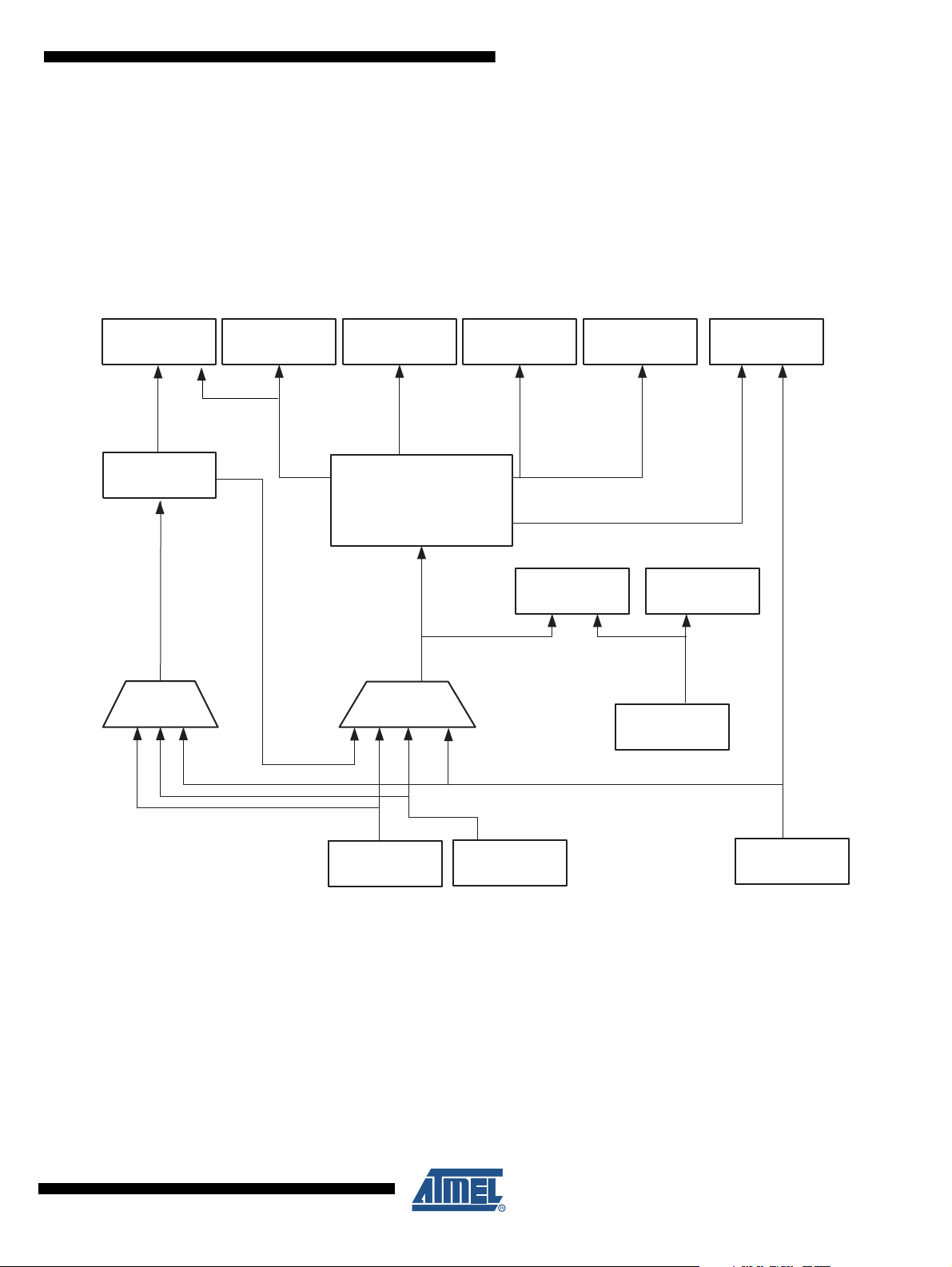
2.1 Block Diagram
The ATmega16/32/64/M1/C1 is a low-power CMOS 8-bit microcontroller based on the AVR
enhanced RISC architecture. By executing powerful instructions in a single clock cycle, the
ATmega16/32/64/M1/C1 achieves throughputs approaching 1 MIPS per MHz allowing the system designer to optimize power consumption versus processing speed.
Figure 2-1. Block Diagram
The AVR core combines a rich instruction set with 32 general purpose working registers. All the
32 registers are directly connected to the Arithmetic Logic Unit (ALU), allowing two independent
registers to be accessed in one single instruction executed in one clock cycle. The resulting
architecture is more code efficient while achieving throughputs up to ten times faster than conventional CISC microcontrollers.
8
Atmel ATmega16/32/64/M1/C1
7647H–AVR–03/12

Atmel ATmega16/32/64/M1/C1
The ATmega16/32/64/M1/C1 provides the following features: 16K/32K/64K bytes of In-System
Programmable Flash with Read-While-Write capabilities, 512/1024/2048 bytes EEPROM,
1024/2048/4096 bytes SRAM, 27 general purpose I/O lines, 32 general purpose working registers, one Motor Power Stage Controller, two flexible Timer/Counters with compare modes and
PWM, one UART with HW LIN, an 11-channel 10-bit ADC with two differential input stages with
programmable gain, a 10-bit DAC, a programmable Watchdog Timer with Internal Individual
Oscillator, an SPI serial port, an On-chip Debug system and four software selectable power saving modes.
The Idle mode stops the CPU while allowing the SRAM, Timer/Counters, SPI ports, CAN,
LIN/UART and interrupt system to continue functioning. The Power-down mode saves the register contents but freezes the Oscillator, disabling all other chip functions until the next interrupt or
Hardware Reset. The ADC Noise Reduction mode stops the CPU and all I/O modules except
ADC, to minimize switching noise during ADC conversions. In Standby mode, the Crystal/Resonator Oscillator is running while the rest of the device is sleeping. This allows very fast start-up
combined with low power consumption.
The device is manufactured using Atmel’s high-density nonvolatile memory technology. The
On-chip ISP Flash allows the program memory to be reprogrammed in-system through an SPI
serial interface, by a conventional nonvolatile memory programmer, or by an On-chip Boot program running on the AVR core. The boot program can use any interface to download the
application program in the application Flash memory. Software in the Boot Flash section will
continue to run while the Application Flash section is updated, providing true Read-While-Write
operation. By combining an 8-bit RISC CPU with In-System Self-Programmable Flash on a
monolithic chip, the Atmel ATmega16/32/64/M1/C1 is a powerful microcontroller that provides a
highly flexible and cost effective solution to many embedded control applications.
The ATmega16/32/64/M1/C1 AVR is supported with a full suite of program and system development tools including: C compilers, macro assemblers, program debugger/simulators, in-circuit
emulators, and evaluation kits.
2.2 Automotive Quality Grade
The ATmega16/32/64/M1/C1 have been developed and manufactured according to the most
stringent requirements of the international standard ISO-TS-16949. This data sheet contains
limit values extracted from the results of extensive characterization (Temperature and Voltage).
The quality and reliability of the ATmega16/32/64/M1/C1 have been verified during regular product qualification as per AEC-Q100 grade 1.
As indicated in the ordering information paragraph, the products are available in only one temperature grade.
Table 2-1. Temperature Grade Identification for Automotive Products
Temperature Temperature Identifier Comments
-40 ; +125 Z Full AutomotiveTemperature Range
7647H–AVR–03/12
9

2.3 Pin Descriptions
2.3.1 VCC
Digital supply voltage.
2.3.2 GND
Ground.
2.3.3 Port B (PB7..PB0)
Port B is an 8-bit bi-directional I/O port with internal pull-up resistors (selected for each bit). The
Port B output buffers have symmetrical drive characteristics with both high sink and source
capability. As inputs, Port B pins that are externally pulled low will source current if the pull-up
resistors are activated. The Port B pins are tri-stated when a reset condition becomes active,
even if the clock is not running.
Port B also serves the functions of various special features of the ATmega16/32/64/M1/C1 as
listed on page 69.
2.3.4 Port C (PC7..PC0)
Port C is an 8-bit bi-directional I/O port with internal pull-up resistors (selected for each bit). The
Port C output buffers have symmetrical drive characteristics with both high sink and source
capability. As inputs, Port C pins that are externally pulled low will source current if the pull-up
resistors are activated. The Port C pins are tri-stated when a reset condition becomes active,
even if the clock is not running.
Port C also serves the functions of special features of the ATmega16/32/64/M1/C1 as listed on
page 72.
2.3.5 Port D (PD7..PD0)
Port D is an 8-bit bi-directional I/O port with internal pull-up resistors (selected for each bit). The
Port D output buffers have symmetrical drive characteristics with both high sink and source
capability. As inputs, Port D pins that are externally pulled low will source current if the pull-up
resistors are activated. The Port D pins are tri-stated when a reset condition becomes active,
even if the clock is not running.
Port D also serves the functions of various special features of the ATmega16/32/64/M1/C1 as
listed on page 75.
2.3.6 Port E (PE2..0) RESET/
Port E is an 3-bit bi-directional I/O port with internal pull-up resistors (selected for each bit). The
Port E output buffers have symmetrical drive characteristics with both high sink and source
capability. As inputs, Port E pins that are externally pulled low will source current if the pull-up
resistors are activated. The Port E pins are tri-stated when a reset condition becomes active,
even if the clock is not running.
If the RSTDISBL Fuse is programmed, PE0 is used as an I/O pin. Note that the electrical characteristics of PE0 differ from those of the other pins of Port E.
If the RSTDISBL Fuse is unprogrammed, PE0 is used as a Reset input. A low level on this pin
for longer than the minimum pulse length will generate a Reset, even if the clock is not running.
The minimum pulse length is given in Table 7-1 on page 47. Shorter pulses are not guaranteed
to generate a Reset.
XTAL1/ XTAL2
10
Atmel ATmega16/32/64/M1/C1
7647H–AVR–03/12

Depending on the clock selection fuse settings, PE1 can be used as input to the inverting Oscillator amplifier and input to the internal clock operating circuit.
Depending on the clock selection fuse settings, PE2 can be used as output from the inverting
Oscillator amplifier.
The various special features of Port E are elaborated in “Alternate Functions of Port E” on page
78 and “Clock Systems and their Distribution” on page 29.
2.3.7 AVCC
AVCC is the supply voltage pin for the A/D Converter, D/A Converter, Current source. It should
be externally connected to V
be connected to V
Techniques” on page 238).
2.3.8 AREF
This is the analog reference pin for the A/D Converter.
2.4 About Code Examples
This documentation contains simple code examples that briefly show how to use various parts of
the device. These code examples assume that the part specific header file is included before
compilation. Be aware that not all C compiler vendors include bit definitions in the header files
and interrupt handling in C is compiler dependent. Please confirm with the C compiler documentation for more details.
Atmel ATmega16/32/64/M1/C1
, even if the ADC, DAC are not used. If the ADC is used, it should
CC
through a low-pass filter (see Section 18.6.2 “Analog Noise Canceling
CC
7647H–AVR–03/12
11
3. AVR CPU Core
Flash
Program
Memory
Instruction
Register
Instruction
Decoder
Program
Counter
Control Lines
32 x 8
General
Purpose
Registrers
ALU
Status
and Control
I/O Lines
EEPROM
Data Bus 8-bit
Data
SRAM
Direct Addressing
Indirect Addressing
Interrupt
Unit
SPI
Unit
Watchdog
Timer
Analog
Comparator
I/O Module 2
I/O Module1
I/O Module n
3.1 Introduction
This section discusses the AVR core architecture in general. The main function of the CPU core
is to ensure correct program execution. The CPU must therefore be able to access memories,
perform calculations, control peripherals, and handle interrupts.
3.2 Architectural Overview
Figure 3-1. Block Diagram of the AVR Architecture
In order to maximize performance and parallelism, the AVR uses a Harvard architecture – with
separate memories and buses for program and data. Instructions in the program memory are
executed with a single level pipelining. While one instruction is being executed, the next instruction is pre-fetched from the program memory. This concept enables instructions to be executed
in every clock cycle. The program memory is In-System Reprogrammable Flash memory.
12
Atmel ATmega16/32/64/M1/C1
7647H–AVR–03/12

Atmel ATmega16/32/64/M1/C1
The fast-access Register File contains 32 x 8-bit general purpose working registers with a single
clock cycle access time. This allows single-cycle Arithmetic Logic Unit (ALU) operation. In a typical ALU operation, two operands are output from the Register File, the operation is executed,
and the result is stored back in the Register File – in one clock cycle.
Six of the 32 registers can be used as three 16-bit indirect address register pointers for Data
Space addressing – enabling efficient address calculations. One of the these address pointers
can also be used as an address pointer for look up tables in Flash program memory. These
added function registers are the 16-bit X-, Y-, and Z-register, described later in this section.
The ALU supports arithmetic and logic operations between registers or between a constant and
a register. Single register operations can also be executed in the ALU. After an arithmetic operation, the Status Register is updated to reflect information about the result of the operation.
Program flow is provided by conditional and unconditional jump and call instructions, able to
directly address the whole address space. Most AVR instructions have a single 16-bit word format. Every program memory address contains a 16- or 32-bit instruction.
Program Flash memory space is divided in two sections, the Boot Program section and the
Application Program section. Both sections have dedicated Lock bits for write and read/write
protection. The SPM (Store Program Memory) instruction that writes into the Application Flash
memory section must reside in the Boot Program section.
During interrupts and subroutine calls, the return address Program Counter (PC) is stored on the
Stack. The Stack is effectively allocated in the general data SRAM, and consequently the Stack
size is only limited by the total SRAM size and the usage of the SRAM. All user programs must
initialize the SP in the Reset routine (before subroutines or interrupts are executed). The Stack
Pointer (SP) is read/write accessible in the I/O space. The data SRAM can easily be accessed
through the five different addressing modes supported in the AVR architecture.
The memory spaces in the AVR architecture are all linear and regular memory maps.
A flexible interrupt module has its control registers in the I/O space with an additional Global
Interrupt Enable bit in the Status Register. All interrupts have a separate Interrupt Vector in the
Interrupt Vector table. The interrupts have priority in accordance with their Interrupt Vector position. The lower the Interrupt Vector address, the higher is the priority.
The I/O memory space contains 64 addresses for CPU peripheral functions as Control Registers, SPI, and other I/O functions. The I/O Memory can be accessed directly, or as the Data
Space locations following those of the Register File, 0x20 - 0x5F. In addition, the
ATmega16/32/64/M1/C1 has Extended I/O space from 0x60 - 0xFF in SRAM where only the
ST/STS/STD and LD/LDS/LDD instructions can be used.
3.3 ALU – Arithmetic Logic Unit
The high-performance AVR ALU operates in direct connection with all the 32 general purpose
working registers. Within a single clock cycle, arithmetic operations between general purpose
registers or between a register and an immediate are executed. The ALU operations are divided
into three main categories – arithmetic, logical, and bit-functions. Some implementations of the
architecture also provide a powerful multiplier supporting both signed/unsigned multiplication
and fractional format. See the “Instruction Set” section for a detailed description.
7647H–AVR–03/12
13

3.4 Status Register
The Status Register contains information about the result of the most recently executed arithmetic instruction. This information can be used for altering program flow in order to perform
conditional operations. Note that the Status Register is updated after all ALU operations, as
specified in the Instruction Set Reference. This will in many cases remove the need for using the
dedicated compare instructions, resulting in faster and more compact code.
The Status Register is not automatically stored when entering an interrupt routine and restored
when returning from an interrupt. This must be handled by software.
The AVR Status Register – SREG – is defined as:
Bit 76543210
I T H S V N Z C SREG
Read/Write R/W R/W R/W R/W R/W R/W R/W R/W
Initial Value 0 0 0 0 0 0 0 0
• Bit 7 – I: Global Interrupt Enable
The Global Interrupt Enable bit must be set to enabled the interrupts. The individual interrupt
enable control is then performed in separate control registers. If the Global Interrupt Enable
Register is cleared, none of the interrupts are enabled independent of the individual interrupt
enable settings. The I-bit is cleared by hardware after an interrupt has occurred, and is set by
the RETI instruction to enable subsequent interrupts. The I-bit can also be set and cleared by
the application with the SEI and CLI instructions, as described in the instruction set reference.
• Bit 6 – T: Bit Copy Storage
The Bit Copy instructions BLD (Bit LoaD) and BST (Bit STore) use the T-bit as source or destination for the operated bit. A bit from a register in the Register File can be copied into T by the
BST instruction, and a bit in T can be copied into a bit in a register in the Register File by the
BLD instruction.
• Bit 5 – H: Half Carry Flag
The Half Carry Flag H indicates a Half Carry in some arithmetic operations. Half Carry Is useful
in BCD arithmetic. See the “Instruction Set Description” for detailed information.
• Bit 4 – S: Sign Bit, S = N
⊕ V
The S-bit is always an exclusive or between the negative flag N and the Two’s Complement
Overflow Flag V. See the “Instruction Set Description” for detailed information.
• Bit 3 – V: Two’s Complement Overflow Flag
The Two’s Complement Overflow Flag V supports two’s complement arithmetics. See the
“Instruction Set Description” for detailed information.
• Bit 2 – N: Negative Flag
The Negative Flag N indicates a negative result in an arithmetic or logic operation. See the
“Instruction Set Description” for detailed information.
• Bit 1 – Z: Zero Flag
The Zero Flag Z indicates a zero result in an arithmetic or logic operation. See the “Instruction
Set Description” for detailed information.
14
Atmel ATmega16/32/64/M1/C1
7647H–AVR–03/12

• Bit 0 – C: Carry Flag
The Carry Flag C indicates a carry in an arithmetic or logic operation. See the “Instruction Set
Description” for detailed information.
3.5 General Purpose Register File
The Register File is optimized for the AVR Enhanced RISC instruction set. In order to achieve
the required performance and flexibility, the following input/output schemes are supported by the
Register File:
• One 8-bit output operand and one 8-bit result input
• Two 8-bit output operands and one 8-bit result input
• Two 8-bit output operands and one 16-bit result input
• One 16-bit output operand and one 16-bit result input
Figure 3-2 shows the structure of the 32 general purpose working registers in the CPU.
Figure 3-2. AVR CPU General Purpose Working Registers
General R14 0x0E
Purpose R15 0x0F
Working R16 0x10
Registers R17 0x11
Atmel ATmega16/32/64/M1/C1
70Addr.
R0 0x00
R1 0x01
R2 0x02
…
R13 0x0D
…
R26 0x1A X-register Low Byte
R27 0x1B X-register High Byte
R28 0x1C Y-register Low Byte
R29 0x1D Y-register High Byte
R30 0x1E Z-register Low Byte
R31 0x1F Z-register High Byte
Most of the instructions operating on the Register File have direct access to all registers, and
most of them are single cycle instructions.
As shown in Figure 3-2, each register is also assigned a data memory address, mapping them
directly into the first 32 locations of the user Data Space. Although not being physically implemented as SRAM locations, this memory organization provides great flexibility in access of the
registers, as the X-, Y- and Z-pointer registers can be set to index any register in the file.
3.5.1 The X-register, Y-register, and Z-register
The registers R26..R31 have some added functions to their general purpose usage. These registers are 16-bit address pointers for indirect addressing of the data space. The three indirect
address registers X, Y, and Z are defined as described in Figure 3-3.
7647H–AVR–03/12
15
3.6 Stack Pointer
Figure 3-3. The X-, Y-, and Z-registers
15 XH XL 0
X-register 7 0 7 0
R27 (0x1B) R26 (0x1A)
15 YH YL 0
Y-register 7 0 7 0
R29 (0x1D) R28 (0x1C)
15 ZH ZL 0
Z-register 7 0 7 0
R31 (0x1F) R30 (0x1E)
In the different addressing modes these address registers have functions as fixed displacement,
automatic increment, and automatic decrement (see the instruction set reference for details).
The Stack is mainly used for storing temporary data, for storing local variables and for storing
return addresses after interrupts and subroutine calls. The Stack Pointer Register always points
to the top of the Stack. Note that the Stack is implemented as growing from higher memory locations to lower memory locations. This implies that a Stack PUSH command decreases the Stack
Pointer.
The Stack Pointer points to the data SRAM Stack area where the Subroutine and Interrupt
Stacks are located. This Stack space in the data SRAM must be defined by the program before
any subroutine calls are executed or interrupts are enabled. The Stack Pointer must be set to
point above 0x100. The Stack Pointer is decremented by one when data is pushed onto the
Stack with the PUSH instruction, and it is decremented by two when the return address is
pushed onto the Stack with subroutine call or interrupt. The Stack Pointer is incremented by one
when data is popped from the Stack with the POP instruction, and it is incremented by two when
data is popped from the Stack with return from subroutine RET or return from interrupt RETI.
The AVR Stack Pointer is implemented as two 8-bit registers in the I/O space. The number of
bits actually used is implementation dependent. Note that the data space in some implementations of the AVR architecture is so small that only SPL is needed. In this case, the SPH Register
will not be present.
Bit 1514131211109 8
SP15 SP14 SP13 SP12 SP11 SP10 SP9 SP8 SPH
SP7 SP6 SP5 SP4 SP3 SP2 SP1 SP0 SPL
76543210
Read/Write R/W R/W R/W R/W R/W R/W R/W R/W
R/W R/W R/W R/W R/W R/W R/W R/W
Initial Value Top address of the SRAM (0x04FF/0x08FF/0x10FF)
16
Atmel ATmega16/32/64/M1/C1
7647H–AVR–03/12
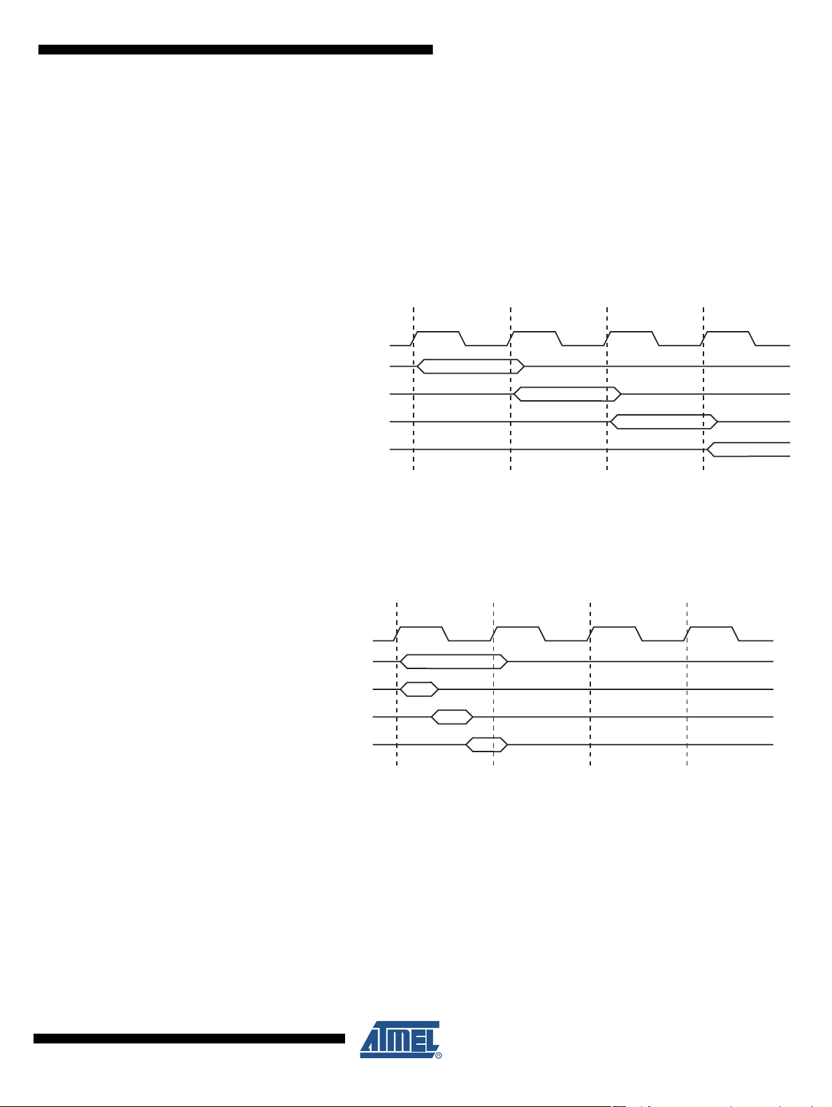
3.7 Instruction Execution Timing
clk
1st Instruction Fetch
1st Instruction Execute
2nd Instruction Fetch
2nd Instruction Execute
3rd Instruction Fetch
3rd Instruction Execute
4th Instruction Fetch
T1 T2 T3 T4
CPU
Total Execution Time
Register Operands Fetch
ALU Operation Execute
Result Write Back
T1 T2 T3 T4
clk
CPU
This section describes the general access timing concepts for instruction execution. The AVR
CPU is driven by the CPU clock clk
chip. No internal clock division is used.
Figure 3-4 shows the parallel instruction fetches and instruction executions enabled by the Har-
vard architecture and the fast-access Register File concept. This is the basic pipelining concept
to obtain up to 1 MIPS per MHz with the corresponding unique results for functions per cost,
functions per clocks, and functions per power-unit.
Figure 3-4. The Parallel Instruction Fetches and Instruction Executions
Atmel ATmega16/32/64/M1/C1
, directly generated from the selected clock source for the
CPU
Figure 3-5 shows the internal timing concept for the Register File. In a single clock cycle an ALU
operation using two register operands is executed, and the result is stored back to the destination register.
Figure 3-5. Single Cycle ALU Operation
3.8 Reset and Interrupt Handling
The AVR provides several different interrupt sources. These interrupts and the separate Reset
Vector each have a separate program vector in the program memory space. All interrupts are
assigned individual enable bits which must be written logic one together with the Global Interrupt
Enable bit in the Status Register in order to enable the interrupt. Depending on the Program
Counter value, interrupts may be automatically disabled when Boot Lock bits BLB02 or BLB12
are programmed. This feature improves software security. See the section “Memory Program-
ming” on page 296 for details.
7647H–AVR–03/12
17

The lowest addresses in the program memory space are by default defined as the Reset and
Interrupt Vectors. The complete list of vectors is shown in “Interrupts” on page 57. The list also
determines the priority levels of the different interrupts. The lower the address the higher is the
priority level. RESET has the highest priority, and next is ANACOMP0 – the Analog Comparator
0 Interrupt. The Interrupt Vectors can be moved to the start of the Boot Flash section by setting
the IVSEL bit in the MCU Control Register (MCUCR). Refer to “Interrupts” on page 57 for more
information. The Reset Vector can also be moved to the start of the Boot Flash section by programming the BOOTRST Fuse, see “Boot Loader Support – Read-While-Write
Self-Programming ATmega16/32/64/M1/C1” on page 279.
3.8.1 Interrupt Behavior
When an interrupt occurs, the Global Interrupt Enable I-bit is cleared and all interrupts are disabled. The user software can write logic one to the I-bit to enable nested interrupts. All enabled
interrupts can then interrupt the current interrupt routine. The I-bit is automatically set when a
Return from Interrupt instruction – RETI – is executed.
There are basically two types of interrupts. The first type is triggered by an event that sets the
interrupt flag. For these interrupts, the Program Counter is vectored to the actual Interrupt Vector
in order to execute the interrupt handling routine, and hardware clears the corresponding interrupt flag. Interrupt flags can also be cleared by writing a logic one to the flag bit position(s) to be
cleared. If an interrupt condition occurs while the corresponding interrupt enable bit is cleared,
the interrupt flag will be set and remembered until the interrupt is enabled, or the flag is cleared
by software. Similarly, if one or more interrupt conditions occur while the Global Interrupt Enable
bit is cleared, the corresponding interrupt flag(s) will be set and remembered until the Global
Interrupt Enable bit is set, and will then be executed by order of priority.
The second type of interrupts will trigger as long as the interrupt condition is present. These
interrupts do not necessarily have interrupt flags. If the interrupt condition disappears before the
interrupt is enabled, the interrupt will not be triggered.
When the AVR exits from an interrupt, it will always return to the main program and execute one
more instruction before any pending interrupt is served.
Note that the Status Register is not automatically stored when entering an interrupt routine, nor
restored when returning from an interrupt routine. This must be handled by software.
When using the CLI instruction to disable interrupts, the interrupts will be immediately disabled.
No interrupt will be executed after the CLI instruction, even if it occurs simultaneously with the
CLI instruction. The following example shows how this can be used to avoid interrupts during the
timed EEPROM write sequence.
18
Atmel ATmega16/32/64/M1/C1
7647H–AVR–03/12

Atmel ATmega16/32/64/M1/C1
Assembly Code Example
in r16, SREG ; store SREG value
cli ; disable interrupts during timed sequence
sbi EECR, EEMWE ; start EEPROM write
sbi EECR, EEWE
out SREG, r16 ; restore SREG value (I-bit)
C Code Example
char cSREG;
cSREG = SREG; /* store SREG value */
/* disable interrupts during timed sequence */
_CLI();
EECR |= (1<<EEMWE); /* start EEPROM write */
EECR |= (1<<EEWE);
SREG = cSREG; /* restore SREG value (I-bit) */
When using the SEI instruction to enable interrupts, the instruction following SEI will be executed before any pending interrupts, as shown in this example.
Assembly Code Example
C Code Example
3.8.2 Interrupt Response Time
The interrupt execution response for all the enabled AVR interrupts is four clock cycles minimum. After four clock cycles the program vector address for the actual interrupt handling routine
is executed. During this four clock cycle period, the Program Counter is pushed onto the Stack.
The vector is normally a jump to the interrupt routine, and this jump takes three clock cycles. If
an interrupt occurs during execution of a multi-cycle instruction, this instruction is completed
before the interrupt is served. If an interrupt occurs when the MCU is in sleep mode, the interrupt
execution response time is increased by four clock cycles. This increase comes in addition to the
start-up time from the selected sleep mode.
A return from an interrupt handling routine takes four clock cycles. During these four clock
cycles, the Program Counter (two bytes) is popped back from the Stack, the Stack Pointer is
incremented by two, and the I-bit in SREG is set.
sei ; set Global Interrupt Enable
sleep; enter sleep, waiting for interrupt
; note: will enter sleep before any pending
; interrupt(s)
_SEI(); /* set Global Interrupt Enable */
_SLEEP(); /* enter sleep, waiting for interrupt */
/* note: will enter sleep before any pending interrupt(s) */
7647H–AVR–03/12
19

4. Memories
F
This section describes the different memories in the ATmega16/32/64/M1/C1. The AVR architecture has two main memory spaces, the Data Memory and the Program Memory space. In
addition, the ATmega16/32/64/M1/C1 features an EEPROM Memory for data storage. All three
memory spaces are linear and regular.
4.1 In-System Reprogrammable Flash Program Memory
The ATmega16/32/64/M1/C1 contains 16K/32K/64K bytes On-chip In-System Reprogrammable
Flash memory for program storage. Since all AVR instructions are 16 or 32 bits wide, the Flash
is organized as 8K x 16, 16K x 16 , 32K x 16. For software security, the Flash Program memory
space is divided into two sections, Boot Program section and Application Program section.
The Flash memory has an endurance of at least 10,000 write/erase cycles. The
ATmega16/32/64/M1/C1 Program Counter (PC) is 14/15 bits wide, thus addressing the
8K/16K/32K program memory locations. The operation of Boot Program section and associated
Boot Lock bits for software protection are described in detail in “Boot Loader Support –
Read-While-Write Self-Programming ATmega16/32/64/M1/C1” on page 279. “Memory Programming” on page 296 contains a detailed description on Flash programming in SPI or Parallel
programming mode.
Constant tables can be allocated within the entire program memory address space (see the LPM
– Load Program Memory.
Timing diagrams for instruction fetch and execution are presented in “Instruction Execution Tim-
ing” on page 17.
Figure 4-1. Program Memory Map
Program Memory
Application Flash Section
Boot Flash Section
0x0000
0x1FFF/0x3FFF/0x7
20
Atmel ATmega16/32/64/M1/C1
7647H–AVR–03/12

4.2 SRAM Data Memory
Figure 4-2 shows how the ATmega16/32/64/M1/C1 SRAM Memory is organized.
The ATmega16/32/64/M1/C1 is a complex microcontroller with more peripheral units than can
be supported within the 64 locations reserved in the Opcode for the IN and OUT instructions. For
the Extended I/O space from 0x60 - 0xFF in SRAM, only the ST/STS/STD and LD/LDS/LDD
instructions can be used.
The lower 2304 data memory locations address both the Register File, the I/O memory,
Extended I/O memory, and the internal data SRAM. The first 32 locations address the Register
File, the next 64 location the standard I/O memory, then 160 locations of Extended I/O memory,
and the next 1024/2048/4096 locations address the internal data SRAM.
The five different addressing modes for the data memory cover: Direct, Indirect with Displacement, Indirect, Indirect with Pre-decrement, and Indirect with Post-increment. In the Register
File, registers R26 to R31 feature the indirect addressing pointer registers.
The direct addressing reaches the entire data space.
The Indirect with Displacement mode reaches 63 address locations from the base address given
by the Y- or Z-register.
When using register indirect addressing modes with automatic pre-decrement and post-incre-
ment, the address registers X, Y, and Z are decremented or incremented.
Atmel ATmega16/32/64/M1/C1
The 32 general purpose working registers, 64 I/O Registers, 160 Extended I/O Registers, and
the 1024/2048/4096 bytes of internal data SRAM in the ATmega16/32/64/M1/C1 are all accessible through all these addressing modes. The Register File is described in “General Purpose
Register File” on page 15.
Figure 4-2. Data Memory Map for 1024/2048/4096 Internal SRAM
4.2.1 SRAM Data Access Times
This section describes the general access timing concepts for internal memory access.
The internal data SRAM access is performed in two clk
page 22.
Data Memory
32 Registers
64 I/O Registers
160 Ext I/O Reg.
Internal SRAM
(1024x8)
(2048x8)
(4096x8)
0x0000 - 0x001F
0x0020 - 0x005F
0x0060 - 0x00FF
0x0100
0x04FF/0x08FF/0x10FF
cycles as described in Figure 4-3 on
CPU
7647H–AVR–03/12
21
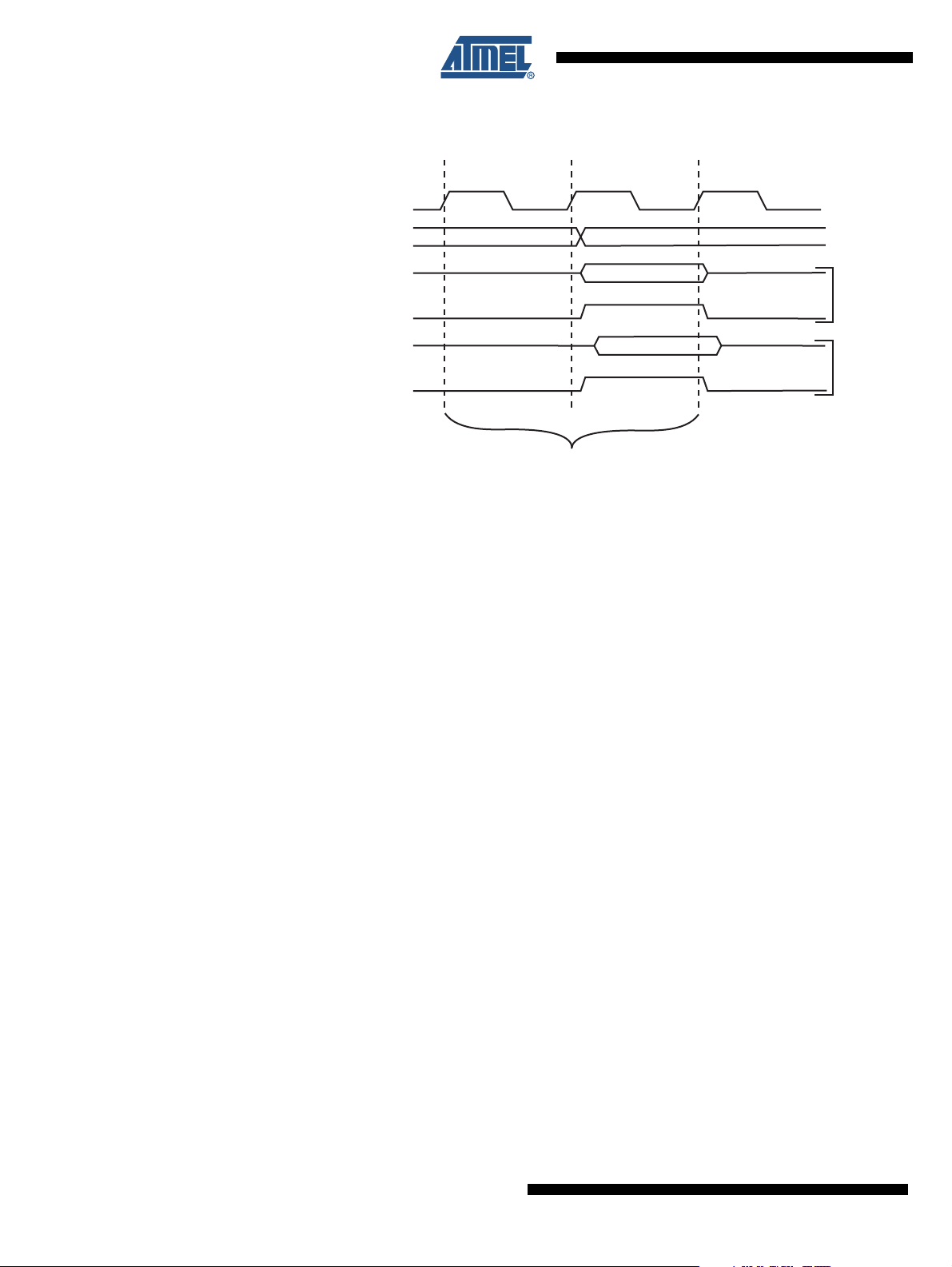
Figure 4-3. On-chip Data SRAM Access Cycles
clk
WR
RD
Data
Data
Address
Address valid
T1 T2 T3
Compute Address
Read
Write
CPU
Memory Access Instruction
Next Instruction
4.3 EEPROM Data Memory
The ATmega16/32/64/M1/C1 contains 512/1024/2048 bytes of data EEPROM memory. It is
organized as a separate data space, in which single bytes can be read and written. The
EEPROM has an endurance of at least 100,000 write/erase cycles. The access between the
EEPROM and the CPU is described in the following, specifying the EEPROM Address Registers, the EEPROM Data Register, and the EEPROM Control Register.
For a detailed description of SPI and Parallel data downloading to the EEPROM, see “Serial
Downloading” on page 313 , and “Parallel Programming Parameters, Pin Mapping, and Commands” on page 301 respectively.
4.3.1 EEPROM Read/Write Access
The EEPROM Access Registers are accessible in the I/O space.
The write access time for the EEPROM is given in Table 4-2. A self-timing function, however,
lets the user software detect when the next byte can be written. If the user code contains instructions that write the EEPROM, some precautions must be taken. In heavily filtered power
supplies, V
period of time to run at a voltage lower than specified as minimum for the clock frequency used.
See “Preventing EEPROM Corruption” on page 27.for details on how to avoid problems in these
situations.
In order to prevent unintentional EEPROM writes, a specific write procedure must be followed.
Refer to the description of the EEPROM Control Register for details on this.
When the EEPROM is read, the CPU is halted for four clock cycles before the next instruction is
executed. When the EEPROM is written, the CPU is halted for two clock cycles before the next
instruction is executed.
CC
is likely to rise or fall slowly on power-up/down. This causes the device for some
22
Atmel ATmega16/32/64/M1/C1
7647H–AVR–03/12
Atmel ATmega16/32/64/M1/C1
4.3.2 The EEPROM Address Registers – EEARH and EEARL
Bit 15141312 11 10 9 8
– – – – – EEAR10 EEAR9 EEAR8 EEARH
EEAR7 EEAR6 EEAR5 EEAR4 EEAR3 EEAR2 EEAR1 EEAR0 EEARL
76543 2 10
Read/Write R R R R R R/W R/W R/W
R/W R/W R/W R/W R/W R/W R/W R/W
Initial Value 0 0 0 0 0 X X X
XXXX X X XX
• Bits 15.11 – Reserved Bits
These bits are reserved bits in the ATmega16/32/64/M1/C1 and will always read as zero.
• Bits 9..0 – EEAR10..0: EEPROM Address
The EEPROM Address Registers – EEARH and EEARL specify the EEPROM address in the
512/1024/2048 bytes EEPROM space. The EEPROM data bytes are addressed linearly
between 0 and 511/1023/2047. The initial value of EEAR is undefined. A proper value must be
written before the EEPROM may be accessed.
4.3.3 The EEPROM Data Register – EEDR
Bit 76543210
EEDR7 EEDR6 EEDR5 EEDR4 EEDR3 EEDR2 EEDR1 EEDR0 EEDR
Read/Write R/W R/W R/W R/W R/W R/W R/W R/W
Initial Value00000000
• Bits 7..0 – EEDR7.0: EEPROM Data
For the EEPROM write operation, the EEDR Register contains the data to be written to the
EEPROM in the address given by the EEAR Register. For the EEPROM read operation, the
EEDR contains the data read out from the EEPROM at the address given by EEAR.
4.3.4 The EEPROM Control Register – EECR
Bit 76543210
– – EEPM1 EEPM0 EERIE EEMWE EEWE EERE EECR
Read/Write R R R/W R/W R/W R/W R/W R/W
Initial Value 0 0 X X 0 0 X 0
• Bits 7..6 – Reserved Bits
These bits are reserved bits in the ATmega16/32/64/M1/C1 and will always read as zero.
• Bits 5..4 – EEPM1 and EEPM0: EEPROM Programming Mode Bits
The EEPROM Programming mode bit setting defines which programming action that will be triggered when writing EEWE. It is possible to program data in one atomic operation (erase the old
value and program the new value) or to split the Erase and Write operations in two different
operations. The Programming times for the different modes are shown in Table 4-1 on page 24.
7647H–AVR–03/12
23

While EEWE is set, any write to EEPMn will be ignored. During reset, the EEPMn bits will be
reset to 0b00 unless the EEPROM is busy programming.
Table 4-1. EEPROM Mode Bits
EEPM1 EEPM0 Programming Time Operation
0 0 3.4 ms Erase and Write in one operation (Atomic Operation)
0 1 1.8 ms Erase Only
1 0 1.8 ms Write Only
1 1 – Reserved for future use
• Bit 3 – EERIE: EEPROM Ready Interrupt Enable
Writing EERIE to one enables the EEPROM Ready Interrupt if the I bit in SREG is set. Writing
EERIE to zero disables the interrupt. The EEPROM Ready interrupt generates a constant interrupt when EEWE is cleared. The interrupt will not be generated during EEPROM write or SPM.
• Bit 2 – EEMWE: EEPROM Master Write Enable
The EEMWE bit determines whether setting EEWE to one causes the EEPROM to be written.
When EEMWE is set, setting EEWE within four clock cycles will write data to the EEPROM at
the selected address If EEMWE is zero, setting EEWE will have no effect. When EEMWE has
been written to one by software, hardware clears the bit to zero after four clock cycles. See the
description of the EEWE bit for an EEPROM write procedure.
• Bit 1 – EEWE: EEPROM Write Enable
The EEPROM Write Enable Signal EEWE is the write strobe to the EEPROM. When address
and data are correctly set up, the EEWE bit must be written to one to write the value into the
EEPROM. The EEMWE bit must be written to one before a logical one is written to EEWE, otherwise no EEPROM write takes place. The following procedure should be followed when writing
the EEPROM (the order of steps 3 and 4 is not essential):
1. Wait until EEWE becomes zero.
2. Wait until SPMEN (Store Program Memory Enable) in SPMCSR (Store Program Memory
Control and Status Register) becomes zero.
3. Write new EEPROM address to EEAR (optional).
4. Write new EEPROM data to EEDR (optional).
5. Write a logical one to the EEMWE bit while writing a zero to EEWE in EECR.
6. Within four clock cycles after setting EEMWE, write a logical one to EEWE.
The EEPROM can not be programmed during a CPU write to the Flash memory. The software
must check that the Flash programming is completed before initiating a new EEPROM write.
Step 2 is only relevant if the software contains a Boot Loader allowing the CPU to program the
Flash. If the Flash is never being updated by the CPU, step 2 can be omitted. See “Boot Loader
Support – Read-While-Write Self-Programming ATmega16/32/64/M1/C1” on page 279 for
details about Boot programming.
Caution: An interrupt between step 5 and step 6 will make the write cycle fail, since the
EEPROM Master Write Enable will time-out. If an interrupt routine accessing the EEPROM is
interrupting another EEPROM access, the EEAR or EEDR Register will be modified, causing the
interrupted EEPROM access to fail. It is recommended to have the Global Interrupt Flag cleared
during all the steps to avoid these problems.
24
When the write access time has elapsed, the EEWE bit is cleared by hardware. The user software can poll this bit and wait for a zero before writing the next byte. When EEWE has been set,
the CPU is halted for two cycles before the next instruction is executed.
Atmel ATmega16/32/64/M1/C1
7647H–AVR–03/12

Atmel ATmega16/32/64/M1/C1
• Bit 0 – EERE: EEPROM Read Enable
The EEPROM Read Enable Signal EERE is the read strobe to the EEPROM. When the correct
address is set up in the EEAR Register, the EERE bit must be written to a logic one to trigger the
EEPROM read. The EEPROM read access takes one instruction, and the requested data is
available immediately. When the EEPROM is read, the CPU is halted for four cycles before the
next instruction is executed.
The user should poll the EEWE bit before starting the read operation. If a write operation is in
progress, it is neither possible to read the EEPROM, nor to change the EEAR Register.
The calibrated Oscillator is used to time the EEPROM accesses. Table 4-2 lists the typical programming time for EEPROM access from the CPU.
Table 4-2. EEPROM Programming Time.
Symbol Number of Calibrated RC Oscillator Cycles Typ Programming Time
EEPROM write
(from CPU)
The following code examples show one assembly and one C function for writing to the
EEPROM. The examples assume that interrupts are controlled (e.g. by disabling interrupts globally) so that no interrupts will occur during execution of these functions. The examples also
assume that no Flash Boot Loader is present in the software. If such code is present, the
EEPROM write function must also wait for any ongoing SPM command to finish.
26368 3.3 ms
7647H–AVR–03/12
25

Assembly Code Example
EEPROM_write:
; Wait for completion of previous write
sbic EECR,EEWE
rjmp EEPROM_write
; Set up address (r18:r17) in address register
out EEARH, r18
out EEARL, r17
; Write data (r16) to data register
out EEDR,r16
; Write logical one to EEMWE
sbi EECR,EEMWE
; Start eeprom write by setting EEWE
sbi EECR,EEWE
ret
C Code Example
void EEPROM_write (unsigned int uiAddress, unsigned char ucData)
{
/* Wait for completion of previous write */
while(EECR & (1<<EEWE))
;
/* Set up address and data registers */
EEAR = uiAddress;
EEDR = ucData;
/* Write logical one to EEMWE */
EECR |= (1<<EEMWE);
/* Start eeprom write by setting EEWE */
EECR |= (1<<EEWE);
}
26
Atmel ATmega16/32/64/M1/C1
7647H–AVR–03/12

Atmel ATmega16/32/64/M1/C1
The next code examples show assembly and C functions for reading the EEPROM. The examples assume that interrupts are controlled so that no interrupts will occur during execution of
these functions.
Assembly Code Example
EEPROM_read:
; Wait for completion of previous write
sbic EECR,EEWE
rjmp EEPROM_read
; Set up address (r18:r17) in address register
out EEARH, r18
out EEARL, r17
; Start eeprom read by writing EERE
sbi EECR,EERE
; Read data from data register
in r16,EEDR
ret
C Code Example
unsigned char EEPROM_read(unsigned int uiAddress)
{
/* Wait for completion of previous write */
while(EECR & (1<<EEWE))
;
/* Set up address register */
EEAR = uiAddress;
/* Start eeprom read by writing EERE */
EECR |= (1<<EERE);
/* Return data from data register */
return EEDR;
}
4.3.5 Preventing EEPROM Corruption
During periods of low V
too low for the CPU and the EEPROM to operate properly. These issues are the same as for
board level systems using EEPROM, and the same design solutions should be applied.
An EEPROM data corruption can be caused by two situations when the voltage is too low. First,
a regular write sequence to the EEPROM requires a minimum voltage to operate correctly. Secondly, the CPU itself can execute instructions incorrectly, if the supply voltage is too low.
EEPROM data corruption can easily be avoided by following this design recommendation:
the EEPROM data can be corrupted because the supply voltage is
CC,
7647H–AVR–03/12
Keep the AVR RESET active (low) during periods of insufficient power supply voltage. This can
be done by enabling the internal Brown-out Detector (BOD). If the detection level of the internal
BOD does not match the needed detection level, an external low V
reset Protection circuit can
CC
be used. If a reset occurs while a write operation is in progress, the write operation will be completed provided that the power supply voltage is sufficient.
27
4.4 I/O Memory
The I/O space definition of the ATmega16/32/64/M1/C1 is shown in “Register Summary” on
page 347.
All ATmega16/32/64/M1/C1 I/Os and peripherals are placed in the I/O space. All I/O locations
may be accessed by the LD/LDS/LDD and ST/STS/STD instructions, transferring data between
the 32 general purpose working registers and the I/O space. I/O registers within the address
range 0x00 - 0x1F are directly bit-accessible using the SBI and CBI instructions. In these registers, the value of single bits can be checked by using the SBIS and SBIC instructions. Refer to
the instruction set section for more details. When using the I/O specific commands IN and OUT,
the I/O addresses 0x00 - 0x3F must be used. When addressing I/O registers as data space
using LD and ST instructions, 0x20 must be added to these addresses. The
ATmega16/32/64/M1/C1 is a complex microcontroller with more peripheral units than can be
supported within the 64 location reserved in Opcode for the IN and OUT instructions. For the
Extended I/O space from 0x60 - 0xFF in SRAM, only the ST/STS/STD and LD/LDS/LDD instructions can be used.
For compatibility with future devices, reserved bits should be written to zero if accessed.
Reserved I/O memory addresses should never be written.
Some of the status flags are cleared by writing a logical one to them. Note that, unlike most other
AVR’s, the CBI and SBI instructions will only operate on the specified bit, and can therefore be
used on registers containing such status flags. The CBI and SBI instructions work with registers
0x00 to 0x1F only.
The I/O and peripherals control registers are explained in later sections.
4.5 General Purpose I/O Registers
The ATmega16/32/64/M1/C1 contains four General Purpose I/O Registers. These registers can
be used for storing any information, and they are particularly useful for storing global variables
and status flags.
The General Purpose I/O Registers, within the address range 0x00 - 0x1F, are directly
bit-accessible using the SBI, CBI, SBIS, and SBIC instructions.
4.5.1 General Purpose I/O Register 0 – GPIOR0
Bit 76543210
GPIOR07 GPIOR06 GPIOR05 GPIOR04 GPIOR03 GPIOR02 GPIOR01 GPIOR00 GPIOR0
Read/Write R/W R/W R/W R/W R/W R/W R/W R/W
Initial Value00000000
4.5.2 General Purpose I/O Register 1 – GPIOR1
Bit 76543210
GPIOR17 GPIOR16 GPIOR15 GPIOR14 GPIOR13 GPIOR12 GPIOR11 GPIOR10 GPIOR1
Read/Write R/W R/W R/W R/W R/W R/W R/W R/W
Initial Value00000000
4.5.3 General Purpose I/O Register 2 – GPIOR2
Bit 76543210
GPIOR27 GPIOR26 GPIOR25 GPIOR24 GPIOR23 GPIOR22 GPIOR21 GPIOR20 GPIOR2
Read/Write R/W R/W R/W R/W R/W R/W R/W R/W
Initial Value00000000
28
Atmel ATmega16/32/64/M1/C1
7647H–AVR–03/12
5. System Clock
General I/O
Modules
ADC CPU Core RAM
clk
I/O
AVR Clock
Control Unit
clk
CPU
Flash and
EEPROM
clk
FLASH
clk
ADC
Source Clock
Watchdog Timer
Watchdog
Oscillator
Reset Logic
Clock
Multiplexer
Watchdog Clock
Calibrated RC
Oscillator
(Crystal
Oscillator)
External Clock
Fast Peripherals
PLL
CLK
PLL
Multiplexer
PLL Input
5.1 Clock Systems and their Distribution
Figure 5-1 presents the principal clock systems in the AVR and their distribution. All of the clocks
need not be active at a given time. In order to reduce power consumption, the clocks to unused
modules can be halted by using different sleep modes, as described in “Power Management and
Sleep Modes” on page 40. The clock systems are detailed below.
Figure 5-1. Clock Distribution
Atmel ATmega16/32/64/M1/C1
5.1.1 CPU Clock – clk
5.1.2 I/O Clock – clk
CPU
The CPU clock is routed to parts of the system concerned with operation of the AVR core.
Examples of such modules are the General Purpose Register File, the Status Register and the
data memory holding the Stack Pointer. Halting the CPU clock inhibits the core from performing
general operations and calculations.
I/O
The I/O clock is used by the majority of the I/O modules, like Timer/Counters, SPI, UART. The
I/O clock is also used by the External Interrupt module, but note that some external interrupts
are detected by asynchronous logic, allowing such interrupts to be detected even if the I/O clock
is halted.
7647H–AVR–03/12
29

5.1.3 Flash Clock – clk
The Flash clock controls operation of the Flash interface. The Flash clock is usually active simultaneously with the CPU clock.
FLASH
5.1.4 PLL Clock – clk
5.1.5 ADC Clock – clk
5.2 Clock Sources
PLL
The PLL clock allows the fast peripherals to be clocked directly from a 64/32MHz clock. A
16MHz clock is also derived for the CPU.
ADC
The ADC is provided with a dedicated clock domain. This allows halting the CPU and I/O clocks
in order to reduce noise generated by digital circuitry. This gives more accurate ADC conversion
results.
The device has the following clock source options, selectable by Flash Fuse bits as illustrated
Table 5-1. The clock from the selected source is input to the AVR clock generator, and routed to
the appropriate modules.
Table 5-1. Device Clocking Options Select
Device Clocking Option
External Crystal/Ceramic Resonator Ext Osc RC Osc 1111 - 1000
PLL output divided by 4 : 16MHz / PLL driven by External
Crystal/Ceramic Resonator
(1)
System
Clock PLL Input CKSEL3..0
Ext Osc Ext Osc 0100
PLL output divided by 4 : 16MHz / PLL driven by External
Crystal/Ceramic Resonator
Reserved N/A N/A 0110
Reserved N/A N/A 0111
PLL output divided by 4 : 16MHz PLL / 4 RC Osc 0011
Calibrated Internal RC Oscillator RC Osc RC Osc 0010
PLL output divided by 4 : 16MHz / PLL driven by External
clock
External Clock Ext Clk RC Osc 0000
Note: 1. For all fuses “1” means unprogrammed while “0” means programmed.
2. Ext Osc : External Osc
3. RC Osc : Internal RC Oscillator
4. Ext Clk : External Clock Input
PLL / 4 Ext Osc 0101
PLL / 4 Ext Clk 0001
The various choices for each clocking option is given in the following sections. When the CPU
wakes up from Power-down or Power-save, the selected clock source is used to time the
start-up, ensuring stable Oscillator operation before instruction execution starts. When the CPU
starts from reset, there is an additional delay allowing the power to reach a stable level before
starting normal operation. The Watchdog Oscillator is used for timing this real-time part of the
start-up time. The number of WDT Oscillator cycles used for each time-out is shown in Table
5-2. The frequency of the Watchdog Oscillator is voltage dependent as shown in “Watchdog
Oscillator Frequency versus V
” on page 342.
CC
30
Atmel ATmega16/32/64/M1/C1
7647H–AVR–03/12
 Loading...