

Artesyn MVME55006E Installation

MVME55006E Single Board Computer
Installation and Use
P/N: 6806800A37J
July 2014

©
Copyright 2014 Artesyn Embedded Technologies, Inc.
All rights reserved.
Trademarks
Artesyn Embedded Technologies, Artesyn and the Artesyn Embedded Technologies logo are trademarks and service marks of
Artesyn Embedded Technologies, Inc.© 2014 Artesyn Embedded Technologies, Inc. All other product or service names are the
property of their respective owners.
Intel® is a trademark or registered trademark of Intel Corporation or its subsidiaries in the United States and other countries.
Java™ and all other Java-based marks are trademarks or registered trademarks of Oracle America, Inc. in the U.S. and other countries.
Microsoft®, Windows® and Windows Me® are registered trademarks of Microsoft Corporation; and Windows XP™ is a trademark of
Microsoft Corporation.
PICMG®, CompactPCI®, AdvancedTCA™ and the PICMG, CompactPCI and AdvancedTCA logos are registered trademarks of the PCI
Industrial Computer Manufacturers Group.
UNIX® is a registered trademark of The Open Group in the United States and other countries.
Notice
While reasonable efforts have been made to assure the accuracy of this document, Artesyn assumes no liability resulting from any
omissions in this document, or from the use of the information obtained therein. Artesyn reserves the right to revise this document
and to make changes from time to time in the content hereof without obligation of Artesyn to notify any person of such revision or
changes.
Electronic versions of this material may be read online, downloaded for personal use, or referenced in another document as a URL to
an Artesyn website. The text itself may not be published commercially in print or electronic form, edited, translated, or otherwise
altered without the permission of Artesyn.
It is possible that this publication may contain reference to or information about Artesyn products (machines and programs),
programming, or services that are not available in your country. Such references or information must not be construed to mean that
Artesyn intends to announce such Artesyn products, programming, or services in your country.
Limited and Restricted Rights Legend
If the documentation contained herein is supplied, directly or indirectly, to the U.S. Government, the following notice shall apply
unless otherwise agreed to in writing by Artesyn.
Use, duplication, or disclosure by the Government is subject to restrictions as set forth in subparagraph (b)(3) of the Rights in
Technical Data clause at DFARS 252.227-7013 (Nov. 1995) and of the Rights in Noncommercial Computer Software and
Documentation clause at DFARS 252.227-7014 (Jun. 1995).
Contact Address
Artesyn Embedded Technologies Artesyn Embedded Technologies
Marketing Communications
2900 S. Diablo Way, Suite 190
Tempe, Arizona 85282
Lilienthalstr. 17-19
85579 Neubiberg/Munich
Germany

Contents
Contents
About this Manual . . . . . . . . . . . . . . . . . . . . . . . . . . . . . . . . . . . . . . . . . . . . . . . . . . . . . . . . . . . . . . . . . . . . . . . 13
1 Hardware Preparation and Installation . . . . . . . . . . . . . . . . . . . . . . . . . . . . . . . . . . . . . . . . . . . . . . . . . 19
1.1 Overview . . . . . . . . . . . . . . . . . . . . . . . . . . . . . . . . . . . . . . . . . . . . . . . . . . . . . . . . . . . . . . . . . . . . . . . . . . 19
1.2 Introduction . . . . . . . . . . . . . . . . . . . . . . . . . . . . . . . . . . . . . . . . . . . . . . . . . . . . . . . . . . . . . . . . . . . . . . . 19
1.3 Declaration of Conformity . . . . . . . . . . . . . . . . . . . . . . . . . . . . . . . . . . . . . . . . . . . . . . . . . . . . . . . . . . . 20
1.4 Getting Started . . . . . . . . . . . . . . . . . . . . . . . . . . . . . . . . . . . . . . . . . . . . . . . . . . . . . . . . . . . . . . . . . . . . 21
1.5 Overview of Startup Procedures . . . . . . . . . . . . . . . . . . . . . . . . . . . . . . . . . . . . . . . . . . . . . . . . . . . . . . 21
1.6 Unpacking Guidelines . . . . . . . . . . . . . . . . . . . . . . . . . . . . . . . . . . . . . . . . . . . . . . . . . . . . . . . . . . . . . . . 21
1.7 Configuring the Hardware . . . . . . . . . . . . . . . . . . . . . . . . . . . . . . . . . . . . . . . . . . . . . . . . . . . . . . . . . . . 22
1.7.1 Configuring the Board . . . . . . . . . . . . . . . . . . . . . . . . . . . . . . . . . . . . . . . . . . . . . . . . . . . . . . . . 23
1.7.2 Ethernet 2, PMC/SBC Mode, and P2 I/O Selection Headers (J6, J7, J28, J32, J34, J97 – J110)
26
1.7.2.1 Ethernet . . . . . . . . . . . . . . . . . . . . . . . . . . . . . . . . . . . . . . . . . . . . . . . . . . . . . . . . . . . 27
1.7.2.2 PMC/SBC Mode Selection . . . . . . . . . . . . . . . . . . . . . . . . . . . . . . . . . . . . . . . . . . . . 27
1.7.2.3 P2 I/O Selection . . . . . . . . . . . . . . . . . . . . . . . . . . . . . . . . . . . . . . . . . . . . . . . . . . . . . 28
1.7.3 Flash Boot Bank Select Header (J8) . . . . . . . . . . . . . . . . . . . . . . . . . . . . . . . . . . . . . . . . . . . . . 30
1.7.4 Flash 0 Programming Enable Switch (S3-1) . . . . . . . . . . . . . . . . . . . . . . . . . . . . . . . . . . . . . . 31
1.7.5 Safe Start ENV Switch (S5-1). . . . . . . . . . . . . . . . . . . . . . . . . . . . . . . . . . . . . . . . . . . . . . . . . . . 31
1.7.6 Flash 0 Block Write Protect Switch (S3-2). . . . . . . . . . . . . . . . . . . . . . . . . . . . . . . . . . . . . . . . 32
1.7.7 SROM Initialization Enable Switch (S5-2) . . . . . . . . . . . . . . . . . . . . . . . . . . . . . . . . . . . . . . . . 32
1.7.8 PCI Bus 0.0 Speed Switch (S4-1). . . . . . . . . . . . . . . . . . . . . . . . . . . . . . . . . . . . . . . . . . . . . . . . 33
1.7.9 VME SCON Select Header (J27). . . . . . . . . . . . . . . . . . . . . . . . . . . . . . . . . . . . . . . . . . . . . . . . . 33
1.7.10 PCI Bus 1.0 Speed Switch (S4-2). . . . . . . . . . . . . . . . . . . . . . . . . . . . . . . . . . . . . . . . . . . . . . . . 34
1.7.11 EEPROM Write Protect Switch (S3-3) . . . . . . . . . . . . . . . . . . . . . . . . . . . . . . . . . . . . . . . . . . . 34
1.7.12 Setting the PMC Vio Keying Pin . . . . . . . . . . . . . . . . . . . . . . . . . . . . . . . . . . . . . . . . . . . . . . . . 35
1.8 Installing the RAM5500 Module . . . . . . . . . . . . . . . . . . . . . . . . . . . . . . . . . . . . . . . . . . . . . . . . . . . . . . 35
1.9 Installing PMCs . . . . . . . . . . . . . . . . . . . . . . . . . . . . . . . . . . . . . . . . . . . . . . . . . . . . . . . . . . . . . . . . . . . . . 37
1.9.1 Mounting the PMC Module . . . . . . . . . . . . . . . . . . . . . . . . . . . . . . . . . . . . . . . . . . . . . . . . . . . . 37
1.9.2 Primary PMCspan . . . . . . . . . . . . . . . . . . . . . . . . . . . . . . . . . . . . . . . . . . . . . . . . . . . . . . . . . . . . 39
1.9.3 Secondary PMCspan. . . . . . . . . . . . . . . . . . . . . . . . . . . . . . . . . . . . . . . . . . . . . . . . . . . . . . . . . . 42
1.10 Installing the Board . . . . . . . . . . . . . . . . . . . . . . . . . . . . . . . . . . . . . . . . . . . . . . . . . . . . . . . . . . . . . . . . . 43
1.10.1 Connection to Peripherals. . . . . . . . . . . . . . . . . . . . . . . . . . . . . . . . . . . . . . . . . . . . . . . . . . . . . 44
1.10.2 Completing the Installation . . . . . . . . . . . . . . . . . . . . . . . . . . . . . . . . . . . . . . . . . . . . . . . . . . . 45
1.11 Startup and Operation . . . . . . . . . . . . . . . . . . . . . . . . . . . . . . . . . . . . . . . . . . . . . . . . . . . . . . . . . . . . . . 45
MVME55006E Single Board Computer Installation and Use (6806800A37J)
3

Contents
Contents
Contents
1.12 Applying Power . . . . . . . . . . . . . . . . . . . . . . . . . . . . . . . . . . . . . . . . . . . . . . . . . . . . . . . . . . . . . . . . . . . . 46
1.13 Switches and Indicators . . . . . . . . . . . . . . . . . . . . . . . . . . . . . . . . . . . . . . . . . . . . . . . . . . . . . . . . . . . . . 46
2 Functional Description . . . . . . . . . . . . . . . . . . . . . . . . . . . . . . . . . . . . . . . . . . . . . . . . . . . . . . . . . . . . . . . . 47
2.1 Overview . . . . . . . . . . . . . . . . . . . . . . . . . . . . . . . . . . . . . . . . . . . . . . . . . . . . . . . . . . . . . . . . . . . . . . . . . . 47
2.2 Block Diagram . . . . . . . . . . . . . . . . . . . . . . . . . . . . . . . . . . . . . . . . . . . . . . . . . . . . . . . . . . . . . . . . . . . . . 47
2.3 Features . . . . . . . . . . . . . . . . . . . . . . . . . . . . . . . . . . . . . . . . . . . . . . . . . . . . . . . . . . . . . . . . . . . . . . . . . . . 48
2.4 Processor . . . . . . . . . . . . . . . . . . . . . . . . . . . . . . . . . . . . . . . . . . . . . . . . . . . . . . . . . . . . . . . . . . . . . . . . . . 49
2.5 L3 Cache . . . . . . . . . . . . . . . . . . . . . . . . . . . . . . . . . . . . . . . . . . . . . . . . . . . . . . . . . . . . . . . . . . . . . . . . . . 49
2.6 System Controller . . . . . . . . . . . . . . . . . . . . . . . . . . . . . . . . . . . . . . . . . . . . . . . . . . . . . . . . . . . . . . . . . . 50
2.6.1 CPU Bus Interface . . . . . . . . . . . . . . . . . . . . . . . . . . . . . . . . . . . . . . . . . . . . . . . . . . . . . . . . . . . . 50
2.6.2 Memory Controller Interface . . . . . . . . . . . . . . . . . . . . . . . . . . . . . . . . . . . . . . . . . . . . . . . . . . 50
2.6.3 Interrupt Controller . . . . . . . . . . . . . . . . . . . . . . . . . . . . . . . . . . . . . . . . . . . . . . . . . . . . . . . . . . 51
2.6.4 I2C Serial Interface and Devices . . . . . . . . . . . . . . . . . . . . . . . . . . . . . . . . . . . . . . . . . . . . . . . . 51
2.6.5 Direct Memory Access (DMA). . . . . . . . . . . . . . . . . . . . . . . . . . . . . . . . . . . . . . . . . . . . . . . . . . 52
2.6.6 Timers . . . . . . . . . . . . . . . . . . . . . . . . . . . . . . . . . . . . . . . . . . . . . . . . . . . . . . . . . . . . . . . . . . . . . . 52
2.7 Flash Memory . . . . . . . . . . . . . . . . . . . . . . . . . . . . . . . . . . . . . . . . . . . . . . . . . . . . . . . . . . . . . . . . . . . . . . 53
2.8 System Memory . . . . . . . . . . . . . . . . . . . . . . . . . . . . . . . . . . . . . . . . . . . . . . . . . . . . . . . . . . . . . . . . . . . . 53
2.9 PCI Local Buses and Devices . . . . . . . . . . . . . . . . . . . . . . . . . . . . . . . . . . . . . . . . . . . . . . . . . . . . . . . . . . 53
2.9.1 Gigabit Ethernet Interface. . . . . . . . . . . . . . . . . . . . . . . . . . . . . . . . . . . . . . . . . . . . . . . . . . . . . 53
2.9.2 10/100Mb Ethernet Interface. . . . . . . . . . . . . . . . . . . . . . . . . . . . . . . . . . . . . . . . . . . . . . . . . . 54
2.9.3 PCI-to-PCI Bridges. . . . . . . . . . . . . . . . . . . . . . . . . . . . . . . . . . . . . . . . . . . . . . . . . . . . . . . . . . . . 54
2.9.4 PMC Sites . . . . . . . . . . . . . . . . . . . . . . . . . . . . . . . . . . . . . . . . . . . . . . . . . . . . . . . . . . . . . . . . . . . 54
2.9.5 PCI IDSEL Definition . . . . . . . . . . . . . . . . . . . . . . . . . . . . . . . . . . . . . . . . . . . . . . . . . . . . . . . . . . 54
2.9.6 PCI Bus Arbitration . . . . . . . . . . . . . . . . . . . . . . . . . . . . . . . . . . . . . . . . . . . . . . . . . . . . . . . . . . . 55
2.10 Asynchronous Serial Ports . . . . . . . . . . . . . . . . . . . . . . . . . . . . . . . . . . . . . . . . . . . . . . . . . . . . . . . . . . . 55
2.11 Real Time Clock and NVRAM . . . . . . . . . . . . . . . . . . . . . . . . . . . . . . . . . . . . . . . . . . . . . . . . . . . . . . . . . 56
2.12 System Control and Status Registers . . . . . . . . . . . . . . . . . . . . . . . . . . . . . . . . . . . . . . . . . . . . . . . . . . 56
2.13 Sources of Reset . . . . . . . . . . . . . . . . . . . . . . . . . . . . . . . . . . . . . . . . . . . . . . . . . . . . . . . . . . . . . . . . . . . . 56
2.14 VME Interface . . . . . . . . . . . . . . . . . . . . . . . . . . . . . . . . . . . . . . . . . . . . . . . . . . . . . . . . . . . . . . . . . . . . . . 57
2.15 PMC Expansion . . . . . . . . . . . . . . . . . . . . . . . . . . . . . . . . . . . . . . . . . . . . . . . . . . . . . . . . . . . . . . . . . . . . . 57
2.16 Debug Support . . . . . . . . . . . . . . . . . . . . . . . . . . . . . . . . . . . . . . . . . . . . . . . . . . . . . . . . . . . . . . . . . . . . . 57
4
MVME55006E Single Board Computer Installation and Use (6806800A37J)

Contents
3 RAM55006E Memory Expansion Module . . . . . . . . . . . . . . . . . . . . . . . . . . . . . . . . . . . . . . . . . . . . . . . . 59
3.1 Overview . . . . . . . . . . . . . . . . . . . . . . . . . . . . . . . . . . . . . . . . . . . . . . . . . . . . . . . . . . . . . . . . . . . . . . . . . . 59
3.2 Features . . . . . . . . . . . . . . . . . . . . . . . . . . . . . . . . . . . . . . . . . . . . . . . . . . . . . . . . . . . . . . . . . . . . . . . . . . . 59
3.3 Functional Description . . . . . . . . . . . . . . . . . . . . . . . . . . . . . . . . . . . . . . . . . . . . . . . . . . . . . . . . . . . . . . 59
3.3.1 RAM5500 Description . . . . . . . . . . . . . . . . . . . . . . . . . . . . . . . . . . . . . . . . . . . . . . . . . . . . . . . . 59
3.3.2 SROM. . . . . . . . . . . . . . . . . . . . . . . . . . . . . . . . . . . . . . . . . . . . . . . . . . . . . . . . . . . . . . . . . . . . . . . 60
3.3.3 Clocks . . . . . . . . . . . . . . . . . . . . . . . . . . . . . . . . . . . . . . . . . . . . . . . . . . . . . . . . . . . . . . . . . . . . . . 61
3.4 Memory Expansion Connector Pin Assignments . . . . . . . . . . . . . . . . . . . . . . . . . . . . . . . . . . . . . . . . 61
3.5 RAM5500 Programming Issues . . . . . . . . . . . . . . . . . . . . . . . . . . . . . . . . . . . . . . . . . . . . . . . . . . . . . . . 64
3.5.1 Serial Presence Detect (SPD) Data. . . . . . . . . . . . . . . . . . . . . . . . . . . . . . . . . . . . . . . . . . . . . . 64
4 MOTLoad Firmware . . . . . . . . . . . . . . . . . . . . . . . . . . . . . . . . . . . . . . . . . . . . . . . . . . . . . . . . . . . . . . . . . . 65
4.1 Overview . . . . . . . . . . . . . . . . . . . . . . . . . . . . . . . . . . . . . . . . . . . . . . . . . . . . . . . . . . . . . . . . . . . . . . . . . . 65
4.2 Implementation and Memory Requirements . . . . . . . . . . . . . . . . . . . . . . . . . . . . . . . . . . . . . . . . . . . 65
4.3 MOTLoad Commands . . . . . . . . . . . . . . . . . . . . . . . . . . . . . . . . . . . . . . . . . . . . . . . . . . . . . . . . . . . . . . . 65
4.3.1 Utilities . . . . . . . . . . . . . . . . . . . . . . . . . . . . . . . . . . . . . . . . . . . . . . . . . . . . . . . . . . . . . . . . . . . . . 66
4.3.2 Tests . . . . . . . . . . . . . . . . . . . . . . . . . . . . . . . . . . . . . . . . . . . . . . . . . . . . . . . . . . . . . . . . . . . . . . . 66
4.3.3 Command List . . . . . . . . . . . . . . . . . . . . . . . . . . . . . . . . . . . . . . . . . . . . . . . . . . . . . . . . . . . . . . . 67
4.4 Using the Command Line Interface . . . . . . . . . . . . . . . . . . . . . . . . . . . . . . . . . . . . . . . . . . . . . . . . . . . 72
4.4.1 Rules . . . . . . . . . . . . . . . . . . . . . . . . . . . . . . . . . . . . . . . . . . . . . . . . . . . . . . . . . . . . . . . . . . . . . . . 74
4.4.2 Help . . . . . . . . . . . . . . . . . . . . . . . . . . . . . . . . . . . . . . . . . . . . . . . . . . . . . . . . . . . . . . . . . . . . . . . . 75
4.5 Firmware Settings . . . . . . . . . . . . . . . . . . . . . . . . . . . . . . . . . . . . . . . . . . . . . . . . . . . . . . . . . . . . . . . . . . 75
4.5.1 Default VME Settings . . . . . . . . . . . . . . . . . . . . . . . . . . . . . . . . . . . . . . . . . . . . . . . . . . . . . . . . . 76
4.5.1.1 CR/CSR Settings . . . . . . . . . . . . . . . . . . . . . . . . . . . . . . . . . . . . . . . . . . . . . . . . . . . . 79
4.5.1.2 Displaying VME Settings . . . . . . . . . . . . . . . . . . . . . . . . . . . . . . . . . . . . . . . . . . . . . 79
4.5.1.3 Editing VME Settings . . . . . . . . . . . . . . . . . . . . . . . . . . . . . . . . . . . . . . . . . . . . . . . . 80
4.5.1.4 Deleting VME Settings . . . . . . . . . . . . . . . . . . . . . . . . . . . . . . . . . . . . . . . . . . . . . . . 80
4.5.1.5 Restoring Default VME Settings . . . . . . . . . . . . . . . . . . . . . . . . . . . . . . . . . . . . . . . 81
4.6 Remote Start . . . . . . . . . . . . . . . . . . . . . . . . . . . . . . . . . . . . . . . . . . . . . . . . . . . . . . . . . . . . . . . . . . . . . . 81
5 Connector Pin Assignments . . . . . . . . . . . . . . . . . . . . . . . . . . . . . . . . . . . . . . . . . . . . . . . . . . . . . . . . . . . 83
5.1 Introduction . . . . . . . . . . . . . . . . . . . . . . . . . . . . . . . . . . . . . . . . . . . . . . . . . . . . . . . . . . . . . . . . . . . . . . . 83
5.2 Connectors . . . . . . . . . . . . . . . . . . . . . . . . . . . . . . . . . . . . . . . . . . . . . . . . . . . . . . . . . . . . . . . . . . . . . . . . 83
5.2.1 Asynchronous Serial Port Connector (J1) . . . . . . . . . . . . . . . . . . . . . . . . . . . . . . . . . . . . . . . . 84
MVME55006E Single Board Computer Installation and Use (6806800A37J)
5

Contents
Contents
Contents
5.2.2 Ethernet Connectors (J2) . . . . . . . . . . . . . . . . . . . . . . . . . . . . . . . . . . . . . . . . . . . . . . . . . . . . . . 84
5.2.3 IPMC Connector (J3) . . . . . . . . . . . . . . . . . . . . . . . . . . . . . . . . . . . . . . . . . . . . . . . . . . . . . . . . . . 85
5.2.4 PCI/PMC Expansion Connector (J4) . . . . . . . . . . . . . . . . . . . . . . . . . . . . . . . . . . . . . . . . . . . . . 87
5.2.5 CPU COP Connector (J5) . . . . . . . . . . . . . . . . . . . . . . . . . . . . . . . . . . . . . . . . . . . . . . . . . . . . . . 89
5.2.6 PMC 1 Interface Connectors (J11, J12, J13, J14) . . . . . . . . . . . . . . . . . . . . . . . . . . . . . . . . . . 90
5.2.7 Boundary Scan Connector (J18) . . . . . . . . . . . . . . . . . . . . . . . . . . . . . . . . . . . . . . . . . . . . . . . . 95
5.2.8 PMC 2 Interface Connectors (J21, J22, J23, J24) . . . . . . . . . . . . . . . . . . . . . . . . . . . . . . . . . . 96
5.2.9 Asynchronous Serial Port (COM2) Planar Connector (J33) . . . . . . . . . . . . . . . . . . . . . . . .101
5.2.10 VMEbus Connectors (P1 & P2) (PMC Mode). . . . . . . . . . . . . . . . . . . . . . . . . . . . . . . . . . . . . 102
5.2.11 VMEbus Connectors (P1 & P2) (SBC Mode) . . . . . . . . . . . . . . . . . . . . . . . . . . . . . . . . . . . . .104
5.2.12 Memory Expansion Connector (P4). . . . . . . . . . . . . . . . . . . . . . . . . . . . . . . . . . . . . . . . . . . . 107
5.3 Headers . . . . . . . . . . . . . . . . . . . . . . . . . . . . . . . . . . . . . . . . . . . . . . . . . . . . . . . . . . . . . . . . . . . . . . . . . . 110
5.3.1 Ethernet 2, PMC/SBC Mode, and P2 I/O Selection Headers (J6, J7, J28, J32, J34, J97 – J110)
110
5.3.1.1 Ethernet . . . . . . . . . . . . . . . . . . . . . . . . . . . . . . . . . . . . . . . . . . . . . . . . . . . . . . . . . . 111
5.3.1.2 PMC/SBC Mode Selection . . . . . . . . . . . . . . . . . . . . . . . . . . . . . . . . . . . . . . . . . . . 112
5.3.1.3 P2 I/O Selection . . . . . . . . . . . . . . . . . . . . . . . . . . . . . . . . . . . . . . . . . . . . . . . . . . . . 113
5.3.2 Flash Boot Bank Select Header (J8) . . . . . . . . . . . . . . . . . . . . . . . . . . . . . . . . . . . . . . . . . . . . 117
5.3.3 VME SCON Select Header (J27). . . . . . . . . . . . . . . . . . . . . . . . . . . . . . . . . . . . . . . . . . . . . . . . 117
A Specifications . . . . . . . . . . . . . . . . . . . . . . . . . . . . . . . . . . . . . . . . . . . . . . . . . . . . . . . . . . . . . . . . . . . . . . . 119
A.1 Power Requirements . . . . . . . . . . . . . . . . . . . . . . . . . . . . . . . . . . . . . . . . . . . . . . . . . . . . . . . . . . . . . . . 119
A.1.1 Supply Current Requirements . . . . . . . . . . . . . . . . . . . . . . . . . . . . . . . . . . . . . . . . . . . . . . . .119
A.2 Environmental Specifications . . . . . . . . . . . . . . . . . . . . . . . . . . . . . . . . . . . . . . . . . . . . . . . . . . . . . . . 119
B Thermal Validation . . . . . . . . . . . . . . . . . . . . . . . . . . . . . . . . . . . . . . . . . . . . . . . . . . . . . . . . . . . . . . . . . . 121
B.1 Overview . . . . . . . . . . . . . . . . . . . . . . . . . . . . . . . . . . . . . . . . . . . . . . . . . . . . . . . . . . . . . . . . . . . . . . . . . 121
B.2 Thermally Significant Components . . . . . . . . . . . . . . . . . . . . . . . . . . . . . . . . . . . . . . . . . . . . . . . . . .121
B.3 Component Temperature Measurement . . . . . . . . . . . . . . . . . . . . . . . . . . . . . . . . . . . . . . . . . . . . . 124
B.3.1 Preparation . . . . . . . . . . . . . . . . . . . . . . . . . . . . . . . . . . . . . . . . . . . . . . . . . . . . . . . . . . . . . . . . 125
B.3.2 Measuring Junction Temperature . . . . . . . . . . . . . . . . . . . . . . . . . . . . . . . . . . . . . . . . . . . . .125
B.3.3 Measuring Local Air Temperature . . . . . . . . . . . . . . . . . . . . . . . . . . . . . . . . . . . . . . . . . . . . . 125
B.3.4 Measuring Case Temperature. . . . . . . . . . . . . . . . . . . . . . . . . . . . . . . . . . . . . . . . . . . . . . . . . 126
6
MVME55006E Single Board Computer Installation and Use (6806800A37J)

Contents
C Related Documentation. . . . . . . . . . . . . . . . . . . . . . . . . . . . . . . . . . . . . . . . . . . . . . . . . . . . . . . . . . . . . . 129
C.1 Artesyn Embedded Technologies - Embedded Computing Documentation . . . . . . . . . . . . . . . 129
C.2 Manufacturers’ Documents . . . . . . . . . . . . . . . . . . . . . . . . . . . . . . . . . . . . . . . . . . . . . . . . . . . . . . . . . 130
C.3 Related Specifications . . . . . . . . . . . . . . . . . . . . . . . . . . . . . . . . . . . . . . . . . . . . . . . . . . . . . . . . . . . . . . 131
Safety Notes . . . . . . . . . . . . . . . . . . . . . . . . . . . . . . . . . . . . . . . . . . . . . . . . . . . . . . . . . . . . . . . . . . . . . . . . . . . .133
Sicherheitshinweise . . . . . . . . . . . . . . . . . . . . . . . . . . . . . . . . . . . . . . . . . . . . . . . . . . . . . . . . . . . . . . . . . . . . . 137
MVME55006E Single Board Computer Installation and Use (6806800A37J)
7

Contents
Contents
Contents
8
MVME55006E Single Board Computer Installation and Use (6806800A37J)

List of Tables
Table 1-1 Startup Overview . . . . . . . . . . . . . . . . . . . . . . . . . . . . . . . . . . . . . . . . . . . . . . . . . . . . . . . . . . . . . . 21
Table 1-2 MVME5500 Jumper Settings . . . . . . . . . . . . . . . . . . . . . . . . . . . . . . . . . . . . . . . . . . . . . . . . . . . . . 23
Table 1-3 MVME5500 Connectors . . . . . . . . . . . . . . . . . . . . . . . . . . . . . . . . . . . . . . . . . . . . . . . . . . . . . . . . 45
Table 1-4 Front-Panel LED Status Indicators . . . . . . . . . . . . . . . . . . . . . . . . . . . . . . . . . . . . . . . . . . . . . . . . 46
Table 2-1 MVME5500 Features Summary . . . . . . . . . . . . . . . . . . . . . . . . . . . . . . . . . . . . . . . . . . . . . . . . . . 48
Table 3-1 RAM5500 Feature Summary . . . . . . . . . . . . . . . . . . . . . . . . . . . . . . . . . . . . . . . . . . . . . . . . . . . . . 59
Table 3-2 RAM5500 Connector (P1) Pin Assignments . . . . . . . . . . . . . . . . . . . . . . . . . . . . . . . . . . . . . . . . 61
Table 4-1 MOTLoad Commands . . . . . . . . . . . . . . . . . . . . . . . . . . . . . . . . . . . . . . . . . . . . . . . . . . . . . . . . . . 67
Table 5-1 COM1 Connector (J1) Pin Assignments . . . . . . . . . . . . . . . . . . . . . . . . . . . . . . . . . . . . . . . . . . . 84
Table 5-2 Ethernet Connector (J2) Pin Assignments . . . . . . . . . . . . . . . . . . . . . . . . . . . . . . . . . . . . . . . . . 84
Table 5-3 IPMC Connector (J3) Pin Assignments . . . . . . . . . . . . . . . . . . . . . . . . . . . . . . . . . . . . . . . . . . . . 85
Table 5-4 PCI/PMC Expansion Connector (J4) Pin Assignments . . . . . . . . . . . . . . . . . . . . . . . . . . . . . . . . 87
Table 5-5 CPU COP Connector (J5) Pin Assignments . . . . . . . . . . . . . . . . . . . . . . . . . . . . . . . . . . . . . . . . . 89
Table 5-6 PMC 1 Connector (J11) Pin Assignments . . . . . . . . . . . . . . . . . . . . . . . . . . . . . . . . . . . . . . . . . . 90
Table 5-7 PMC 1 Connector (J12) Pin Assignments . . . . . . . . . . . . . . . . . . . . . . . . . . . . . . . . . . . . . . . . . . 91
Table 5-8 PMC 1 Connector (J13) Pin Assignments . . . . . . . . . . . . . . . . . . . . . . . . . . . . . . . . . . . . . . . . . . 93
Table 5-9 PMC 1 Connector (J14) Pin Assignments . . . . . . . . . . . . . . . . . . . . . . . . . . . . . . . . . . . . . . . . . . 94
Table 5-10 Boundary Scan Connector (J18) Pin Assignments . . . . . . . . . . . . . . . . . . . . . . . . . . . . . . . . . . 95
Table 5-11 PMC 2 Connector (J21) Pin Assignments . . . . . . . . . . . . . . . . . . . . . . . . . . . . . . . . . . . . . . . . . . 96
Table 5-12 PMC 2 Connector (J22) Pin Assignments . . . . . . . . . . . . . . . . . . . . . . . . . . . . . . . . . . . . . . . . . . 97
Table 5-13 PMC 2 Connector (J23) Pin Assignments . . . . . . . . . . . . . . . . . . . . . . . . . . . . . . . . . . . . . . . . . . 99
Table 5-14 PMC 2 Connector (J24) Pin Assignments . . . . . . . . . . . . . . . . . . . . . . . . . . . . . . . . . . . . . . . . . 100
Table 5-15 COM2 Planar Connector (J33) Pin Assignments . . . . . . . . . . . . . . . . . . . . . . . . . . . . . . . . . . .101
Table 5-16 VME Connector (P2) Pin Assignments (PMC Mode) . . . . . . . . . . . . . . . . . . . . . . . . . . . . . . . . 102
Table 5-17 VME Connector (P2) Pinout with IPMC712 . . . . . . . . . . . . . . . . . . . . . . . . . . . . . . . . . . . . . . .104
Table 5-18 VME Connector (P2) Pinouts with IPMC761 . . . . . . . . . . . . . . . . . . . . . . . . . . . . . . . . . . . . . . 106
Table 5-19 Memory Expansion Connector (P4) Pin Assignments . . . . . . . . . . . . . . . . . . . . . . . . . . . . . .108
Table 5-20 Ethernet 2 Selection Headers (J6, J7, J100, J101) Pin Assignments . . . . . . . . . . . . . . . . . . . 111
Table 5-21 Ethernet 2 Selection Headers (J34, J97, J98, J99) Pin Assignments . . . . . . . . . . . . . . . . . . . 111
Table 5-22 PMC/SBC Mode Selection Headers (J28, J32) Pin Assignments . . . . . . . . . . . . . . . . . . . . . . 112
Table 5-23 P2 I/O Selection Headers (J102 – J110) Pin Assignments . . . . . . . . . . . . . . . . . . . . . . . . . . . 113
Table 5-24 Flash Boot Bank Select Header (J8) Pin Assignments . . . . . . . . . . . . . . . . . . . . . . . . . . . . . . . 117
Table 5-25 VME SCON Select Header (J27) Pin Assignments . . . . . . . . . . . . . . . . . . . . . . . . . . . . . . . . . . 117
Table A-1 Power Requirements . . . . . . . . . . . . . . . . . . . . . . . . . . . . . . . . . . . . . . . . . . . . . . . . . . . . . . . . . .119
Table A-2 MVME5500 Specifications . . . . . . . . . . . . . . . . . . . . . . . . . . . . . . . . . . . . . . . . . . . . . . . . . . . . . 119
Table B-1 Thermally Significant Components . . . . . . . . . . . . . . . . . . . . . . . . . . . . . . . . . . . . . . . . . . . . . .122
MVME55006E Single Board Computer Installation and Use (6806800A37J)
9

List of Tables
Table C-1 Artesyn Embedded Technologies - Embedded Computing Publications . . . . . . . . . . . . . .129
Table C-2 Manufacturers’ Documents . . . . . . . . . . . . . . . . . . . . . . . . . . . . . . . . . . . . . . . . . . . . . . . . . . . . 130
Table C-3 Related Specifications . . . . . . . . . . . . . . . . . . . . . . . . . . . . . . . . . . . . . . . . . . . . . . . . . . . . . . . . .131
10
MVME55006E Single Board Computer Installation and Use (6806800A37J)

List of Figures
Figure 1-1 Declaration of Conformity . . . . . . . . . . . . . . . . . . . . . . . . . . . . . . . . . . . . . . . . . . . . . . . . 20
Figure 1-2 MVME5500 Board Layout . . . . . . . . . . . . . . . . . . . . . . . . . . . . . . . . . . . . . . . . . . . . . . . . 26
Figure 1-3 Front Panel and Rear P2 Ethernet Settings . . . . . . . . . . . . . . . . . . . . . . . . . . . . . . . . . . 29
Figure 1-4 J28 and J32 Settings . . . . . . . . . . . . . . . . . . . . . . . . . . . . . . . . . . . . . . . . . . . . . . . . . . . . . 30
Figure 1-5 J102 - J110 Settings . . . . . . . . . . . . . . . . . . . . . . . . . . . . . . . . . . . . . . . . . . . . . . . . . . . . . . 30
Figure 1-6 J8 Settings . . . . . . . . . . . . . . . . . . . . . . . . . . . . . . . . . . . . . . . . . . . . . . . . . . . . . . . . . . . . . 30
Figure 1-7 S3-1 Settings . . . . . . . . . . . . . . . . . . . . . . . . . . . . . . . . . . . . . . . . . . . . . . . . . . . . . . . . . . . 31
Figure 1-8 S5-1 Settings . . . . . . . . . . . . . . . . . . . . . . . . . . . . . . . . . . . . . . . . . . . . . . . . . . . . . . . . . . . 31
Figure 1-9 S3-2 Settings . . . . . . . . . . . . . . . . . . . . . . . . . . . . . . . . . . . . . . . . . . . . . . . . . . . . . . . . . . . 32
Figure 1-10 S5-2 Settings . . . . . . . . . . . . . . . . . . . . . . . . . . . . . . . . . . . . . . . . . . . . . . . . . . . . . . . . . . . 32
Figure 1-11 S4-1 Settings . . . . . . . . . . . . . . . . . . . . . . . . . . . . . . . . . . . . . . . . . . . . . . . . . . . . . . . . . . . 33
Figure 1-12 J27 Settings . . . . . . . . . . . . . . . . . . . . . . . . . . . . . . . . . . . . . . . . . . . . . . . . . . . . . . . . . . . . 33
Figure 1-13 S4-2 Settings . . . . . . . . . . . . . . . . . . . . . . . . . . . . . . . . . . . . . . . . . . . . . . . . . . . . . . . . . . . 34
Figure 1-14 S3-3 Settings . . . . . . . . . . . . . . . . . . . . . . . . . . . . . . . . . . . . . . . . . . . . . . . . . . . . . . . . . . . 34
Figure 1-15 VIO Keying Pin Settings . . . . . . . . . . . . . . . . . . . . . . . . . . . . . . . . . . . . . . . . . . . . . . . . . . 35
Figure 1-16 Typical Placement of a PMC Module on a VME Module . . . . . . . . . . . . . . . . . . . . . . . 39
Figure 1-17 PMCspan Installation on a VME Module . . . . . . . . . . . . . . . . . . . . . . . . . . . . . . . . . . . . 41
Figure 1-18 Installation into a Typical VME Chassis . . . . . . . . . . . . . . . . . . . . . . . . . . . . . . . . . . . . . 44
Figure 2-1 Block Diagram . . . . . . . . . . . . . . . . . . . . . . . . . . . . . . . . . . . . . . . . . . . . . . . . . . . . . . . . . . 47
Figure 2-2 COM1 Asynchronous Serial Port Connections (RJ-45) . . . . . . . . . . . . . . . . . . . . . . . . 55
Figure 3-1 RAM500 Block Diagram . . . . . . . . . . . . . . . . . . . . . . . . . . . . . . . . . . . . . . . . . . . . . . . . . . 60
Figure 5-1 SBC/IPMC712 Mode . . . . . . . . . . . . . . . . . . . . . . . . . . . . . . . . . . . . . . . . . . . . . . . . . . . . 114
Figure 5-2 SBC/IPMC761 Mode . . . . . . . . . . . . . . . . . . . . . . . . . . . . . . . . . . . . . . . . . . . . . . . . . . . . 115
Figure 5-3 PMC Mode . . . . . . . . . . . . . . . . . . . . . . . . . . . . . . . . . . . . . . . . . . . . . . . . . . . . . . . . . . . . 116
Figure B-1 Thermally Significant Components—Secondary Side . . . . . . . . . . . . . . . . . . . . . . . . 123
Figure B-2 Thermally Significant Components—Primary Side . . . . . . . . . . . . . . . . . . . . . . . . . . 124
Figure B-3 Thermalcouple Placement . . . . . . . . . . . . . . . . . . . . . . . . . . . . . . . . . . . . . . . . . . . . . . . 125
Figure B-4 Machining a Heatsink . . . . . . . . . . . . . . . . . . . . . . . . . . . . . . . . . . . . . . . . . . . . . . . . . . . 127
MVME55006E Single Board Computer Installation and Use (6806800A37J)
11

List of Figures
12
MVME55006E Single Board Computer Installation and Use (6806800A37J)

About this Manual
Overview of Contents
This manual is divided into the following chapters and appendices:
Chapter 1, Hardware Preparation and Installation, provides MVME5500 board preparation and
installation instructions for both the board and accessories. Also included are the power-up
procedure.
Chapter 2, Functional Description, describes the MVME5500 on a block diagram level.
Chapter 3, RAM55006E Memory Expansion Module, provides a description of the RAM5500
memory expansion module, as well as installation instructions and connector pin assignments.
Chapter 4, MOTLoad Firmware, describes the basic features of the MOTLoad firmware product.
Chapter 5, Connector Pin Assignments, provides pin assignments for various headers and
connectors on the MMVE5500 single-board computer.
Appendix A, Specifications, provides power requirements and environmental specifications.
Appendix B, Thermal Validation, provides information to conduct thermal evaluations and
identifies thermally significant components along with their maximum allowable operating
temperatures.
Appendix C, Related Documentation, provides a listing of related Artesyn manuals, vendor
documentation, and industry specifications.
Safety Notes summarizes the safety instructions in the manual.
Sicherheitshinweise is a German translation of the Safety Notes chapter.
The MVME55006E Single-Board Computer Installation and Use manual provides the information
you will need to install and configure your MVME55006E single-board computer. It provides
specific preparation and installation information, and data applicable to the board. The
MVME55006E single-board computer will hereafter be referred to as the MVME5500.
MVME55006E Single Board Computer Installation and Use (6806800A37J)
13
About this Manual
As of the printing date of this manual, the MVME5500 supports the models listed below.
Model Number Description
MVME55006E-0161R 1 GHz MPC7457 processor, 512MB SDRAM, Scanbe handles
MVME55006E-0163R 1 GHz MPC7457 processor, 512MB SDRAM, IEEE handles
RAM55006E-007 Memory expansion, 512MB SDRAM
IPMC7126E-002 Multifunction rear I/O PMC module; 8-bit SCSI, Ultra Wide SCSI, one parallel
port, three async and one sync/async serial ports.
MVME712M6E Transition module with one DB-25 sync/async serial port, three DB-25 async
serial port, one AUI connector, one D-36 parallel port and one 50-pin 8-bit
SCSI; includes 3-row DIN P2 adapter board and cable.
MVME7616E-001 Multifunction rear I/O PMC module; 8-bit SCSI, one parallel port, two async
and two sync/async serial ports. Transition module with two DB-9 async serial
port connectors, two HD-26 sync/async serial port connectors, one HD-36
parallel port connector, one RJ-45 10/100 Ethernet connector; includes 3row DIN P2 adapter board and cable (for 8-bit SCSI).
About this Manual
MVME7616E-011 Transition module with two DB-9 async serial port connectors, two HD-26
sync/async serial port connectors, one HD-36 parallel port connector, one RJ45 10/100 Ethernet connector; includes 5-row DIN P2 adapter board and
cable (for 16-bit SCSI); requires backplane with 5-row DIN connectors.
PMCSPAN26E-002 Primary PMCSPAN with original VME IEEE ejector handles.
PMCSPAN26E-010 Secondary PMCSPAN with original VME IEEE ejector handles.
PMCSPAN16E-002 Primary PMCSPAN with Scanbe ejector handles.
PMCSPAN16E-010 Secondary PMCSPAN with Scanbe ejector handles.
14
MVME55006E Single Board Computer Installation and Use (6806800A37J)

Conventions
The following table describes the conventions used throughout this manual.
Notation Description
0x00000000 Typical notation for hexadecimal numbers (digits are
0b0000 Same for binary numbers (digits are 0 and 1)
bold Used to emphasize a word
Screen Used for on-screen output and code related elements
Courier + Bold Used to characterize user input and to separate it
Reference Used for references and for table and figure
About this Manual
0 through F), for example used for addresses and
offsets
or commands in body text
from system output
descriptions
File > Exit Notation for selecting a submenu
<text> Notation for variables and keys
[text] Notation for software buttons to click on the screen
and parameter description
... Repeated item for example node 1, node 2, ..., node
12
.
.
.
.. Ranges, for example: 0..4 means one of the integers
| Logical OR
MVME55006E Single Board Computer Installation and Use (6806800A37J)
Omission of information from example/command
that is not necessary at the time being
0,1,2,3, and 4 (used in registers)
15
About this Manual
Notation Description
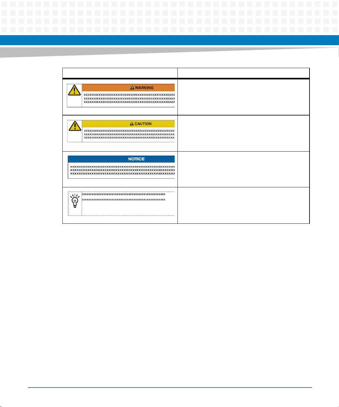
About this Manual
Indicates a hazardous situation which, if not avoided,
could result in death or serious injury
Indicates a hazardous situation which, if not avoided,
may result in minor or moderate injury
Indicates a property damage message
No danger encountered. Pay attention to important
information
16
MVME55006E Single Board Computer Installation and Use (6806800A37J)

Summary of Changes
This manual has been revised and replaces all prior editions.
Date Change Replaces
About this Manual
January 2007 Default setting for J102 - J110 is [1-2] (see Figure 1-3 on page
29).
February 2007 Default setting for J32 is [1-2]
Default setting for J28 is [1-2}
PMC Mode for J28 and J32 is factory default
P2 PMC 2 I/O mode for J102-J110 is factory default
P2 IPMC I/O is [2-3]
See Figure 1-4 on page 30 and Figure 1-5 on page 30.
March 2008 Updated to Emerson style standards. 6806800A37C
October 2008 Updated Table 1-2 on page 23 to correctly identify the
default setting for Jumpers J28, J32 as PMC mode by putting
brackets around 1-2 on both in the Settings column.
August 2011 Added Safety Notes on page 133 and Sicherheitshinweise on
page 137.
December 2012 Added Declaration of Conformity on page 20. 6806800A37G
September 2013 Updated L3 Cache on page 49, Intel Ethernet Controller
82544EI replaced with 82545GM.
July 2014 Re branded to Artesyn template. 6806800A37J
6806800A37A
6806800A37B
6806800A37D
6806800A37E
6806800A37H
MVME55006E Single Board Computer Installation and Use (6806800A37J)
17

About this Manual
About this Manual
18
MVME55006E Single Board Computer Installation and Use (6806800A37J)

Hardware Preparation and Installation
1.1 Overview
This chapter contains the following information:
Board and accessory preparation and installation instructions
ESD precautionary notes
1.2 Introduction
The MVME5500 is a single-board computer based on the PowerPC MPC7457 processor and the
Marvell GT-64260B host bridge with a dual PCI interface and memory controller. On-board
payload includes two PMC slots, two SDRAM banks, an expansion connector for two additional
banks of SDRAM, 8MB boot Flash ROM, one 10/100/1000 Ethernet port, one 10/100 Ethernet
port, 32MB expansion Flash ROM, two serial ports, NVRAM and a real-time clock.
Chapter 1
The MVME5500 interfaces to a VMEbus system via its P1 and P2 connectors and contains two
IEEE 1386.1 PCI mezzanine card (PMC) slots. The PMC slots are 64-bit and support both front
and rear I/O.
Additionally, the MVME5500 is user-configurable by setting on-board jumpers. Two I/O modes
are possible: PMC mode or SBC mode (also called 761 or IPMC mode). The SBC mode uses the
IPMC712 I/O PMC and the MVME712M transition module, or the IPMC761 I/O PMC and the
MVME761 transition module. The SBC mode is backwards compatible with the MVME761
transition module and the P2 adapter card (excluding PMC I/O routing) used on the
MVME5100 product. This mode is accomplished by configuring the on-board jumpers and by
attaching an IPMC761 PMC in PMC slot 1. Secondary Ethernet is configured to the rear.
PMC mode is backwards compatible with the MVME5100 and is accomplished by configuring
the on-board jumpers.
MVME55006E Single Board Computer Installation and Use (6806800A37J)
19

Hardware Preparation and Installation
1.3 Declaration of Conformity
Figure 1-1 Declaration of Conformity
E
C Declaration of Conformity
According to EN 17050-1:2004
Manufacturer’s Name:
Manufacturer’s Address:
Declares that the following product, in accordance with the requirements of 2004/108/EC, 2006/95/EC,
2011/65/EU and their amending directives,
Product:
Artesyn Embedded Technologies
Embedded Computing
Zhongshan General Carton Box Factory Co. Ltd. No 62, Qi
Guan Road West, Shiqi District, 528400 Zhongshan City
Guangdong, PRC
MVME5500 Series VMEbus Single Board Computer
Model Name/Number:
has been designed and manufactured to the following specifications:
EN55022:2006 (A1: 2007) Class A
EN55024: 1998 (A1: 2001 + A2: 2003)
2011/65/EU RoHS Directive
As manufacturer we hereby declare that the product named above has been designed to comply with the relevant sections of the above referenced specifications. This product complies with the essential health and safety
requirements of the above specified directives. We have an internal production control system that ensures
compliance between the manufactured products and the technical documentation.
___________________________________________________ ___
Tom Tuttle, Manager, Product Testing Services Date (MM/DD/YYYY)
MVME5500-0161, MVME5500-0163, MVME55005E-0163,
MVME55006E-0161, MVME55006E-0163
04/28/2014
______
20
MVME55006E Single Board Computer Installation and Use (6806800A37J)
Hardware Preparation and Installation
1.4 Getting Started
This section provides an overview of the steps necessary to install and power up the
MVME5500 and a brief section on unpacking and ESD precautions.
1.5 Overview of Startup Procedures
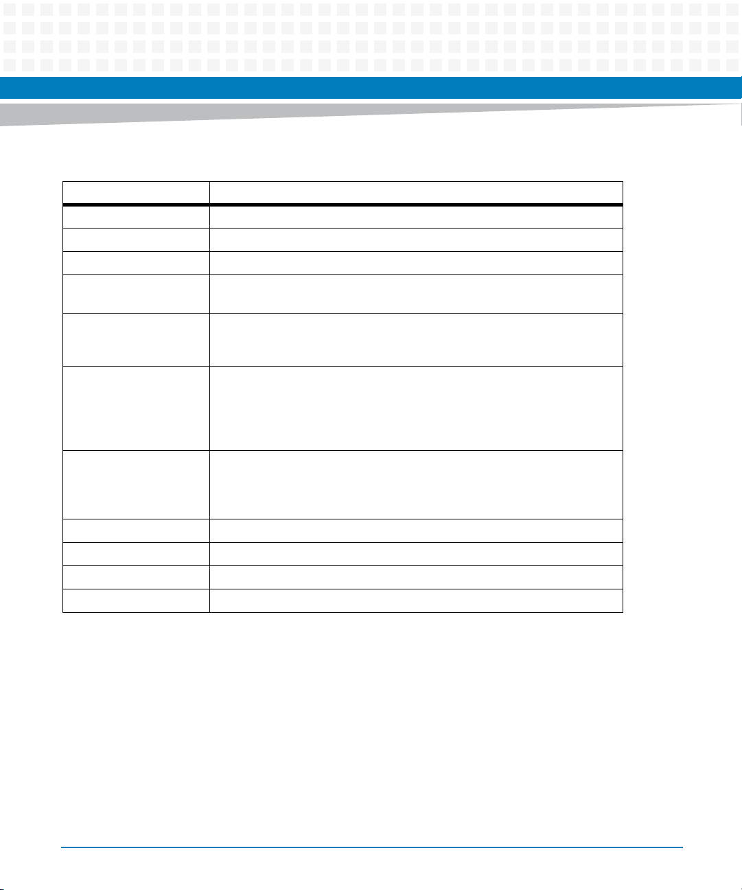
The following table lists the things you will need to do before you can use this board and tells
where to find the information you need to perform each step. Be sure to read this entire
chapter, including all Caution and Warning notes, before you begin.
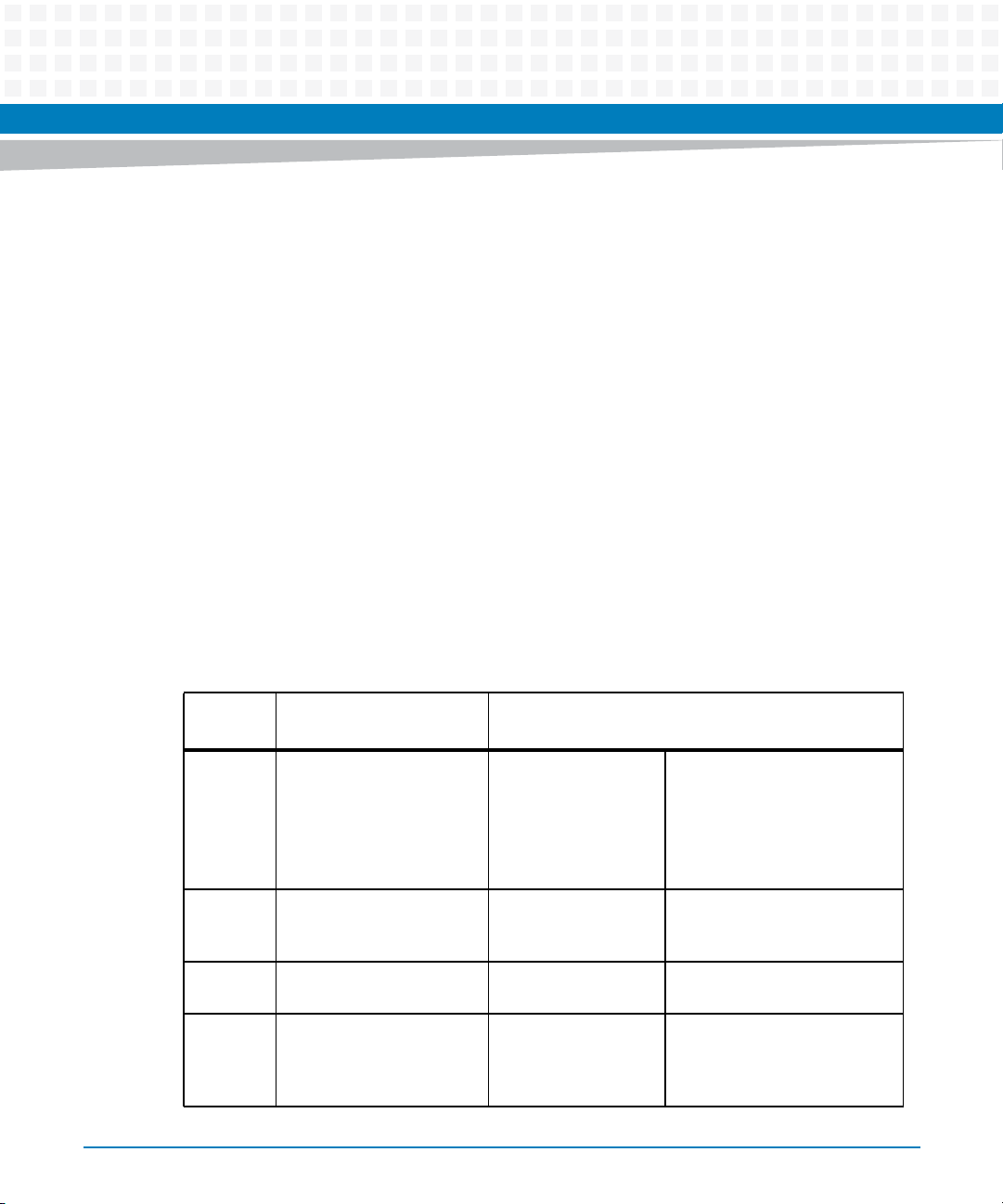
Table 1-1 Startup Overview
What you need to do... Refer to...
Unpack the hardware. Unpacking Guidelines on page 21
Configure the hardware by setting
jumpers on the board.
Install the MVME5500 board in a
chassis.
Connect any other equipment you will
be using
Verify the hardware is installed. Completing the Installation on page 45
Configuring the Board on page 23
Procedure on page 43
Connection to Peripherals on page 44
1.6 Unpacking Guidelines
Unpack the equipment from the shipping carton. Refer to the packing list and verify that all
items are present. Save the packing material for storing and reshipping of equipment.
MVME55006E Single Board Computer Installation and Use (6806800A37J)
21
Hardware Preparation and Installation
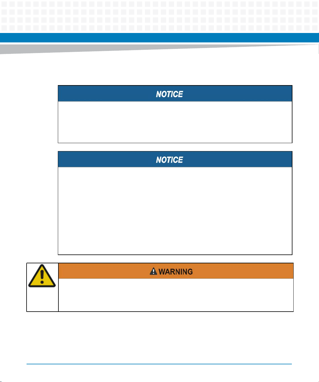
If the shipping carton is damaged upon receipt, request that the carrier’s agent be present
during the unpacking and inspection of the equipment.
Product Damage
Avoid touching areas of integrated circuitry; static discharge can damage circuits.
Inserting or removing modules with power applied may result in damage to module
components.
ESD
Artesyn strongly recommends that you use an antistatic wrist strap and a conductive foam
pad when installing or upgrading a system. Electronic components, such as disk drives,
computer boards, and memory modules can be extremely sensitive to electrostatic
discharge (ESD). After removing the component from its protective wrapper or from the
system, place the component flat on a grounded, static-free surface (and, in the case of a
board, component side up). Do not slide the component over any surface.
If an ESD station is not available, you can avoid damage resulting from ESD by wearing an
antistatic wrist strap (available at electronics stores) that is attached to an active electrical
ground. Note that a system chassis may not be grounded if it is unplugged.
Personal Injury or Death
Dangerous voltages, capable of causing death, are present in this equipment.
Use extreme caution when handling, testing, and adjusting.
1.7 Configuring the Hardware
This section discusses certain hardware and software tasks that may need to be performed
prior to installing the board in a chassis.
22
MVME55006E Single Board Computer Installation and Use (6806800A37J)
To produce the desired configuration and ensure proper operation of the MVME5500, you may
need to carry out certain hardware modifications before installing the module.
Most options on the MVME5500 are software configurable. Configuration changes are made
by setting bits in control registers after the board is installed in a system.
Jumpers and switches are used to control those options that are not software configurable.
These settings are described further on in this section. If you are resetting the board jumpers
or switches from their default settings, it is important to verify that all settings are reset
properly.
1.7.1 Configuring the Board
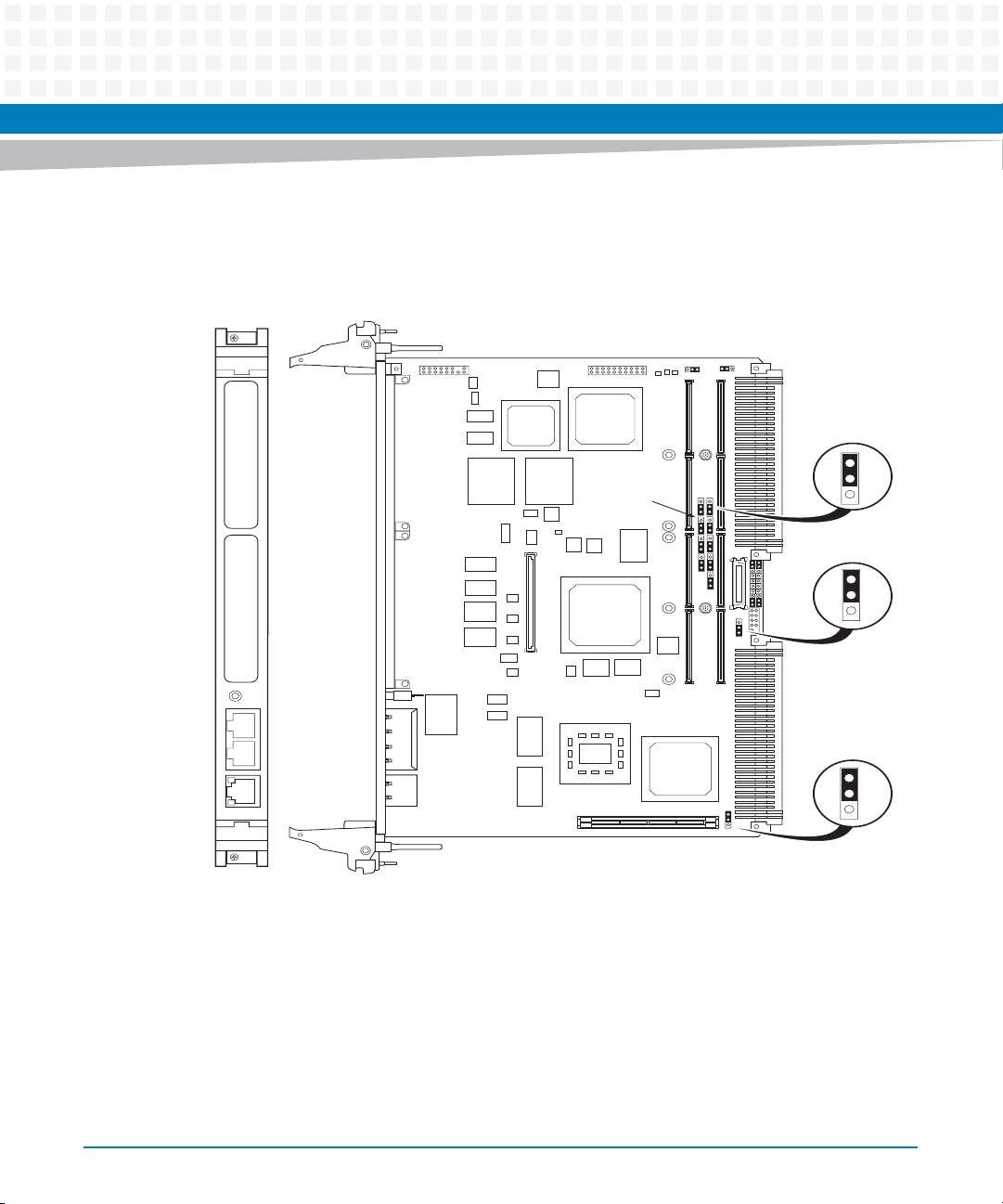
Figure 1-2 illustrates the placement of the jumpers, headers, switches, connectors, and various
other components on the MVME5500. There are several manually configurable headers and
switches on the MVME5500 and their settings are shown in Table 1-2. Each default setting is
enclosed in brackets. For pin assignments on the MVME5500, refer to Chapter 5, Connector Pin
Assignments.
Hardware Preparation and Installation
Table 1-2 MVME5500 Jumper Settings
Jumpers /
Switches Function
J6, J100,
J7, J101
J8 Flash Boot Bank Select
S3-1 Flash 0 Programming
S5-1 Safe Start ENV Header [OFF]
MVME55006E Single Board Computer Installation and Use (6806800A37J)
Ethernet 2 Selection
Headers
(see also J34, J97, J98, J99)
Refer to the hint on page 7
for a configuration
limitation.
Header
Enable Header
Settings
2-3 on all
[1-2 on all]
No jumper installed
[1-2]
2-3
OFF
[ON]
ON
Rear P2 Ethernet (SBC mode)
Front-panel Ethernet
Boots from Flash 0
Boots from Flash 0
Boots from Flash 1
Disables Flash 0 writes
Enables Flash 0 writes
Normal ENV settings used
during boot
Safe ENV settings used during
boot
23

Hardware Preparation and Installation
Table 1-2 MVME5500 Jumper Settings (continued)
Jumpers /
Switches Function
S3-2 Flash 0 Block Write Protect
Header
S3-4 Non-Standard Option
Header
S5-2 SROM Initialization Enable
Switch
S4-1 PCI Bus 0.0 Speed Header [OFF]
J27 VME SCON Select Header No jumper installed
J28, J32 PMC/SBC Mode Selection
Headers
(set both jumpers)
Refer to PMC/SBC Mode
Selection on page 27 for a
notice about configuring
for IPMC mode.
Settings
OFF
[ON]
[OFF] For factory use only
OFF
[ON]
ON
1-2
[2-3]
[1-2 on both]
2-3 on both
1-2 on J28
2-3 on J32
Disables Flash 0 J3 block writes
Enables Flash 0 J3 block writes
Enables SROM initialization
Disables SROM initialization
PMC board controls whether
the bus runs at 33 MHz or
66 MHz
Forces PCI bus 0.0 to remain at
33 MHz
Always SCON
No SCON
Auto-SCON
PMC mode
SBC/IPMC761 mode
SBC/IPMC712 mode
24
S4-2 PCI Bus 1.0 Speed Header [OFF]
ON
S3-3 EEPROM Write Protect
Header
MVME55006E Single Board Computer Installation and Use (6806800A37J)
OFF
[ON]
PMC board controls whether
the bus runs at 33 MHz or 66
MHz.
Forces PCI bus 1.0 to remain at
33 MHz.
Disables EEPROM
programming
Enables EEPROM
programming
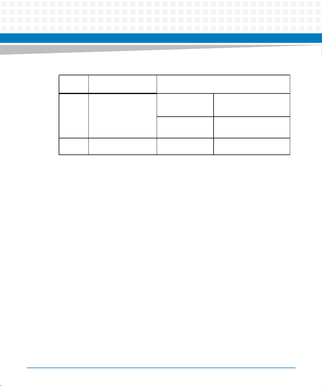
Hardware Preparation and Installation
Table 1-2 MVME5500 Jumper Settings (continued)
Jumpers /
Switches Function
J34, J97,
J98, J99
J102 –
J110
Ethernet 2 Selection
Headers
(see also J6, J100, J7, J101)
Refer to a note on page 27
for a configuration
limitation.
P2 I/O Selection Headers 1-2
Settings
1-2 on all Rear P2 Ethernet
[No jumpers installed] Front-panel Ethernet
[2-3]
Items in brackets are factory default settings.
(set when in SBC/IPMC761
mode)
PMC 2 I/O connected to P2
IPMC I/O connected to P2
MVME55006E Single Board Computer Installation and Use (6806800A37J)
25
Hardware Preparation and Installation
The MVME5500 is factory tested and shipped with the configuration described in the following
section.
Figure 1-2 MVME5500 Board Layout
PMC 2
PMC 1
ABT/RST
GigE
10/100 CPU BFL
4436 0207
ENET 2ENET 1
COM1
J5 J18
U7
U6
U5
U4
XU2 XU1
U15
U14
U13
U12
U11
U3
U10
U2
U9
U8
S2
U1
S1
J2
J1
U123
U124
J8
J4
S5
U29
U28
J21 J22
J23 J24
J11
J13 J14
U26
U31
U30
J27
J102 - J110
P1
J3
J6 / J100
J99
J98
J34
J12
J28
J97
J101 / J7
J33
J32
P2
1
3
J32
1
3
J28
1
3
U19
U16
S4
U17
P4
U25
U23
U125
U24
J102 - J110
U27
U22
U126
S3
U18
U129
U20
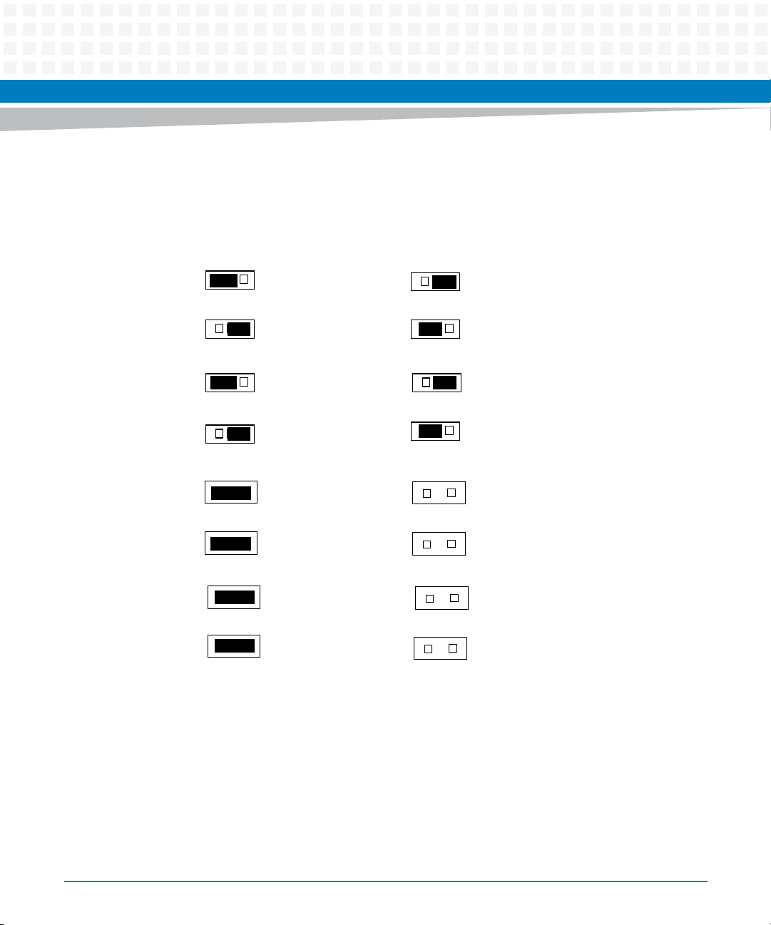
1.7.2 Ethernet 2, PMC/SBC Mode, and P2 I/O Selection Headers (J6, J7, J28, J32, J34, J97 – J110)
All of the headers described below are used in conjunction with each other to select various
modes of operation for 10/100BaseT Ethernet, PMC/SBC mode, and P2 I/O mode.
26
MVME55006E Single Board Computer Installation and Use (6806800A37J)

1.7.2.1 Ethernet
Four 3-pin planar headers (J6, J7, J100, J101) and four 2-pin planar headers (J34, J97, J98, J99)
are for 10/100/BaseT Ethernet 2 selection.
Ethernet 1 is the Gigabit Ethernet port and is front panel only.
For J6, J100, J7 and J101, install jumpers across pins 2-3 on all four headers for rear P2 Ethernet.
For front-panel Ethernet, install jumpers across pins 1-2 on all four headers.
If the rear P2 Ethernet is selected by jumpers J6, J7, J100, and J101, the Ethernet signals also
connect to PMC 1 user I/O connector J14. If a PMC card is plugged into PMC slot 1, there may be
a conflict between the I/O from the PMC card and the rear Ethernet signals. This conflict does not
occur with the IPMC761 or IPMC712 modules.
For J34, J97, J98 and J99, no jumpers are installed for front-panel Ethernet. For rear P2 Ethernet,
install jumpers across pins 1-2 on all four headers when in SBC/IPMC761 mode.
Hardware Preparation and Installation
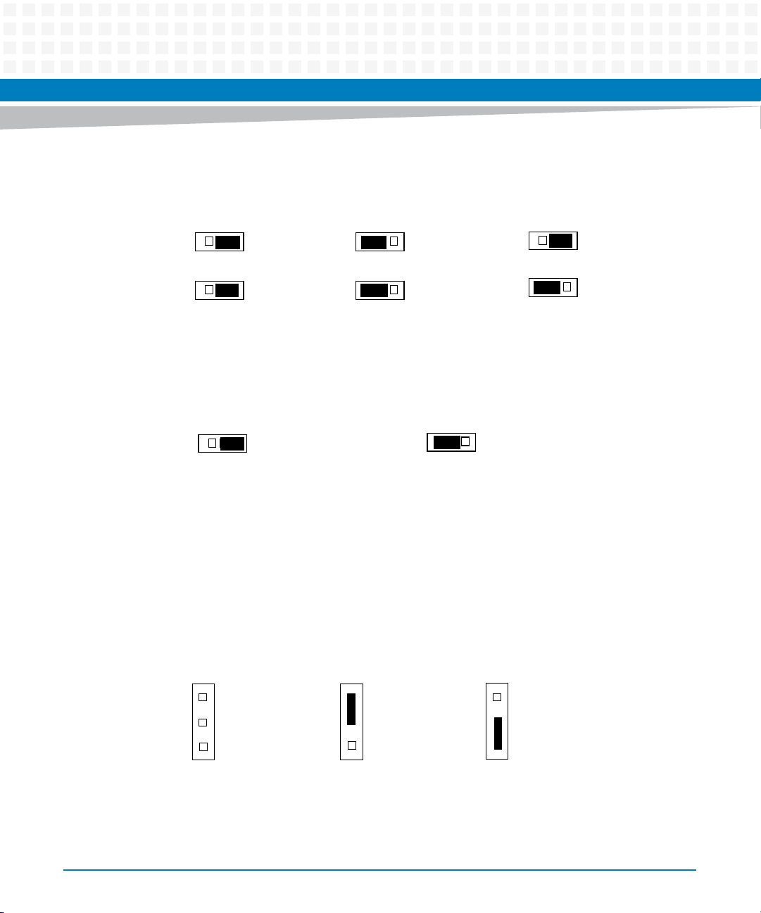
1.7.2.2 PMC/SBC Mode Selection
The MVME5500 is set at the factory for PMC mode. The SBC/IPMC761 mode should only be
selected when using the IPMC761 module in conjunction with the MVME761 transition
module. The PMC mode should be selected when using PMC modules with specific user I/O in
conjunction with the corresponding transition module. PMC mode should also be selected
when using PrPMC modules.
MVME55006E Single Board Computer Installation and Use (6806800A37J)
27
Hardware Preparation and Installation
Two 3-pin planar headers (J28, J32) control the supply of +/- 12 volts to the P2 connector; one
or both of these voltages are required by the MVME712 or MVME761 module when operating
in SBC mode. For PMC mode, jumpers are installed across pins 1-2 on both headers. For
SBC/IPMC761 mode, install jumpers across pins 2-3 on both headers. For SBC/IPMC712 mode,
install a jumper across pins 2-3 for J32 and install a jumper across pins 1-2 for J28.
Product Damage
When J28 is configured for SBC/IPMC mode, –12V is supplied to P2 pin A30. If there is an
incompatible board plugged into this P2 slot, damage may occur.
When J32 is configured for SBC/IPMC mode, +12V is supplied to P2 pin C7. If there is an
incompatible board plugged into this P2 slot, damage may occur.
1.7.2.3 P2 I/O Selection
Nine 3-pin planar headers (J102 –J110) are for P2 I/O selection. Jumpers are installed across
pins 1-2 on all nine headers when in PMC mode. Install jumpers across pins 2-3 on all nine
headers when in SBC/IPMC761 or SBC/IPMC712 mode to connect the extended SCSI signals to
P2.
28
MVME55006E Single Board Computer Installation and Use (6806800A37J)
Hardware Preparation and Installation
Figure 1-3 Front Panel and Rear P2 Ethernet Settings
(factory configuration)
Rear P2 Ethernet
Front-Panel Ethernet
J6
321
J7
123
J100 J100
321
J101 J101
123
J34
1
2
J97
1
2
J98
1
2
J99
1
2
J6
J7
J34
J97
J98
J99
321
123
321
123
1
2
1
2
1
2
1
2
MVME55006E Single Board Computer Installation and Use (6806800A37J)
29
Hardware Preparation and Installation
Figure 1-4 J28 and J32 Settings
(factory configuration)
PMC Mode
SBC/IPMC761 Mode
SBC/IPMC712 Mode
J28
321
J32
321
J28
321
J32
321
Figure 1-5 J102 - J110 Settings
(factory configuration)
P2 PMC 2 I/O
J102 –
J110
321
(extended SCSI)
P2 IPMC I/O
J102 –
J110
1.7.3 Flash Boot Bank Select Header (J8)
A 3-pin planar header selects the boot Flash bank. No jumper or a jumper installed across pins
1-2 selects Flash 0 as the boot bank. A jumper installed across pins 2-3 selects Flash 1 as the
boot bank.
Figure 1-6 J8 Settings
J28
321
J32
321
321
30
J8
1
2
3
Boots from Flash device 0
J8
1
2
3
Boots from Flash device 0Boots from Flash device 0
(factory configuration)
Boots from Flash device 1
J8
1
2
3
MVME55006E Single Board Computer Installation and Use (6806800A37J)
 Loading...