

Page 1

MVME4100 Single Board Computer
Installation and Use
P/N: 6806800H18G
June 2014
Page 2

©
Copyright 2014 Artesyn Embedded Technologies, Inc.
All rights reserved.
Trademarks
Artesyn Embedded Technologies, Artesyn and the Artesyn Embedded Technologies logo are trademarks and service marks of
Artesyn Embedded Technologies, Inc.© 2014 Artesyn Embedded Technologies, Inc. All other product or service names are the
property of their respective owners.
Intel® is a trademark or registered trademark of Intel Corporation or its subsidiaries in the United States and other countries.
Java™ and all other Java-based marks are trademarks or registered trademarks of Oracle America, Inc. in the U.S. and other countries.
Microsoft®, Windows® and Windows Me® are registered trademarks of Microsoft Corporation; and Windows XP™ is a trademark of
Microsoft Corporation.
PICMG®, CompactPCI®, AdvancedTCA™ and the PICMG, CompactPCI and AdvancedTCA logos are registered trademarks of the PCI
Industrial Computer Manufacturers Group.
UNIX® is a registered trademark of The Open Group in the United States and other countries.
Notice
While reasonable efforts have been made to assure the accuracy of this document, Artesyn assumes no liability resulting from any
omissions in this document, or from the use of the information obtained therein. Artesyn reserves the right to revise this document
and to make changes from time to time in the content hereof without obligation of Artesyn to notify any person of such revision or
changes.
Electronic versions of this material may be read online, downloaded for personal use, or referenced in another document as a URL to
an Artesyn website. The text itself may not be published commercially in print or electronic form, edited, translated, or otherwise
altered without the permission of Artesyn.
It is possible that this publication may contain reference to or information about Artesyn products (machines and programs),
programming, or services that are not available in your country. Such references or information must not be construed to mean that
Artesyn intends to announce such Artesyn products, programming, or services in your country.
Limited and Restricted Rights Legend
If the documentation contained herein is supplied, directly or indirectly, to the U.S. Government, the following notice shall apply
unless otherwise agreed to in writing by Artesyn.
Use, duplication, or disclosure by the Government is subject to restrictions as set forth in subparagraph (b)(3) of the Rights in
Technical Data clause at DFARS 252.227-7013 (Nov. 1995) and of the Rights in Noncommercial Computer Software and
Documentation clause at DFARS 252.227-7014 (Jun. 1995).
Contact Address
Artesyn Embedded Technologies Artesyn Embedded Technologies
Marketing Communications
2900 S. Diablo Way, Suite 190
Tempe, Arizona 85282
Lilienthalstr. 17-19
85579 Neubiberg/Munich
Germany
Page 3

Contents
Contents
About this Manual . . . . . . . . . . . . . . . . . . . . . . . . . . . . . . . . . . . . . . . . . . . . . . . . . . . . . . . . . . . . . . . . . . . . . . . 11
1 Introduction . . . . . . . . . . . . . . . . . . . . . . . . . . . . . . . . . . . . . . . . . . . . . . . . . . . . . . . . . . . . . . . . . . . . . . . . . 19
1.1 Features . . . . . . . . . . . . . . . . . . . . . . . . . . . . . . . . . . . . . . . . . . . . . . . . . . . . . . . . . . . . . . . . . . . . . . . . . . . 19
1.2 Standard Compliances . . . . . . . . . . . . . . . . . . . . . . . . . . . . . . . . . . . . . . . . . . . . . . . . . . . . . . . . . . . . . . 22
1.3 Mechanical Data . . . . . . . . . . . . . . . . . . . . . . . . . . . . . . . . . . . . . . . . . . . . . . . . . . . . . . . . . . . . . . . . . . . 24
1.4 Ordering Information . . . . . . . . . . . . . . . . . . . . . . . . . . . . . . . . . . . . . . . . . . . . . . . . . . . . . . . . . . . . . . . 24
1.4.1 Supported Board Models. . . . . . . . . . . . . . . . . . . . . . . . . . . . . . . . . . . . . . . . . . . . . . . . . . . . . . 24
1.4.2 Board Accessories . . . . . . . . . . . . . . . . . . . . . . . . . . . . . . . . . . . . . . . . . . . . . . . . . . . . . . . . . . . . 24
1.4.3 Serial Number Label . . . . . . . . . . . . . . . . . . . . . . . . . . . . . . . . . . . . . . . . . . . . . . . . . . . . . . . . . . 25
2 Hardware Preparation and Installation . . . . . . . . . . . . . . . . . . . . . . . . . . . . . . . . . . . . . . . . . . . . . . . . . 27
2.1 Overview . . . . . . . . . . . . . . . . . . . . . . . . . . . . . . . . . . . . . . . . . . . . . . . . . . . . . . . . . . . . . . . . . . . . . . . . . . 27
2.2 Unpacking and Inspecting the Board . . . . . . . . . . . . . . . . . . . . . . . . . . . . . . . . . . . . . . . . . . . . . . . . . . 28
2.3 Requirements . . . . . . . . . . . . . . . . . . . . . . . . . . . . . . . . . . . . . . . . . . . . . . . . . . . . . . . . . . . . . . . . . . . . . . 29
2.3.1 Environmental Requirements. . . . . . . . . . . . . . . . . . . . . . . . . . . . . . . . . . . . . . . . . . . . . . . . . . 29
2.3.2 Power Requirements . . . . . . . . . . . . . . . . . . . . . . . . . . . . . . . . . . . . . . . . . . . . . . . . . . . . . . . . . 30
2.3.3 Thermal Requirements . . . . . . . . . . . . . . . . . . . . . . . . . . . . . . . . . . . . . . . . . . . . . . . . . . . . . . . 31
2.3.4 Thermally Significant Components . . . . . . . . . . . . . . . . . . . . . . . . . . . . . . . . . . . . . . . . . . . . . 31
2.3.5 Equipment Requirements . . . . . . . . . . . . . . . . . . . . . . . . . . . . . . . . . . . . . . . . . . . . . . . . . . . . . 33
2.4 Configuring the Board . . . . . . . . . . . . . . . . . . . . . . . . . . . . . . . . . . . . . . . . . . . . . . . . . . . . . . . . . . . . . . 34
2.4.1 SMT Configuration Switch, S1 . . . . . . . . . . . . . . . . . . . . . . . . . . . . . . . . . . . . . . . . . . . . . . . . . 35
2.4.2 Geographical Address Switch, S2. . . . . . . . . . . . . . . . . . . . . . . . . . . . . . . . . . . . . . . . . . . . . . . 36
2.5 Installing Accessories . . . . . . . . . . . . . . . . . . . . . . . . . . . . . . . . . . . . . . . . . . . . . . . . . . . . . . . . . . . . . . . 38
2.5.1 Transition Module. . . . . . . . . . . . . . . . . . . . . . . . . . . . . . . . . . . . . . . . . . . . . . . . . . . . . . . . . . . . 38
2.5.2 PMC . . . . . . . . . . . . . . . . . . . . . . . . . . . . . . . . . . . . . . . . . . . . . . . . . . . . . . . . . . . . . . . . . . . . . . . . 39
2.5.3 XMCspan . . . . . . . . . . . . . . . . . . . . . . . . . . . . . . . . . . . . . . . . . . . . . . . . . . . . . . . . . . . . . . . . . . . 42
2.6 Installing and Removing the Board . . . . . . . . . . . . . . . . . . . . . . . . . . . . . . . . . . . . . . . . . . . . . . . . . . . . 43
2.7 Completing the Installation . . . . . . . . . . . . . . . . . . . . . . . . . . . . . . . . . . . . . . . . . . . . . . . . . . . . . . . . . . 44
2.8 Factory Installed Linux . . . . . . . . . . . . . . . . . . . . . . . . . . . . . . . . . . . . . . . . . . . . . . . . . . . . . . . . . . . . . . 45
3 Controls, LEDs, and Connectors . . . . . . . . . . . . . . . . . . . . . . . . . . . . . . . . . . . . . . . . . . . . . . . . . . . . . . . . 47
3.1 Overview . . . . . . . . . . . . . . . . . . . . . . . . . . . . . . . . . . . . . . . . . . . . . . . . . . . . . . . . . . . . . . . . . . . . . . . . . . 47
3.2 Board Layout . . . . . . . . . . . . . . . . . . . . . . . . . . . . . . . . . . . . . . . . . . . . . . . . . . . . . . . . . . . . . . . . . . . . . . . 48
MVME4100 Single Board Computer Installation and Use (6806800H18G)
3
Page 4

Contents
Contents
Contents
3.3 Front Panel . . . . . . . . . . . . . . . . . . . . . . . . . . . . . . . . . . . . . . . . . . . . . . . . . . . . . . . . . . . . . . . . . . . . . . . . 49
3.3.1 Reset/Abort Switch. . . . . . . . . . . . . . . . . . . . . . . . . . . . . . . . . . . . . . . . . . . . . . . . . . . . . . . . . . . 49
3.3.2 LEDs. . . . . . . . . . . . . . . . . . . . . . . . . . . . . . . . . . . . . . . . . . . . . . . . . . . . . . . . . . . . . . . . . . . . . . . . 50
3.3.3 Connectors. . . . . . . . . . . . . . . . . . . . . . . . . . . . . . . . . . . . . . . . . . . . . . . . . . . . . . . . . . . . . . . . . . 51
3.3.3.1 XMC Expansion Connector (J6) . . . . . . . . . . . . . . . . . . . . . . . . . . . . . . . . . . . . . . . 52
3.3.3.2 Ethernet Connectors (J4A/J4B) . . . . . . . . . . . . . . . . . . . . . . . . . . . . . . . . . . . . . . . . 54
3.3.3.3 PCI Mezzanine Card (PMC) Connectors (J11 – J14, J21 – J23) . . . . . . . . . . . . . . 54
3.3.3.4 Serial Port Connector (COM1/J1) . . . . . . . . . . . . . . . . . . . . . . . . . . . . . . . . . . . . . . 64
3.3.3.5 USB Connector (J2) . . . . . . . . . . . . . . . . . . . . . . . . . . . . . . . . . . . . . . . . . . . . . . . . . . 64
3.3.3.6 VMEbus P1 Connector . . . . . . . . . . . . . . . . . . . . . . . . . . . . . . . . . . . . . . . . . . . . . . . 65
3.3.3.7 VMEbus P2 Connector . . . . . . . . . . . . . . . . . . . . . . . . . . . . . . . . . . . . . . . . . . . . . . . 66
3.4 Headers . . . . . . . . . . . . . . . . . . . . . . . . . . . . . . . . . . . . . . . . . . . . . . . . . . . . . . . . . . . . . . . . . . . . . . . . . . . 67
3.4.1 Processor COP Header (P4). . . . . . . . . . . . . . . . . . . . . . . . . . . . . . . . . . . . . . . . . . . . . . . . . . . . 68
3.4.2 Boundary Scan Header (P5). . . . . . . . . . . . . . . . . . . . . . . . . . . . . . . . . . . . . . . . . . . . . . . . . . . . 68
4 Functional Description . . . . . . . . . . . . . . . . . . . . . . . . . . . . . . . . . . . . . . . . . . . . . . . . . . . . . . . . . . . . . . . . 71
4.1 Overview . . . . . . . . . . . . . . . . . . . . . . . . . . . . . . . . . . . . . . . . . . . . . . . . . . . . . . . . . . . . . . . . . . . . . . . . . . 71
4.2 Block Diagram . . . . . . . . . . . . . . . . . . . . . . . . . . . . . . . . . . . . . . . . . . . . . . . . . . . . . . . . . . . . . . . . . . . . . 72
4.3 Processor . . . . . . . . . . . . . . . . . . . . . . . . . . . . . . . . . . . . . . . . . . . . . . . . . . . . . . . . . . . . . . . . . . . . . . . . . . 73
4.4 I2C Serial Interface and Devices . . . . . . . . . . . . . . . . . . . . . . . . . . . . . . . . . . . . . . . . . . . . . . . . . . . . . . 73
4.5 System Memory . . . . . . . . . . . . . . . . . . . . . . . . . . . . . . . . . . . . . . . . . . . . . . . . . . . . . . . . . . . . . . . . . . . . 74
4.6 Timers . . . . . . . . . . . . . . . . . . . . . . . . . . . . . . . . . . . . . . . . . . . . . . . . . . . . . . . . . . . . . . . . . . . . . . . . . . . . 74
4.7 Ethernet Interfaces . . . . . . . . . . . . . . . . . . . . . . . . . . . . . . . . . . . . . . . . . . . . . . . . . . . . . . . . . . . . . . . . . 74
4.8 Local Bus Interface . . . . . . . . . . . . . . . . . . . . . . . . . . . . . . . . . . . . . . . . . . . . . . . . . . . . . . . . . . . . . . . . . . 75
4.8.1 Flash Memory . . . . . . . . . . . . . . . . . . . . . . . . . . . . . . . . . . . . . . . . . . . . . . . . . . . . . . . . . . . . . . . 75
4.8.2 NVRAM . . . . . . . . . . . . . . . . . . . . . . . . . . . . . . . . . . . . . . . . . . . . . . . . . . . . . . . . . . . . . . . . . . . . . 76
4.8.3 Quad UART (QUART) . . . . . . . . . . . . . . . . . . . . . . . . . . . . . . . . . . . . . . . . . . . . . . . . . . . . . . . . . 76
4.8.4 Control and Timers PLD . . . . . . . . . . . . . . . . . . . . . . . . . . . . . . . . . . . . . . . . . . . . . . . . . . . . . . . 76
4.9 DUART Interface . . . . . . . . . . . . . . . . . . . . . . . . . . . . . . . . . . . . . . . . . . . . . . . . . . . . . . . . . . . . . . . . . . . 77
4.10 PCI-X Port . . . . . . . . . . . . . . . . . . . . . . . . . . . . . . . . . . . . . . . . . . . . . . . . . . . . . . . . . . . . . . . . . . . . . . . . . 77
4.10.1 Tsi148 VME Controller . . . . . . . . . . . . . . . . . . . . . . . . . . . . . . . . . . . . . . . . . . . . . . . . . . . . . . . . 77
4.10.2 USB . . . . . . . . . . . . . . . . . . . . . . . . . . . . . . . . . . . . . . . . . . . . . . . . . . . . . . . . . . . . . . . . . . . . . . . . 77
4.11 XMC Expansion . . . . . . . . . . . . . . . . . . . . . . . . . . . . . . . . . . . . . . . . . . . . . . . . . . . . . . . . . . . . . . . . . . . . . 78
4.12 Power Supplies . . . . . . . . . . . . . . . . . . . . . . . . . . . . . . . . . . . . . . . . . . . . . . . . . . . . . . . . . . . . . . . . . . . . . 78
4.12.1 Power Sequencing . . . . . . . . . . . . . . . . . . . . . . . . . . . . . . . . . . . . . . . . . . . . . . . . . . . . . . . . . . . 78
4
MVME4100 Single Board Computer Installation and Use (6806800H18G)
Page 5

Contents
4.12.2 Power Supply Monitor . . . . . . . . . . . . . . . . . . . . . . . . . . . . . . . . . . . . . . . . . . . . . . . . . . . . . . . . 78
4.12.3 Power Supply Filtering and Fusing . . . . . . . . . . . . . . . . . . . . . . . . . . . . . . . . . . . . . . . . . . . . . . 78
4.13 Clock Distribution . . . . . . . . . . . . . . . . . . . . . . . . . . . . . . . . . . . . . . . . . . . . . . . . . . . . . . . . . . . . . . . . . . 79
4.13.1 System Clock . . . . . . . . . . . . . . . . . . . . . . . . . . . . . . . . . . . . . . . . . . . . . . . . . . . . . . . . . . . . . . . . 79
4.13.2 Real Time Clock Input. . . . . . . . . . . . . . . . . . . . . . . . . . . . . . . . . . . . . . . . . . . . . . . . . . . . . . . . . 79
4.13.3 Local Bus Controller Clock Divisor . . . . . . . . . . . . . . . . . . . . . . . . . . . . . . . . . . . . . . . . . . . . . . 79
4.14 Reset Control Logic . . . . . . . . . . . . . . . . . . . . . . . . . . . . . . . . . . . . . . . . . . . . . . . . . . . . . . . . . . . . . . . . . 79
4.15 Real Time Clock Battery . . . . . . . . . . . . . . . . . . . . . . . . . . . . . . . . . . . . . . . . . . . . . . . . . . . . . . . . . . . . . 80
4.16 Debug Support . . . . . . . . . . . . . . . . . . . . . . . . . . . . . . . . . . . . . . . . . . . . . . . . . . . . . . . . . . . . . . . . . . . . . 80
5 Transition Module . . . . . . . . . . . . . . . . . . . . . . . . . . . . . . . . . . . . . . . . . . . . . . . . . . . . . . . . . . . . . . . . . . . . 81
5.1 Overview . . . . . . . . . . . . . . . . . . . . . . . . . . . . . . . . . . . . . . . . . . . . . . . . . . . . . . . . . . . . . . . . . . . . . . . . . . 81
5.2 Transition Module Layout . . . . . . . . . . . . . . . . . . . . . . . . . . . . . . . . . . . . . . . . . . . . . . . . . . . . . . . . . . . . 82
5.3 Features . . . . . . . . . . . . . . . . . . . . . . . . . . . . . . . . . . . . . . . . . . . . . . . . . . . . . . . . . . . . . . . . . . . . . . . . . . . 83
5.4 SEEPROM Address Switch, S1 . . . . . . . . . . . . . . . . . . . . . . . . . . . . . . . . . . . . . . . . . . . . . . . . . . . . . . . . 84
5.5 Rear Panel Connectors . . . . . . . . . . . . . . . . . . . . . . . . . . . . . . . . . . . . . . . . . . . . . . . . . . . . . . . . . . . . . . 85
5.5.1 MVME7216E PMC I/O Module (PIM) Connectors (J10, J14). . . . . . . . . . . . . . . . . . . . . . . . . 87
5.5.2 Ethernet Connectors (GIGE/J41B, GIGE/J2B,GIGE/J2A) . . . . . . . . . . . . . . . . . . . . . . . . . . . . 89
5.5.3 Serial Port Connectors (COM1/J41A, COM2–COM5/J2A-D) . . . . . . . . . . . . . . . . . . . . . . . . 89
5.6 PMC Input/Output Module . . . . . . . . . . . . . . . . . . . . . . . . . . . . . . . . . . . . . . . . . . . . . . . . . . . . . . . . . . 90
6 MOTLoad Firmware. . . . . . . . . . . . . . . . . . . . . . . . . . . . . . . . . . . . . . . . . . . . . . . . . . . . . . . . . . . . . . . . . . . 93
6.1 Overview . . . . . . . . . . . . . . . . . . . . . . . . . . . . . . . . . . . . . . . . . . . . . . . . . . . . . . . . . . . . . . . . . . . . . . . . . . 93
6.2 Implementation and Memory Requirements . . . . . . . . . . . . . . . . . . . . . . . . . . . . . . . . . . . . . . . . . . . 93
6.3 MOTLoad Commands . . . . . . . . . . . . . . . . . . . . . . . . . . . . . . . . . . . . . . . . . . . . . . . . . . . . . . . . . . . . . . . 93
6.3.1 Utilities . . . . . . . . . . . . . . . . . . . . . . . . . . . . . . . . . . . . . . . . . . . . . . . . . . . . . . . . . . . . . . . . . . . . . 93
6.3.2 Tests . . . . . . . . . . . . . . . . . . . . . . . . . . . . . . . . . . . . . . . . . . . . . . . . . . . . . . . . . . . . . . . . . . . . . . . 94
6.3.3 Command List . . . . . . . . . . . . . . . . . . . . . . . . . . . . . . . . . . . . . . . . . . . . . . . . . . . . . . . . . . . . . . . 95
6.4 Using the Command Line Interface . . . . . . . . . . . . . . . . . . . . . . . . . . . . . . . . . . . . . . . . . . . . . . . . . .100
6.4.1 Rules . . . . . . . . . . . . . . . . . . . . . . . . . . . . . . . . . . . . . . . . . . . . . . . . . . . . . . . . . . . . . . . . . . . . . .102
6.4.2 Help . . . . . . . . . . . . . . . . . . . . . . . . . . . . . . . . . . . . . . . . . . . . . . . . . . . . . . . . . . . . . . . . . . . . . . .102
6.5 Firmware Settings . . . . . . . . . . . . . . . . . . . . . . . . . . . . . . . . . . . . . . . . . . . . . . . . . . . . . . . . . . . . . . . . . 103
6.5.1 Default VME Settings . . . . . . . . . . . . . . . . . . . . . . . . . . . . . . . . . . . . . . . . . . . . . . . . . . . . . . . . 103
6.5.2 Control Register/Control Status Register Settings . . . . . . . . . . . . . . . . . . . . . . . . . . . . . . . 107
MVME4100 Single Board Computer Installation and Use (6806800H18G)
5
Page 6

Contents
Contents
Contents
6.5.3 Displaying VME Settings . . . . . . . . . . . . . . . . . . . . . . . . . . . . . . . . . . . . . . . . . . . . . . . . . . . . .107
6.5.4 Editing VME Settings . . . . . . . . . . . . . . . . . . . . . . . . . . . . . . . . . . . . . . . . . . . . . . . . . . . . . . . . 108
6.5.5 Deleting VME Settings . . . . . . . . . . . . . . . . . . . . . . . . . . . . . . . . . . . . . . . . . . . . . . . . . . . . . . . 108
6.5.6 Restoring Default VME Settings . . . . . . . . . . . . . . . . . . . . . . . . . . . . . . . . . . . . . . . . . . . . . . .109
6.6 Remote Start . . . . . . . . . . . . . . . . . . . . . . . . . . . . . . . . . . . . . . . . . . . . . . . . . . . . . . . . . . . . . . . . . . . . . 109
6.7 Boot Images . . . . . . . . . . . . . . . . . . . . . . . . . . . . . . . . . . . . . . . . . . . . . . . . . . . . . . . . . . . . . . . . . . . . . . 110
6.7.1 Checksum Algorithm . . . . . . . . . . . . . . . . . . . . . . . . . . . . . . . . . . . . . . . . . . . . . . . . . . . . . . . . 111
6.7.2 Image Flags . . . . . . . . . . . . . . . . . . . . . . . . . . . . . . . . . . . . . . . . . . . . . . . . . . . . . . . . . . . . . . . . 112
6.7.3 User Images . . . . . . . . . . . . . . . . . . . . . . . . . . . . . . . . . . . . . . . . . . . . . . . . . . . . . . . . . . . . . . . . 113
6.7.4 Alternate Boot Data Structure . . . . . . . . . . . . . . . . . . . . . . . . . . . . . . . . . . . . . . . . . . . . . . . .113
6.7.5 Alternate Boot Images and Safe Start . . . . . . . . . . . . . . . . . . . . . . . . . . . . . . . . . . . . . . . . . . 114
6.7.6 Boot Image Firmware Scan . . . . . . . . . . . . . . . . . . . . . . . . . . . . . . . . . . . . . . . . . . . . . . . . . . . 114
6.8 Startup Sequence . . . . . . . . . . . . . . . . . . . . . . . . . . . . . . . . . . . . . . . . . . . . . . . . . . . . . . . . . . . . . . . . . 115
A Battery Exchange. . . . . . . . . . . . . . . . . . . . . . . . . . . . . . . . . . . . . . . . . . . . . . . . . . . . . . . . . . . . . . . . . . . . 117
A.1 Battery Exchange . . . . . . . . . . . . . . . . . . . . . . . . . . . . . . . . . . . . . . . . . . . . . . . . . . . . . . . . . . . . . . . . . . 117
B sRelated Documentation . . . . . . . . . . . . . . . . . . . . . . . . . . . . . . . . . . . . . . . . . . . . . . . . . . . . . . . . . . . . . 119
B.1 Artesyn Embedded Technologies - Embedded Computing Documentation . . . . . . . . . . . . . . .119
B.2 Manufacturers Documents . . . . . . . . . . . . . . . . . . . . . . . . . . . . . . . . . . . . . . . . . . . . . . . . . . . . . . . . .119
B.3 Related Specifications . . . . . . . . . . . . . . . . . . . . . . . . . . . . . . . . . . . . . . . . . . . . . . . . . . . . . . . . . . . . . . 122
Safety Notes . . . . . . . . . . . . . . . . . . . . . . . . . . . . . . . . . . . . . . . . . . . . . . . . . . . . . . . . . . . . . . . . . . . . . . . . . . . .125
Sicherheitshinweise . . . . . . . . . . . . . . . . . . . . . . . . . . . . . . . . . . . . . . . . . . . . . . . . . . . . . . . . . . . . . . . . . . . . . 129
6
MVME4100 Single Board Computer Installation and Use (6806800H18G)
Page 7

List of Tables
Table 1-1 Features List . . . . . . . . . . . . . . . . . . . . . . . . . . . . . . . . . . . . . . . . . . . . . . . . . . . . . . . . . . . . . . . . . . . 19
Table 1-2 Board Standard Compliances . . . . . . . . . . . . . . . . . . . . . . . . . . . . . . . . . . . . . . . . . . . . . . . . . . . . 22
Table 1-3 Mechanical Data . . . . . . . . . . . . . . . . . . . . . . . . . . . . . . . . . . . . . . . . . . . . . . . . . . . . . . . . . . . . . . . 24
Table 1-4 Board Variants . . . . . . . . . . . . . . . . . . . . . . . . . . . . . . . . . . . . . . . . . . . . . . . . . . . . . . . . . . . . . . . . . 24
Table 2-1 Startup Overview . . . . . . . . . . . . . . . . . . . . . . . . . . . . . . . . . . . . . . . . . . . . . . . . . . . . . . . . . . . . . . 27
Table 2-2 MVME4100 Specifications . . . . . . . . . . . . . . . . . . . . . . . . . . . . . . . . . . . . . . . . . . . . . . . . . . . . . . 29
Table 2-3 Power Requirements . . . . . . . . . . . . . . . . . . . . . . . . . . . . . . . . . . . . . . . . . . . . . . . . . . . . . . . . . . . 30
Table 2-4 Thermally Significant Components . . . . . . . . . . . . . . . . . . . . . . . . . . . . . . . . . . . . . . . . . . . . . . . 31
Table 2-5 Configuration Switch Settings (S1) . . . . . . . . . . . . . . . . . . . . . . . . . . . . . . . . . . . . . . . . . . . . . . . 36
Table 2-6 Geographical Address Switch Settings . . . . . . . . . . . . . . . . . . . . . . . . . . . . . . . . . . . . . . . . . . . . 37
Table 3-1 Front Panel LEDs . . . . . . . . . . . . . . . . . . . . . . . . . . . . . . . . . . . . . . . . . . . . . . . . . . . . . . . . . . . . . . . 50
Table 3-2 Base Board Connectors . . . . . . . . . . . . . . . . . . . . . . . . . . . . . . . . . . . . . . . . . . . . . . . . . . . . . . . . . 51
Table 3-3 XMC Expansion Connector (J6) Pin Assignments . . . . . . . . . . . . . . . . . . . . . . . . . . . . . . . . . . . 52
Table 3-4 Ethernet Connectors (J4A/J4B) Pin Assignments . . . . . . . . . . . . . . . . . . . . . . . . . . . . . . . . . . . 54
Table 3-5 PMC Slot 1 Connector (J11) Pin Assignments . . . . . . . . . . . . . . . . . . . . . . . . . . . . . . . . . . . . . . 54
Table 3-6 PMC Slot 1 Connector (J12) Pin Assignments . . . . . . . . . . . . . . . . . . . . . . . . . . . . . . . . . . . . . . 56
Table 3-7 PMC Slot 1 Connector (J13) Pin Assignments . . . . . . . . . . . . . . . . . . . . . . . . . . . . . . . . . . . . . . 57
Table 3-8 PMC Slot 1 Connector (J14) Pin Assignments . . . . . . . . . . . . . . . . . . . . . . . . . . . . . . . . . . . . . . 58
Table 3-9 PMC Slot 2 Connector (J21) Pin Assignments . . . . . . . . . . . . . . . . . . . . . . . . . . . . . . . . . . . . . . 60
Table 3-10 PMC Slot 2 Connector (J22) Pin Assignments . . . . . . . . . . . . . . . . . . . . . . . . . . . . . . . . . . . . . . 61
Table 3-11 PMC Slot 2 Connector (J23) Pin Assignments . . . . . . . . . . . . . . . . . . . . . . . . . . . . . . . . . . . . . . 62
Table 3-12 COM1 Port Connector Pin Assignments . . . . . . . . . . . . . . . . . . . . . . . . . . . . . . . . . . . . . . . . . . . 64
Table 3-13 USB Connector (J2) Pin Assignments . . . . . . . . . . . . . . . . . . . . . . . . . . . . . . . . . . . . . . . . . . . . . 64
Table 3-14 VMEbus P1 Connector Pin Assignments . . . . . . . . . . . . . . . . . . . . . . . . . . . . . . . . . . . . . . . . . . . 65
Table 3-15 VME P2 Connector Pinouts . . . . . . . . . . . . . . . . . . . . . . . . . . . . . . . . . . . . . . . . . . . . . . . . . . . . . . 66
Table 3-16 Processor COP Header (P4) Pin Assignments . . . . . . . . . . . . . . . . . . . . . . . . . . . . . . . . . . . . . . . 68
Table 3-17 Boundary Scan Header (P5) Pin Assignments . . . . . . . . . . . . . . . . . . . . . . . . . . . . . . . . . . . . . . 68
Table 4-1 Clock Frequencies . . . . . . . . . . . . . . . . . . . . . . . . . . . . . . . . . . . . . . . . . . . . . . . . . . . . . . . . . . . . . . 79
Table 5-1 Transition Module Features . . . . . . . . . . . . . . . . . . . . . . . . . . . . . . . . . . . . . . . . . . . . . . . . . . . . . . 83
Table 5-2 SEEPROM Address Switch Assignments (RTM) . . . . . . . . . . . . . . . . . . . . . . . . . . . . . . . . . . . . . 84
Table 5-3 Switch Settings and Device Addresses . . . . . . . . . . . . . . . . . . . . . . . . . . . . . . . . . . . . . . . . . . . . 84
Table 5-4 Transition Module Connectors . . . . . . . . . . . . . . . . . . . . . . . . . . . . . . . . . . . . . . . . . . . . . . . . . . . 85
Table 5-5 Transition Module LEDs . . . . . . . . . . . . . . . . . . . . . . . . . . . . . . . . . . . . . . . . . . . . . . . . . . . . . . . . . 87
Table 5-6 MVME721 Host I/O Connector (J10) Pin Assignments . . . . . . . . . . . . . . . . . . . . . . . . . . . . . . . 87
Table 5-7 Ethernet Connectors Pin Assignment . . . . . . . . . . . . . . . . . . . . . . . . . . . . . . . . . . . . . . . . . . . . . 89
Table 5-8 COM Port Connector Pin Assignments . . . . . . . . . . . . . . . . . . . . . . . . . . . . . . . . . . . . . . . . . . . . 89
MVME4100 Single Board Computer Installation and Use (6806800H18G)
7
Page 8

List of Tables
Table 6-1 MOTLoad Commands . . . . . . . . . . . . . . . . . . . . . . . . . . . . . . . . . . . . . . . . . . . . . . . . . . . . . . . . . . . 95
Table 6-2 MOTLoad Image Flags . . . . . . . . . . . . . . . . . . . . . . . . . . . . . . . . . . . . . . . . . . . . . . . . . . . . . . . . .112
Table B-1 Artesyn Embedded Technologies - Embedded Computing Publications . . . . . . . . . . . . . .119
Table B-2 Manufacturer’s Publications . . . . . . . . . . . . . . . . . . . . . . . . . . . . . . . . . . . . . . . . . . . . . . . . . . . .119
Table B-3 Related Specifications . . . . . . . . . . . . . . . . . . . . . . . . . . . . . . . . . . . . . . . . . . . . . . . . . . . . . . . . .122
8
MVME4100 Single Board Computer Installation and Use (6806800H18G)
Page 9

List of Figures
Figure 1-1 Declaration of Conformity . . . . . . . . . . . . . . . . . . . . . . . . . . . . . . . . . . . . . . . . . . . . . . . . 23
Figure 1-2 Serial Number Label Location . . . . . . . . . . . . . . . . . . . . . . . . . . . . . . . . . . . . . . . . . . . . . 25
Figure 2-1 Primary Side Thermally Significant Components . . . . . . . . . . . . . . . . . . . . . . . . . . . . 32
Figure 2-2 Secondary Side Thermally Significant Components . . . . . . . . . . . . . . . . . . . . . . . . . . 33
Figure 2-3 Switch Locations . . . . . . . . . . . . . . . . . . . . . . . . . . . . . . . . . . . . . . . . . . . . . . . . . . . . . . . . 34
Figure 2-4 SMT Configuration Switch Position . . . . . . . . . . . . . . . . . . . . . . . . . . . . . . . . . . . . . . . . 35
Figure 2-5 Geographical Address Switch Position . . . . . . . . . . . . . . . . . . . . . . . . . . . . . . . . . . . . . 37
Figure 2-6 Typical Placement of a PMC Module on a VME Module . . . . . . . . . . . . . . . . . . . . . . . 42
Figure 3-1 Component Layout . . . . . . . . . . . . . . . . . . . . . . . . . . . . . . . . . . . . . . . . . . . . . . . . . . . . . . 48
Figure 3-2 Front Panel LEDs, Connectors, Switch . . . . . . . . . . . . . . . . . . . . . . . . . . . . . . . . . . . . . . 49
Figure 4-1 Block Diagram . . . . . . . . . . . . . . . . . . . . . . . . . . . . . . . . . . . . . . . . . . . . . . . . . . . . . . . . . . 72
Figure 5-1 Component Layout . . . . . . . . . . . . . . . . . . . . . . . . . . . . . . . . . . . . . . . . . . . . . . . . . . . . . . 82
Figure 5-2 Block Diagram . . . . . . . . . . . . . . . . . . . . . . . . . . . . . . . . . . . . . . . . . . . . . . . . . . . . . . . . . . 83
Figure 5-3 S1 Switch Positions . . . . . . . . . . . . . . . . . . . . . . . . . . . . . . . . . . . . . . . . . . . . . . . . . . . . . . 84
Figure 5-4 Rear Panel Connectors and LEDs . . . . . . . . . . . . . . . . . . . . . . . . . . . . . . . . . . . . . . . . . . 86
Figure 5-5 Installing the PIM . . . . . . . . . . . . . . . . . . . . . . . . . . . . . . . . . . . . . . . . . . . . . . . . . . . . . . . 91
Figure A-1 Battery Location . . . . . . . . . . . . . . . . . . . . . . . . . . . . . . . . . . . . . . . . . . . . . . . . . . . . . . . 117
MVME4100 Single Board Computer Installation and Use (6806800H18G)
9
Page 10

List of Figures
10
MVME4100 Single Board Computer Installation and Use (6806800H18G)
Page 11

About this Manual
Overview of Contents
This manual provides the information required to install and configure an MVME4100 Single
Board Computer. Additionally, this manual provides specific preparation and installation
information and data applicable to the board.
The MVME4100 single-board computer, with the Freescale MPC8548E system-on-chip (SoC)
processor, provides a high-performance, cost-effective continuation for currently deployed
VME infrastructure.
This manual is divided into the following chapters and appendices:
Chapter 1, Introduction, lists the features of the MVME4100 base board, standard compliances,
and model numbers for boards and accessories.
Chapter 2, Hardware Preparation and Installation, includes a description of the MVME4100,
unpacking instructions, environmental, thermal, and power requirements, and how to prepare
and install the base board, transition module, and PMC module.
Chapter 3, Controls, LEDs, and Connectors, provides an illustration of the board components and
front panel details. This chapter also gives descriptions for the onboard and front panel LEDs
and connectors.
Chapter 4, Functional Description, describes the major features of the MVME4100 base board.
These descriptions include both programming and hardware characteristics of major
components.
Chapter 5, Transition Module, describes the MVME7216E transition module used with the
MVME4100.
Chapter 6, MOTLoad Firmware, describes the role, process and commands employed by the
MVME4100 diagnostic and initialization firmware MOTLoad. This chapter also briefly describes
how to use the debugger commands.
Appendix A, Battery Exchange, describes the procedure for replacing a battery.
Appendix B, sRelated Documentation, provides listings for publications, manufacturer’s
documents and related industry specification for this product.
Safety Notes, contains the cautions and warnings applicable to the use of this product.
Sicherheitshinweise, is a German translation of the Safety Notes chapter.
MVME4100 Single Board Computer Installation and Use (6806800H18G)
11
Page 12

About this Manual
Abbreviations
This document uses the following abbreviations:
Term Meaning
A/D Analog/Digital
ANSI American National Standard Institute
ASIC Application Specific Integrated Circuit
BGA Ball Grid Array
BLT Block Transfer
CCB Core Complex Bus
CE Chip Enable
CFM Cubic Feet per Minute
CHRP (PowerPC) Common Hardware Reference Platform
About this Manual
12
CMC Common Mezzanine Card
COM Communications
COP Common On-chip Processor
COTS Commercial-Off-the-Shelf
CRC Cyclic Redundancy Check
DDR Double Data Rate
DLL Delay-Locked Loop
DMA Direct Memory Access
DRAM Dynamic Random Access Memory
DUART Dual Universal Asynchronous Receiver/Transmitter
ECC Error Correction Code
EEPROM Electrically Erasable Programmable Read-Only Memory
EPROM Erasable Programmable Read-Only Memory
FCC Federal Communications Commission
FEC Fast Ethernet Controller
FIFO First In First Out
MVME4100 Single Board Computer Installation and Use (6806800H18G)
Page 13

Term Meaning
F/W Firmware
fpBGA Flip chip Plastic Ball Grid Array
GMII Gigabit Media Independent Interface
GPCM General Purpose Chip select Machine
GPR General Purpose Register
H/W Hardware
ID Identification
IDMA Independent Direct Memory Access
I/O Input/Output
IEEE Institute of Electrical and Electronics Engineers
I2C Inter IC
About this Manual
JTAG Joint Test Access Group
LBC Local Bus Controller
LCD Liquid Crystal Display
LED Light Emitting Diode
LSB Least Significant Byte
MBLT Multiplexed Block Transfer
MII Media Independent Interface
MSB Most Significant Byte
Msb Most Significant Bit
MTBF Mean Time Between Failure
NAND (Not and) Flash that is used for storage
NOR (Not or) Flash that is used for executing code
PBGA Plastic Ball Grid Array
PCI Peripheral Component Interconnect
PCI-X Peripheral Component Interconnect -X
PIC Programmable Interrupt Controller
PIM PCI Mezzanine Card Input/Output Module
MVME4100 Single Board Computer Installation and Use (6806800H18G)
13
Page 14

About this Manual
Term Meaning
PMC PCI Mezzanine Card (IEEE P1386.1)
PLD Programmable Logic Device
PLL Phase-Locked Loop
POR Power-On Reset
PRD Product Requirements Document
PReP PowerPC Reference Platform
PrPMC Processor PCI Mezzanine Card
QUART Quad Universal Asynchronous Receiver/Transmitter
Rcv Receive
RGMII Reduced Gigabit Media Independent Interface
RTBI Reduced Ten Bit Interface
RTC Real-Time Clock
About this Manual
14
RTM Rear Transition Module
sATA Serial AT Attachment
SBC Single Board Computer
SDRAM Synchronous Dynamic Random Access Memory
SMT Surface Mount Technology
SODIMM Small-Outline Dual In-line Memory Module
SPD Serial Presence Detect
SoC System-on-Chip
SRAM Static Random Access Memory
S/W Software
TBI Ten Bit Interface
TSEC Three-Speed Ethernet Controller
2eSST Two edge Source Synchronous Transfer
UART Universal Asynchronous Receiver/Transmitter
USB Universal Serial Bus
VIO Input/Output Voltage
MVME4100 Single Board Computer Installation and Use (6806800H18G)
Page 15
Term Meaning
VITA VMEbus International Trade Association
VME VMEbus (Versa Module Eurocard)
VPD Vital Product Data
Xmit Transmit
Conventions
The following table describes the conventions used throughout this manual.
Notation Description
0x00000000 Typical notation for hexadecimal numbers (digits are
About this Manual
0 through F), for example used for addresses and
offsets
0b0000 Same for binary numbers (digits are 0 and 1)
bold Used to emphasize a word
Screen Used for on-screen output and code related elements
or commands in body text
Courier + Bold Used to characterize user input and to separate it
from system output
Reference Used for references and for table and figure
descriptions
File > Exit Notation for selecting a submenu
<text> Notation for variables and keys
[text] Notation for software buttons to click on the screen
and parameter description
... Repeated item for example node 1, node 2, ..., node
12
.
.
.
.. Ranges, for example: 0..4 means one of the integers
Omission of information from example/command
that is not necessary at the time being
0,1,2,3, and 4 (used in registers)
MVME4100 Single Board Computer Installation and Use (6806800H18G)
15
Page 16
About this Manual
Notation Description
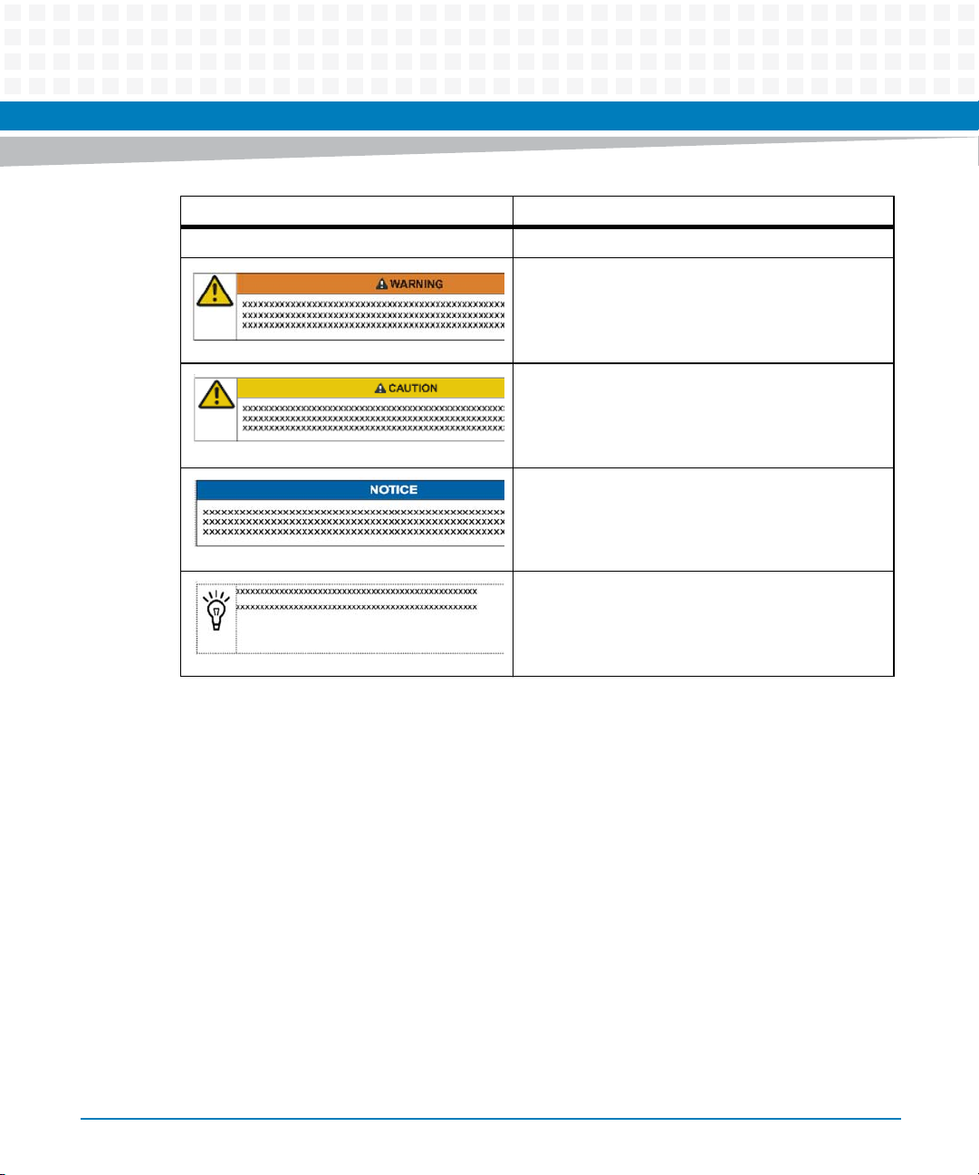
| Logical OR
About this Manual
Indicates a hazardous situation which, if not avoided,
could result in death or serious injury
Indicates a hazardous situation which, if not avoided,
may result in minor or moderate injury
Indicates a property damage message
No danger encountered. Pay attention to important
information
16
MVME4100 Single Board Computer Installation and Use (6806800H18G)
Page 17

Summary of Changes
Part Number Publication Date Description
6806800H18A January 2009 Early access version
6806800H18B April 2009 Update for final release, updated table "Feature List", added
6806800H18C June 2009 Corrected typo in section "Power Requirements"
6806800H18D June 2010 Minor updates to Table 1-1, "Features List"
About this Manual
"Declaration of Conformity", added section "Serial Number
Label", added weight of the board to section "Mechanical
Data", updated power requirements, added location of
thermally significant components, updated graphic of
switch location, updated connector pinouts, updated block
diagram, updated description of SEEPROM address switch,
editorial changes
Updated section 3.3.3 Connectors on page 51 and 5.5 Rear
Panel Connectors on page 85
6806800H18E March 2011 Corrected typo in section 2.8 Factory Installed Linux on page
45
6806800H18F August 2011 Updated Safety Notes on page 125 and Sicherheitshinweise
on page 129
6806800H18G June 2014 Re- branded to Artesyn template.
MVME4100 Single Board Computer Installation and Use (6806800H18G)
17
Page 18

About this Manual
About this Manual
18
MVME4100 Single Board Computer Installation and Use (6806800H18G)
Page 19

Introduction
1.1 Features
The MVME4100 Single Board Computer is a VMEbus board based on the MPC8548E Integrated
Processor. It is a full 6U board and occupies a single VME card slot with PMC cards installed. The
MVME4100 is compliant with the VITA standards VMEbus, 2eSST, and PCI-X as listed in
Appendix B, sRelated Documentation.
Target applications for this board are medical imaging, industrial control, radar/sonar, and test
and measure.
Table 1-1 Features List
Function Features
Chapter 1
Processor / Host Controller /
Memory Controller
System Memory One DDR2 SO-CDIMM for SDRAM with ECC
2
C One 8 KB VPD serial EEPROM
I
One MPC8548E Integrated Processor
One e500 core with integrated L2
Core frequency of 1.3 GHz
One integrated four channel DMA controller
One integrated PCI-E interface
One integrated PCI-X interface
Four integrated 10/100/1000 Ethernet controllers
One integrated DUART
2
Two integrated I
One integrated Programmable Interrupt Controller
One integrated Local Bus Controller
One integrated DDR2 SDRAM controller
2 GBytes
Up to DDR533
Two 64 KB user configuration serial EEPROMs
One Real Time Clock (RTC) with removable battery
Dual temperature sensor
One SPD for memory on SO-CDIMM
Connection to XMCspan and rear transition module
C controllers
MVME4100 Single Board Computer Installation and Use (6806800H18G)
19
Page 20

Introduction
Table 1-1 Features List (continued)
Function Features
Flash 128 MB soldered NOR flash with two alternate 1 MB boot sectors
NVRAM One 512 KB MRAM
PCI_E 8X Port to XMC Expansion
I/O One front panel mini DB-9 connector for front I/O: one serial channel
selectable via hardware switch
H/W switch or S/W bit write protection for entire logical bank
4 GB NAND flash
Two front panel RJ-45 connectors with integrated LEDs for front I/O:
two 10/100/1000 Ethernet channels
One front panel USB Type A upright receptacle for front I/O: one USB
2.0 channel
PMC site 1 front I/O and rear P2 I/O
PMC site 2 front I/O
USB One four-channel USB 2.0 controller: one channel for front panel I/O
Ethernet Four 10/100/1000 MPC8548E Ethernet channels: two front panel
Ethernet connectors and two channels for rear P2 I/O
Serial Interface One 16550-compatible, 9.6 to 115.2 Kbaud, MPC8548E,
asynchronous serial channel: one channel for front panel I/O
One quad UART (QUART) controller to provide four 16550-
compatible, 9.6 to 115.2 Kbaud, asynchronous serial channels: four
channels for rear P2 I/O
Timers Four 32-bit MPC8548E timers
Four 32-bit timers in a PLD
Watchdog Timer One watchdog timer in PLD
20
MVME4100 Single Board Computer Installation and Use (6806800H18G)
Page 21

Introduction
Table 1-1 Features List (continued)
Function Features
VME Interface VME64 (ANSI/VITA 1-1994) compliant (3 row backplane 96-pin VME
connector)
VME64 Extensions (ANSI/VITA 1.1-1997) compliant (5 row
backplane 160-pin VME connector)
2eSST (ANSI/VITA 1.5-2003) compliant
ANSI/VITA 1.7-2003 compliant (Increased Current Level for 96 pin &
160 pin DIN/IEC Connector Standard)
VITA 41.0, version 0.9 compliant
Two five-row P1 and P2 backplane connectors
One Tsi148 VMEbus controller
Form Factor Standard 6U VME, one slot
Miscellaneous One front panel RESET/ABORT switch
Six front panel status indicators:
Two 10/100/1000 Ethernet link/speed and activity (4 total)
Board fail
User S/W controlled LED
Planar status indicators
One standard 16-pin COP header
One standard 20-pin JTAG header
Boundary scan support
Switches for VME geographical addressing in a three-row backplane
Software Support VxWorks OS support
Linux OS support
MVME4100 Single Board Computer Installation and Use (6806800H18G)
21
Page 22

Introduction
1.2 Standard Compliances
The MVME4100 is designed to be CE compliant and to meet the following standard
requirements.
Table 1-2 Board Standard Compliances
Standard Description
UL 60950-1
EN 60950-1
IEC 60950-1
CAN/CSA C22.2 No 60950-1
CISPR 22
CISPR 24
EN 55022
EN 55024
FCC Part 15
Industry Canada ICES-003
VCCI Japan
AS/NZS CISPR 22
EN 300 386
NEBS Standard GR-1089 CORE
NEBS Standard GR-63-CORE
ETSI EN 300 019 series
Directive 2002/95/EC Directive on the restriction of the use of certain hazardous
Safety Requirements (legal)
EMC requirements (legal) on system level (predefined Artesyn
system)
Environmental Requirements
substances in electrical and electronic equipment (RoHS)
22
MVME4100 Single Board Computer Installation and Use (6806800H18G)
Page 23
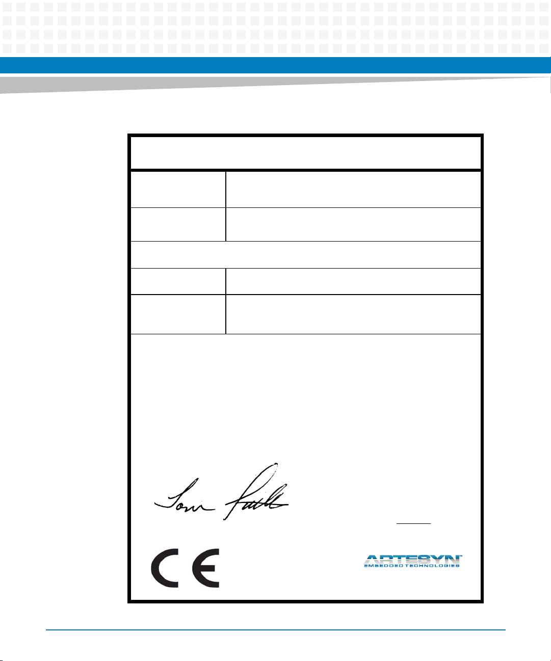
Figure 1-1 Declaration of Conformity
E
C Declaration of Conformity
According to EN 17050-1:2004
Introduction
Manufacturer’s Name:
Manufacturer’s Address:
Declares that the following product, in accordance with the requirements of 2004/108/EC, 2006/95/EC, 2011/65/
EU and their amending directives,
Product:
Model Name/Number:
has been designed and manufactured to the following specifications:
EN55022: 2006
EN55024 (A1: 2001 + A2: 2003): 1998
2011/65/EU RoHS Directive
As manufacturer we hereby declare that the product named above has been designed to comply with the relevant sections of the above referenced specifications. This product complies with the essential health and safety
requirements of the above specified directives. We have an internal production control system that ensures
compliance between the manufactured products and the technical documentation.
Artesyn Embedded Technologies
Embedded Computing
Zhongshan General Carton Box Factory Co. Ltd. No 62, Qi
Guan Road West, Shiqi District, 528400 Zhongshan City
Guangdong, PRC
MVME4100 VMEbus Single Board Computer Series
MVME4100-0171, MVME4100-0173
___________________________________________________ ___
Tom Tuttle, Manager, Product Testing Services Date (MM/DD/YYYY)
MVME4100 Single Board Computer Installation and Use (6806800H18G)
06/17/2014______
23
Page 24
Introduction
1.3 Mechanical Data
This section provides details on the board’s mechanical data.
Table 1-3 Mechanical Data
Characteristic Value
Dimensions (D x W x H) 6U, 4HP wide, (233.4 mm x 160 mm x 19.8 mm)
Weight 0.453 kg
1.4 Ordering Information
When ordering board variants or board accessories, use the order numbers given in the
following tables.
1.4.1 Supported Board Models
At the time of publication of this manual, the MVME4100 Single Board Computer is available in
the configurations shown below.
Table 1-4 Board Variants
Marketing Number Processor
MVME4100-0171 1.3 GHz MPC8548E, 4 GB NAND flash, 2 GB DDR2, Scanbe handles
MVME4100-0173 1.3 GHz MPC8548E, 4 GB NAND flash, 2 GB DDR2, IEEE handles
1.4.2 Board Accessories
This table lists the available expansion and transition modules for the MVME4100.
Model Number Description
MVME7216E-001 Transition module, 6E
XMCSPAN-001 XMC Expansion, IEEE handles
XMCSPAN-002 XMC Expansion, Scanbe handles
24
MVME4100 Single Board Computer Installation and Use (6806800H18G)
Page 25
The IPMC712 and IPMC761 I/O modules are not supported on the MVME4100.
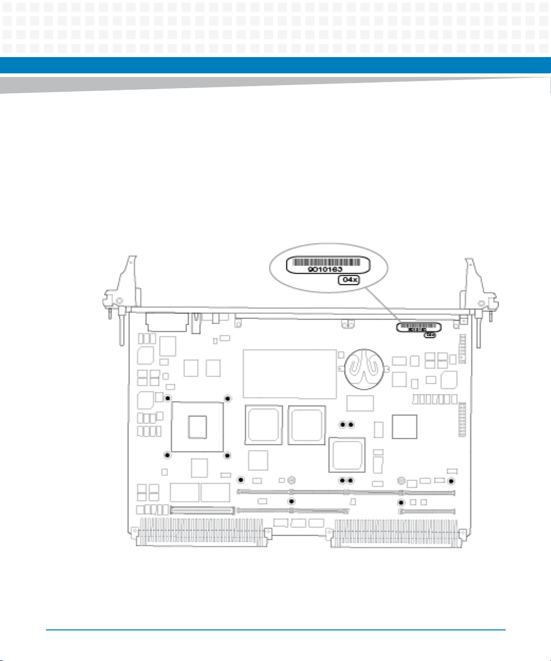
1.4.3 Serial Number Label
You can find the serial number of your product on a label that is located on the PCB close to the
front panel. The following figure shows a sample label and its location. The actual label on your
product may vary in content and location.
Figure 1-2 Serial Number Label Location
Introduction
MVME4100 Single Board Computer Installation and Use (6806800H18G)
25
Page 26

Introduction
26
MVME4100 Single Board Computer Installation and Use (6806800H18G)
Page 27
Hardware Preparation and Installation
2.1 Overview
This chapter provides startup and safety instructions related to this product, hardware
preparation instruction that includes default switch settings. System considerations and
installation instructions for the base board, PMC, and transition module are also described in
this chapter.
A fully implemented MVME4100 consists of the base board plus:
Two single-wide or one double-wide PCI Mezzanine Card (PMC) slot for added versatility.
One transition module for support of the mapped I/O from the MVME4100 base board to
the P2 connector.
Up to two optional XMCspan cards.
The following table lists the things you will need to do before you can use this board and tells
you where to find the information you need to perform each step. Be sure to read this entire
chapter, including all Caution and Warning notes, before you begin.
Chapter 2
Table 2-1 Startup Overview
Task Page
Unpack the hardware. Unpacking and Inspecting the Board on page 28
Configure the hardware by setting jumpers
on the board and RTM.
Install the MVME7216E transition module in
the chassis.
Install PMC module (if required). Installing Accessories on page 38
Install XMCspan module (if required). XMCspan Installation and Use manual (6806800H03)
Install the MVME4100 in the chassis. Installing and Removing the Board on page 43
Attach cabling and apply power. Completing the Installation on page 44
Install PIM on transition module (if
required).
Ensure that the firmware initializes the
MVME4100
Initialize the board Chapter 6, MOTLoad Firmware
MVME4100 Single Board Computer Installation and Use (6806800H18G)
Configuring the Board on page 34 and SEEPROM Address
Switch, S1 on page 84
Transition Module on page 38
PMC Input/Output Module on page 90
Chapter 6, MOTLoad Firmware
27
Page 28
Hardware Preparation and Installation
Table 2-1 Startup Overview (continued)
Task Page
Examine and/or change environmental
parameters.
MVME4100 Single Board Computer Programmer’s
Reference
Program the board as needed for your
applications.
MVME4100 Single Board Computer Programmer’s
Reference
2.2 Unpacking and Inspecting the Board
Read all notices and cautions prior to unpacking the product.
Damage of Circuits
Electrostatic discharge and incorrect installation and removal can damage circuits or
shorten their life.
Before touching the board or electronic components, make sure that you are working in an
ESD-safe environment.
Shipment Inspection
To inspect the shipment, perform the following steps:
1. Verify that you have received all items of your shipment.
28
2. Check for damage and report any damage or differences to customer service.
3. Remove the desiccant bag shipped together with the board and dispose of it
according to your country’s legislation.
The product is thoroughly inspected before shipment. If any damage occurred during
transportation or any items are missing, contact customer service immediately.
MVME4100 Single Board Computer Installation and Use (6806800H18G)
Page 29
2.3 Requirements
Make sure that the board, when operated in your particular system configuration, meets the
requirements specified in the next sections.
2.3.1 Environmental Requirements
The following table lists the currently available specifications for the environmental
characteristics of the MVME4100. A complete functional description of the MVME4100 base
board appears in Chapter 4, Functional Description.
Operating temperatures refer to the temperature of the air circulating around the board and
not to the component temperature.
Hardware Preparation and Installation
Table 2-2 MVME4100 Specifications
Characteristics Operating Nonoperating
Operating temperature 0 °C to +55 °C (32 °F to 131 °F) entry
air with forced-air cooling
Temperature change +/-0.5 °C/min according to NEBS
Standard GR-63-CORE
Relative humidity 5% to 90% noncondensing 5% to 90% noncondesning
Vibration - 1 G sine sweep, 5-100 Hz, horizontal
Shock - 20 G peak (half sine) 11mSec
Free Fall - 100 mm (unpackaged) per GR-63-
MVME4100 Single Board Computer Installation and Use (6806800H18G)
–40 °C to +85 °C (-40 °F to 185 °F)
-
and vertical (NEBS1)
CORE
29
Page 30

Hardware Preparation and Installation
Product Damage
High humidity and condensation on the board surface causes short circuits.
Do not operate the board outside the specified environmental limits.
Make sure the board is completely dry and there is no moisture on any surface before
applying power.
2.3.2 Power Requirements
Up to 90 W (18 A at 5 V) of power can be supplied to the board in a 5-row backplane. 70 W
(14 A at 5 V) can be supplied in a 3-row backplane. The board requires 18 W to 22 W (3.6 A to
4.4 A at 5 V) to operate. The remainder is available to the PMC site, but you have to make sure
to not exceed 10 A (33 W) on 3.3 V.
The next table provides an estimate of the typical and maximum power required.
Table 2-3 Power Requirements
Board Variant Power
MVME4100-0171 Typical: 18 W at +5 V
Maximum: 22 W at +5 V
MVME4100-0173 Typical: 18 W at +5 V
Maximum: 22 W at +5 V
The following table shows the power available when the MVME4100 is installed in either a 3row or 5-row chassis and when PMCs are present.
Chassis Type Available Power Power With PMCs
3-Row 70 W maximum Below 70 W
5-Row 90 W maximum Below 90 W
1. Keep below power limit. Cooling limitations must be considered.
1
1
30
MVME4100 Single Board Computer Installation and Use (6806800H18G)
Page 31
Hardware Preparation and Installation
2.3.3 Thermal Requirements
The MVME4100 module requires a minimum air flow of 10 CFM uniformly distributed across
the board, with the airflow traveling from the heat sink to the PMC2 site, when operating at a
55 °C (131 °F) ambient temperature.
2.3.4 Thermally Significant Components
The following table summarizes components that exhibit significant temperature rises. These
are the components that should be monitored in order to assess thermal performance. The
table also supplies the component reference designator and the maximum allowable
operating temperature.
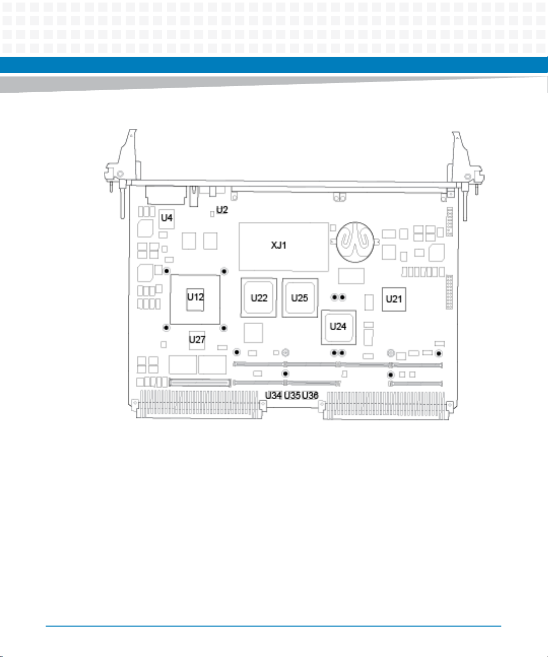
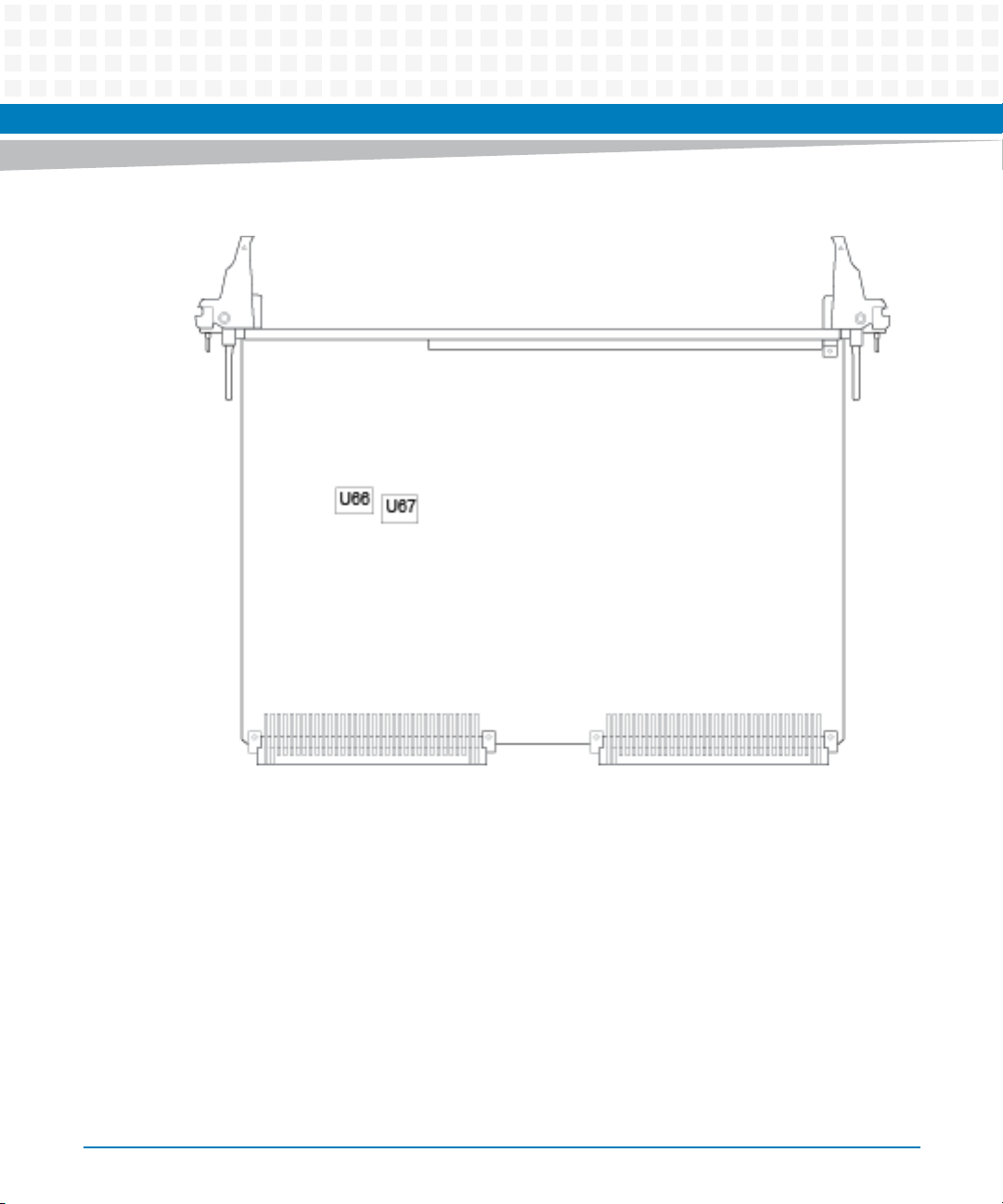
You can find components on the board by their reference designators as shown in Figure 2-1
and Figure 2-2 on the next page. Versions of the board that are not fully populated may not
contain some of these components.
The preferred measurement location for a component may be junction, case, or ambient as
specified in the table. Junction temperature refers to the temperature measured by an on-chip
thermal device. Case temperature refers to the temperature at the top, center surface of the
component. Air temperature refers to the ambient temperature near the component.
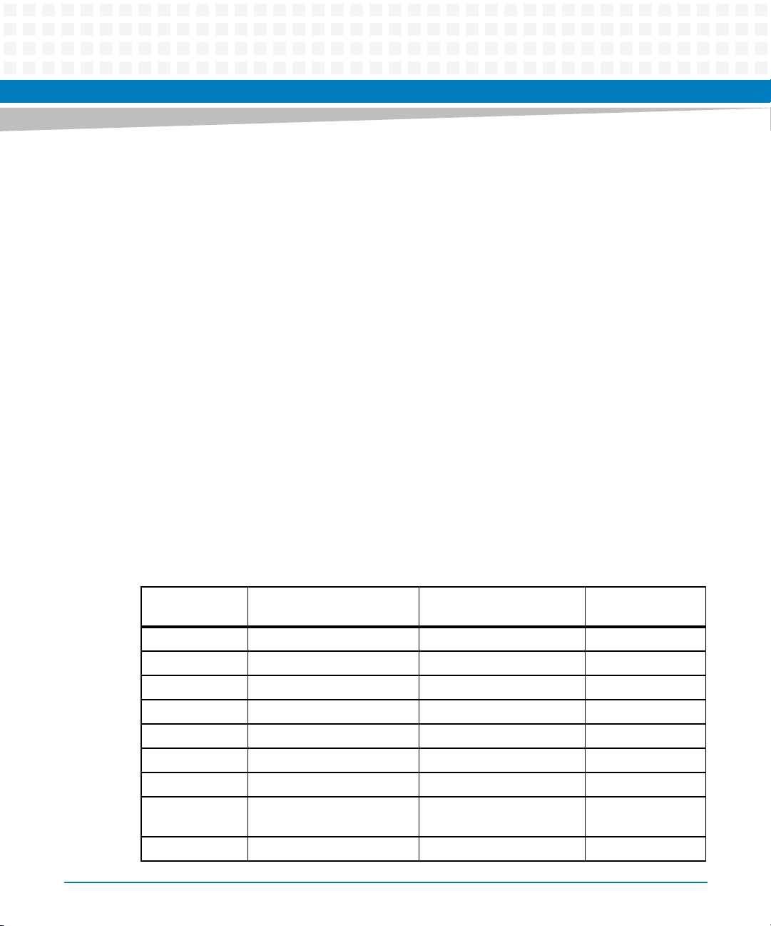
Table 2-4 Thermally Significant Components
Reference
Designator Generic Description
U12 Processor 105 °C (+221 °F) Junction
U4, U27 Gb Ethernet Transceivers 125 °C (+257 °F) Junction
U66 MRAM 115 °C (+239 °F) Junction
U24 VME Bridge 122 °C (+251.6 °F) Junction
U22, U25 PCI-X to PCI-X Bridge 125 °C (+257 °F) Junction
U67 PLD 90 °C (+194 °F) Junction
U21 CPLD 85 °C (+185 °) Junction
U2, U34, U35,
U36
XJ1 DDR2 SDRAM 85 °C (+185 °) Case
Transceivers 150 °C (+302 °F) Junction
Maximum Allowable
Component Temperature
Measurement
Location
MVME4100 Single Board Computer Installation and Use (6806800H18G)
31
Page 32
Hardware Preparation and Installation
Figure 2-1 Primary Side Thermally Significant Components
32
MVME4100 Single Board Computer Installation and Use (6806800H18G)
Page 33
Hardware Preparation and Installation
Figure 2-2 Secondary Side Thermally Significant Components
2.3.5 Equipment Requirements
The following equipment is recommended to complete an MVME4100 system:
VMEbus system enclosure
System console terminal
Operating system (and/or application software)
Transition module and connecting cables
MVME4100 Single Board Computer Installation and Use (6806800H18G)
33
Page 34
Hardware Preparation and Installation
2.4 Configuring the Board
To produce the desired configuration and ensure proper operation of the MVME4100, you may
need to carry out certain hardware modifications before installing the module.
The MVME4100 provides software control over most options: by setting bits in control
registers after installing the module in a system, you can modify its configuration. The
MVME4100 control registers are described in the MVME4100 Programmer’s Reference.
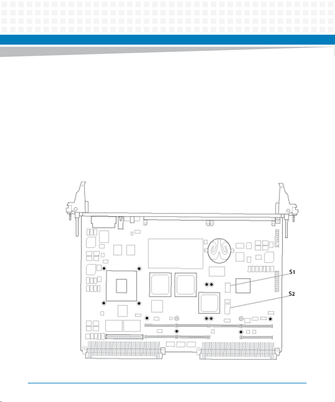
Prior to installing PMC modules on the MVME4100 base board, ensure that all switches that are
user configurable are set properly. To do this, refer to Figure 2-3 or the board itself, for the
location of specific switches and set the switches according to the following descriptions.
Figure 2-3 Switch Locations
34
MVME4100 Single Board Computer Installation and Use (6806800H18G)
Page 35
The following sections describe the on-board switches and their configurations for the
MVME4100.
Board Malfunction
Switches marked as "reserved" might carry production-related functions and can cause the
board to malfunction if their setting is changed.
Do not change settings of switches marked as "reserved". The setting of switches which are
not marked as "reserved" has to be checked and changed before board installation.
2.4.1 SMT Configuration Switch, S1
An 8-position SMT configuration switch is located on the MVME4100 to control the flash bank
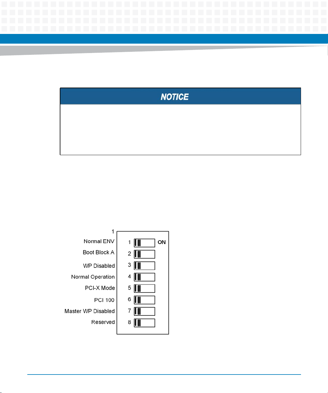
write-protect, select the flash boot image, and control the safe start ENV settings. The default
setting on all switch positions is OFF and is indicated by brackets in Table 2-5.
Hardware Preparation and Installation
Figure 2-4 SMT Configuration Switch Position
MVME4100 Single Board Computer Installation and Use (6806800H18G)
35
Page 36

Hardware Preparation and Installation
Table 2-5 Configuration Switch Settings (S1)
Switch Description Setting Function
S1-1 Safe Start
1
[OFF]
ON
Use normal ENV
Use safe ENV
S1-2 Boot Block B
Select
S1-3 Flash Bank WP [OFF]
S1-4 JTAG Pass Thru [OFF]
S1-5 PCI Mode [OFF]
S1-6 PCI 66 [OFF]
S1-7 MASTER WP [OFF]
S1-8 Reserved - -
[OFF]
ON
ON
ON
ON
ON
ON
Flash memory map normal and boot block A selected
Boot block B selected, mapped to highest address
Entire NOR flash not write-protected
Flash is write-protected
When this switch is on, writes to the NOR flash devices are
blocked by hardware. The FLASH BANK WP switch does
not control writes to the NAND flash.
Normal operation
Pass-Through mode
PCI-X mode
PCI-C, 66 MHz mode
PCI-X 100 MHz mode
PCI 66 mode and PCI bus mode controlled by PCI Mode
switch
Master write-protection (WP) disabled
Master WP on to write protect the NOR flash, NAND flash,
MRAM, and I
This switch does not write protect the SPD on the SO-
CDIMM. Other switches and control bits may writeprotect individual devices.
2
C EEPROM devices
1. Switch status is readable from System Status Register 1, bit 5. Software should check this bit and act accordingly.
2.4.2 Geographical Address Switch, S2
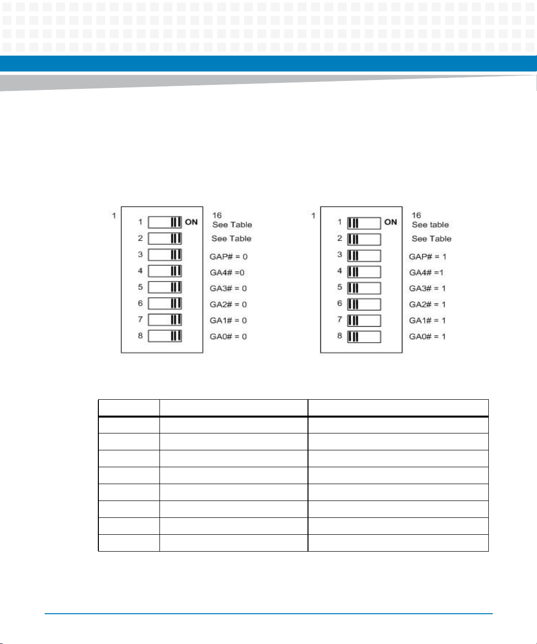
The Tsi148 VMEbus Status Register provides the VMEbus geographical address of the
MVME4100. The switch reflects the inverted states of the geographical address signals.
Applications not using the 5-row backplane can use the geographical address switch to assign
a geographical address per the following diagram. Note that this switch is wired in parallel with
the geographical address pins on the 5-row connector so these switches must be in the off
36
MVME4100 Single Board Computer Installation and Use (6806800H18G)
Page 37
Hardware Preparation and Installation
position when installed in a 5-row chassis in order to get the correct address from the P1
connector. This switch also includes the SCON control switches. More information regarding
GA address switch assignments can be found in the MVME4100 Single Board Computer
Programmer’s Reference.
Figure 2-5 Geographical Address Switch Position
Table 2-6 Geographical Address Switch Settings
Position Function Default
S2-1 VME SCON Auto
S2-2 VME SCON SEL
S2-3 GAP 1
S2-4 GA4 1
S2-5 GA3 1
S2-6 GA2 1
S2-7 GA1 1
S2-8 GA0 1
1. The VME SCON MAN switch is OFF to select Auto-SCON mode. The switch is ON to select manual SCON mode which
works in conjunction with the VME SCON SEL switch.
MVME4100 Single Board Computer Installation and Use (6806800H18G)
1
2
Auto-SCON
Non-SCON
37
Page 38

Hardware Preparation and Installation
2. The VME SCON SEL switch is OFF to select non-SCON mode. The switch is ON to select always SCON mode. This
switch is only effective when the VME SCON MAN switch is ON.
If you are installing the optional MVME7216E transition module, refer to Transition Module on
page 38 for configuration switch settings.
2.5 Installing Accessories
This section describes the procedures for installing the MVME7216E transition module, PMCs,
and the XMCspan on the base board.
2.5.1 Transition Module
The MVME7216E does not support hot swap. You should remove power to the rear slot or
system before installing the module. Before installing the MVME7216E transition module, you
may need to manually configure the switch and install a PMC I/O Module (PIM). Refer to
Chapter 5, Transition Module, for switch settings and PIM installation.
38
Damage of Circuits
Electrostatic discharge and incorrect installation and removal can damage circuits or
shorten their life.
Before touching the board or electronic components, make sure that you are working in an
ESD-safe environment.
Product Damage
Only use injector handles for board insertion to avoid damage to the front panel and/or PCB.
Deformation of the front panel can cause an electrical short or other board malfunction.
Board Malfunction
Switches marked as “reserved” might carry production-related functions and can cause the
board to malfunction if their setting is changed.
Do not change settings of switches marked as “reserved”. The setting of switches which are
not marked as “reserved” has to be checked and changed before board installation.
MVME4100 Single Board Computer Installation and Use (6806800H18G)
Page 39

Hardware Preparation and Installation
Installation and Removal Procedure
To begin the installation of the transition module in a chassis, proceed as follows:
1. Turn all equipment power OFF and disconnect the power cable from the AC power
source.
2. Remove the chassis cover as instructed in the equipment user's manual.
3. Remove the filler panel(s) from the appropriate card slot(s) at the rear of the chassis
(if the chassis has a rear card cage).
4. Install the top and bottom edge of the transition module into the rear guides of the
chassis.
5. Ensure that the levers of the two injector/ejectors are in the outward position.
6. Slide the transition module into the chassis until you feel resistance.
7. Simultaneously move the injector/ejector levers in an inward direction.
8. Verify that the transition module is properly seated and secure it to the chassis
using the two screws located adjacent to the injector/ejector levers.
9. Connect the appropriate cables to the transition module.
To remove the transition module from the chassis, reverse the procedure and press the red
locking tabs (IEEE handles only) to extract the board.
2.5.2 PMC
The PMC connectors are placed to support two single-width PMCs or one double-width PMC.
PMC site 1 supports front PMC I/O and rear PMC I/O via the Jn4 connector. PMC 1 I/O is routed
to the VME P2 connector. PMC site 2 only supports front PMC I/O and does not have a Jn4
connector. The PMC 1 Jn4 user I/O signals only support low-current high-speed signals and thus
do not support current-bearing power supply usage.
MVME4100 Single Board Computer Installation and Use (6806800H18G)
39
Page 40
Hardware Preparation and Installation
The user-configured switches S1 and S2 are not accessible with a PMC installed in PMC site 2.
The onboard PMC sites are configured to support +3.3 V I/O PMC modules. The onboard PMC
sites may be configured to support 3.3V or 5.0V I/O PMC modules. To support 3.3V or 5.0V I/O
PMC modules, both PMC I/O keying pins must be installed in the holes. If both keying pins are
not in the same location or if the keying pins are not installed, the PMC sites will not function.
Note that setting the PMC I/O voltage to 5.0 V forces the PMC sites to operate in 33 MHz PCI
mode instead of PCI-X mode. The default factory configuration is for 3.3 V PMC I/O voltage.
Follow these steps to install a PMC onto the MVME4100 board.
Installation Procedure
Read all notices and follow these steps to install a PMC on the base board.
Damage of Circuits
Electrostatic discharge and incorrect installation and removal can damage circuits or
shorten their life.
Before touching the board or electronic components, make sure that you are working in an
ESD-safe environment.
40
Product Damage
Inserting or removing modules with power applied may result in damage to module
components.
Before installing or removing additional devices or modules, read the documentation that
came with the product.
1. Attach an ESD strap to your wrist.
2. Attach the other end of the ESD strap to the chassis as a ground.
The ESD strap must be secured to your wrist and to ground throughout the
procedure.
3. Remove the PCI filler from the front panel.
MVME4100 Single Board Computer Installation and Use (6806800H18G)
Page 41

Hardware Preparation and Installation
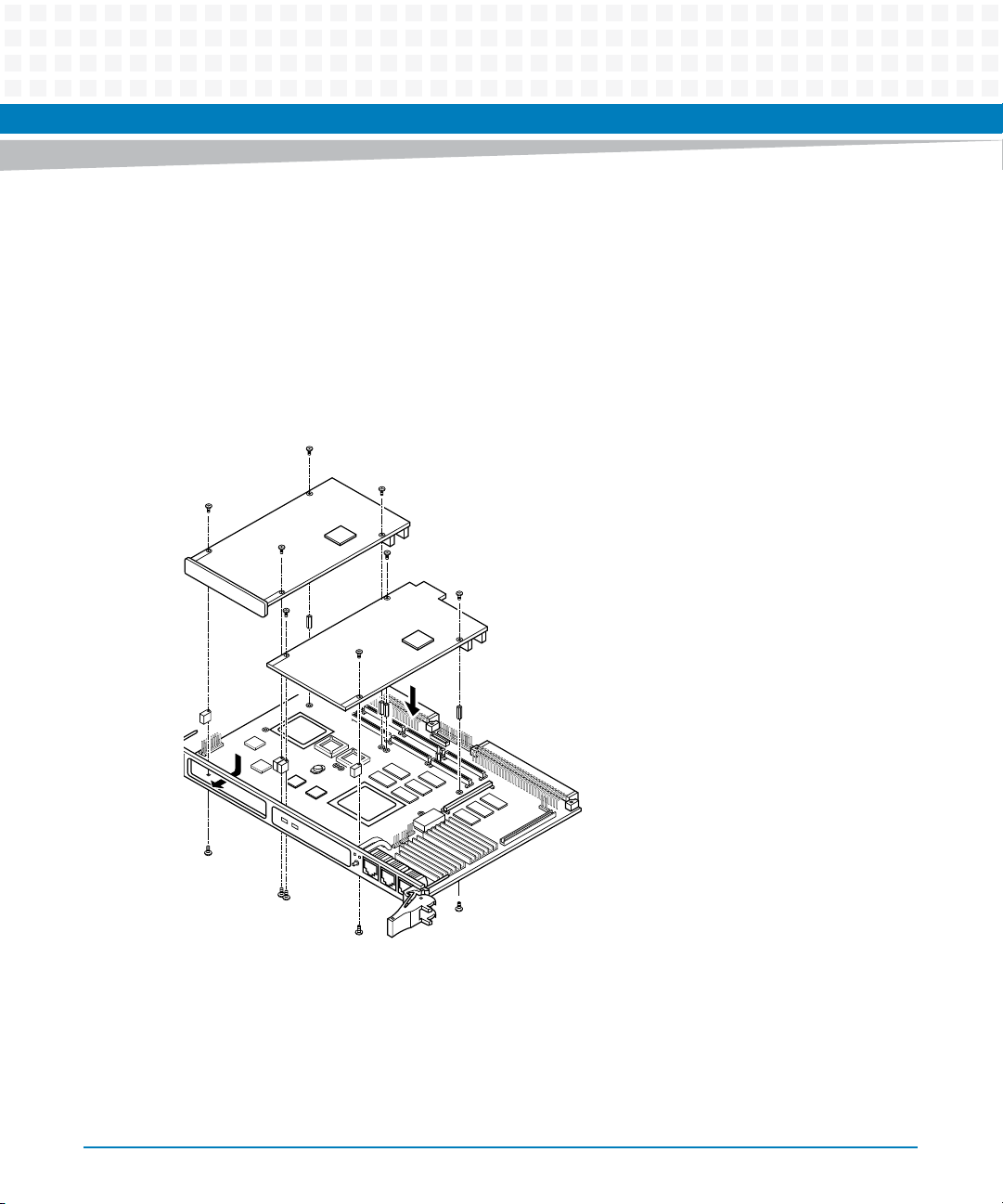
4. Slide the edge connector of the PMC module into the front panel opening from
behind and place the PMC module on top of the base board.
The four connectors on the underside of the PMC module should then connect
smoothly with the corresponding connectors on the MVME4100.
5. Insert the four short phillips-head screws (provided with the PMC) through the
holes on the bottom side of the MVME4100 and the PMC front bezel and into rear
standoffs.
6. Tighten the screws. Refer to Figure 2-6 on page 42.
MVME4100 Single Board Computer Installation and Use (6806800H18G)
41
Page 42
Hardware Preparation and Installation
7. Reinstall the MVME4100 assembly in its proper card slot.
Be sure the module is well seated in the backplane connectors. Do not damage or
bend connector pins.
8. If the PMC module was installed in a non-hot swap chassis, replace the chassis or
system cover(s), reconnect the system to the AC or DC power source and turn the
equipment power on.
Figure 2-6 Typical Placement of a PMC Module on a VME Module
2.5.3 XMCspan
The XMCspan is a carrier module that provides PCI Express expansion capability to the
MVME4100. Refer to the XMCspan Installation and Use manual for details about the XMCspan
and the installation procedure.
42
MVME4100 Single Board Computer Installation and Use (6806800H18G)
Page 43
Hardware Preparation and Installation
2.6 Installing and Removing the Board
This section describes a recommended procedure for installing a board module in a chassis.
The MVME4100 does not support hot swap. You should remove power to the slot or system
before installing the module. Before installing the MVME4100, ensure that the serial ports and
switches are properly configured.
Installation and Removal Procedure
Before you install your module, please read all cautions, warnings and instructions presented
in this section.
Damage of Circuits
Electrostatic discharge and incorrect installation and removal can damage circuits or
shorten their life.
Before touching the board or electronic components, make sure that you are working in an
ESD-safe environment.
Product Damage
Only use injector handles for board insertion to avoid damage to the front panel and/or PCB.
Deformation of the front panel can cause an electrical short or other board malfunction.
Use the following steps to install the MVME4100 into your computer chassis.
1. Attach an ESD strap to your wrist.
2. Attach the other end of the ESD strap to an electrical ground.
The ESD strap must be secured to your wrist and to ground throughout the
procedure.
3. Remove any filler panel that might fill that slot.
4. Install the top and bottom edge of the MVME4100 into the guides of the chassis.
5. Ensure that the levers of the two injector/ejectors are in the outward position.
6. Slide the MVME4100 into the chassis until you feel resistance.
MVME4100 Single Board Computer Installation and Use (6806800H18G)
43
Page 44

Hardware Preparation and Installation
7. Simultaneously move the injector/ejector levers in an inward direction.
8. Verify that the MVME4100 is properly seated.
9. Secure it to the chassis using the two screws located adjacent to the
injector/ejector levers.
10.Connect the appropriate cables to the MVME4100.
To remove the board from the chassis, reverse the procedure and press the red locking tabs
(IEEE handles only) to extract the board.
2.7 Completing the Installation
The MVME4100 is designed to operate as an application-specific compute blade or an
intelligent I/O board/carrier. It can be used in any slot in a VME chassis. When the MVME4100
is installed in a chassis, you are ready to connect peripherals and apply power to the board.
44
Figure 3-1 on page 48 and Figure 5-1 on page 82 show the locations of the various connectors
on the MVME4100 and MVME7216E.
Product Damage
RJ-45 connectors on modules are either twisted-pair Ethernet (TPE) or E1/T1/J1 network
interfaces. Connecting an E1/T1/J1 line to an Ethernet connector may damage your system.
Make sure that TPE connectors near your working area are clearly marked as network
connectors.
Verify that the length of an electric cable connected to a TPE bushing does not exceed
100 m.
Make sure the TPE bushing of the system is connected only to safety extra low voltage
circuits (SELV circuits).
If in doubt, ask your system administrator.
MVME4100 Single Board Computer Installation and Use (6806800H18G)
Page 45

The console settings for the MVME4100 are:
Eight bits per character
One stop bit per character
Parity disabled (no parity)
Baud rate of 9600 baud
Verify that hardware is installed and the power/peripheral cables connected are appropriate for
your system configuration.
Replace the chassis or system cover, reconnect the chassis to the AC or DC power source, and
turn the equipment power on.
2.8 Factory Installed Linux
A bootable ramdisk based Linux image based on the 2.6.27 kernel is available in NOR flash. To
boot this image, use the following MOTLOAD commands:
Hardware Preparation and Installation
MVME4100> bmw -af8000000 -bf8f00000 -c2000000 execP -l2000400
The image should boot to the following prompt:
Emerson Network Power Embedded Computing Linux
Kernel 2.6.27 on a MVME4100 localhost login:
Login as root.
The /root/README.MVME4100_LINUX file provides a brief overview of MVME4100 Linux.
Contact Artesyn Embedded Technologies for kernel patches and additional information on
using MVME4100 Linux.
MVME4100 Single Board Computer Installation and Use (6806800H18G)
45
Page 46

Hardware Preparation and Installation
46
MVME4100 Single Board Computer Installation and Use (6806800H18G)
Page 47

Controls, LEDs, and Connectors
3.1 Overview
This chapter summarizes the controls, LEDs, connectors, and headers for the MVME4100 base
board. Connectors for the MVME7216E transition module can be found in Rear Panel
Connectors on page 85.
Chapter 3
MVME4100 Single Board Computer Installation and Use (6806800H18G)
47
Page 48
Controls, LEDs, and Connectors
3.2 Board Layout
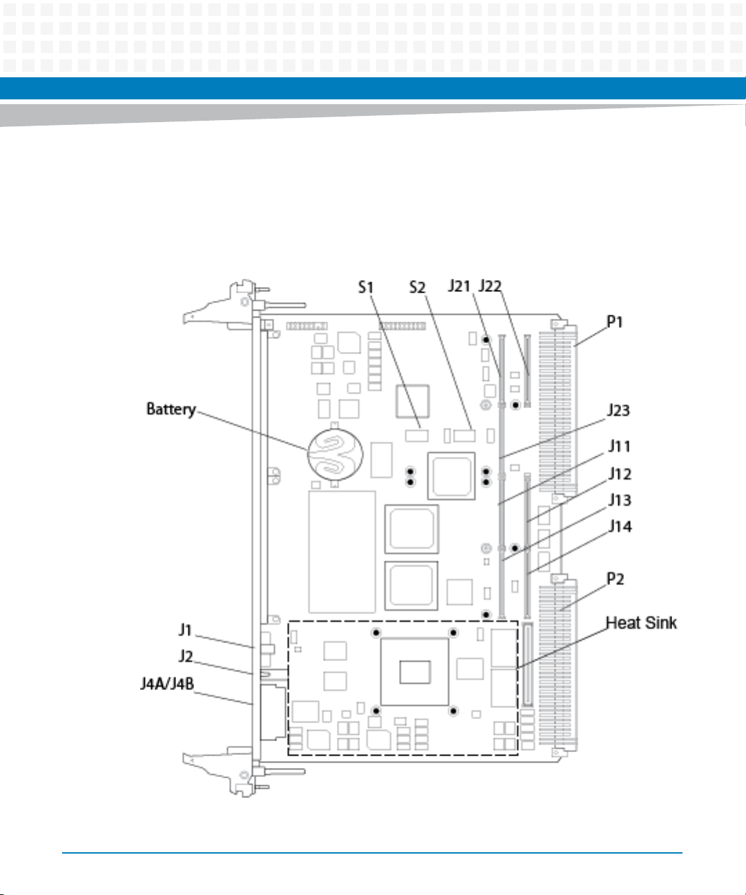
The following figure shows the components, LEDs, connectors, and the reset switch on the
MVME4100.
Figure 3-1 Component Layout
48
MVME4100 Single Board Computer Installation and Use (6806800H18G)
Page 49
3.3 Front Panel
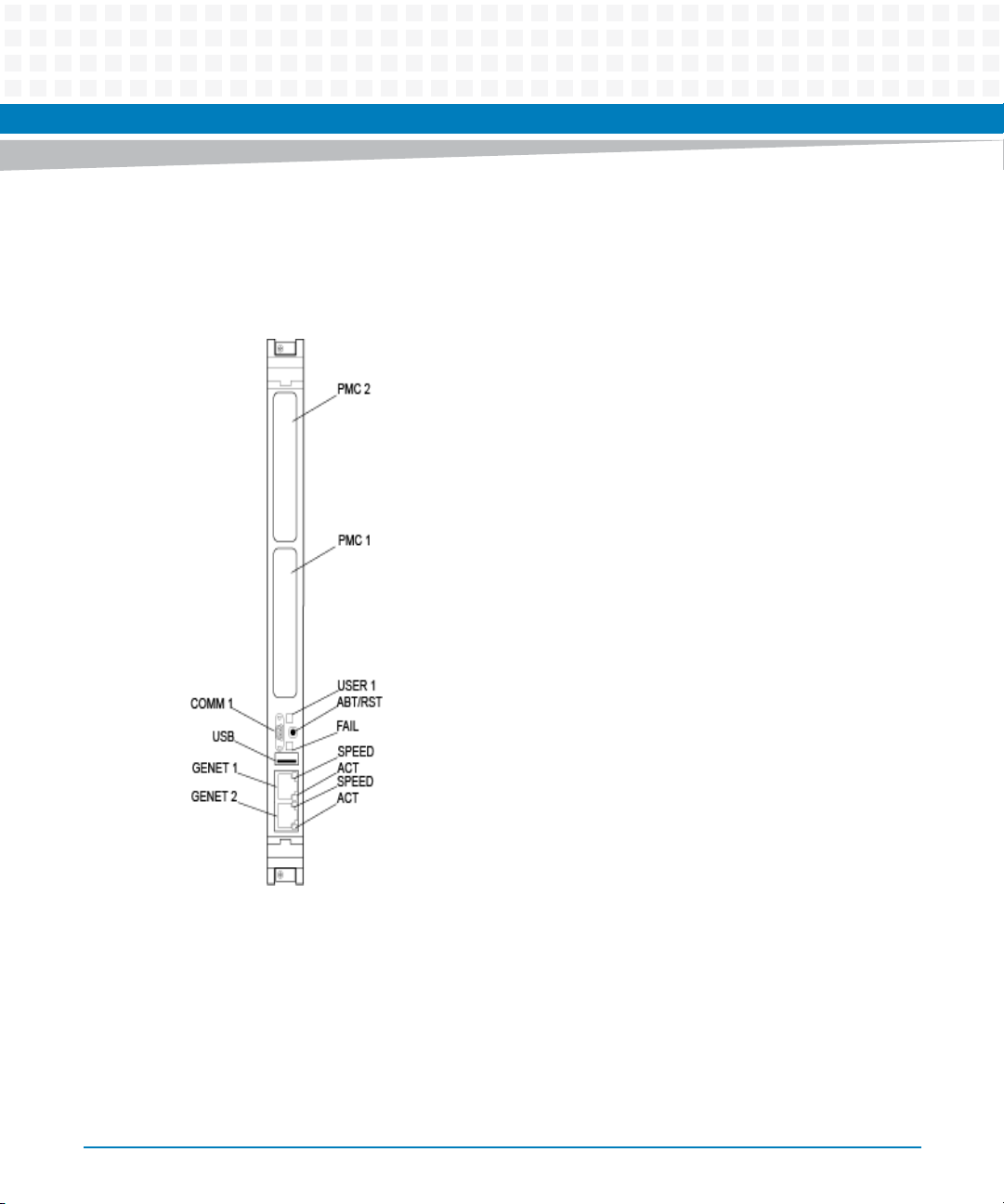
The following switch, LEDs, and connectors are available on the MVME4100 front panel.
Figure 3-2 Front Panel LEDs, Connectors, Switch
Controls, LEDs, and Connectors
3.3.1 Reset/Abort Switch
The MVME4100 has a single push button switch to provide both the abort and reset functions.
When the switch is depressed for less than 3 seconds, an abort interrupt is generated to the
MPC8548E PIC. If the switch is held for more than 3 seconds, a board hard reset is generated. If
the MVME4100 is the VMEbus system controller, a VME SYSRESET is generated.
MVME4100 Single Board Computer Installation and Use (6806800H18G)
49
Page 50

Controls, LEDs, and Connectors
3.3.2 LEDs
The next table describes the LEDs on the front panel of the MVME4100. Refer to Figure 3-2 on
page 49 for LED locations.
Table 3-1 Front Panel LEDs
Label Function Color Description
BFL Board Fail Red This indicator is illuminated during a hard
USR1 User Defined Red/Yellow This indicator is illuminated by S/W
reset and remains illuminated until
software turns it off. The LED is
controlled by bit 14 (BDFAIL) of the
VSTAT register in the Tsi148.
assertion of its corresponding register
bits in the Status Indicator Register. See
the Programmer's Guide for further
details.
50
GNET1 SPEED TSEC1 Link / Speed Off
Yellow
Green
GNET1 ACT TSEC1Activity Off
Blinking Green
GNET2 SPEED TSEC2 Link / Speed Off
Yellow
Green
GNET2 ACT TSEC2 Activity Off
Blinking Green
MVME4100 Single Board Computer Installation and Use (6806800H18G)
No link
10/100 BASE-T operation
1000 BASE-T operation
No activity
Activity proportional to bandwidth
utilization
No link
10/100 BASE-T operation
1000 BASE-T operation
No activity
Activity proportional to bandwidth
utilization
Page 51

3.3.3 Connectors
This section describes the pin assignments and signals for the connectors on the MVME4100.
The next table lists the standard connectors on the MVME4100 base board. Refer to Figure 3-1
on page 48 for connector locations. Pin assignments for the connectors are in the following
sections. Some connectors use standard pin assignments in compliance with the VMEbus, IEEE,
PCI, and ANSI/VITA specifications. Links to these specifications are located at Appendix B,
Related Specifications, on page 122.
Table 3-2 Base Board Connectors
Reference Designator Function Notes
J6 XMC Expansion 8X PCI-E to XMCSpan
J4A TSEC 1, 10/100/1000 Ethernet RJ-45
J4B TSEC 2, 10/100/1000 Ethernet RJ-45
Controls, LEDs, and Connectors
GENET 1 on front
GENET2 on front
J11, J12, J13, J14
J21, J22, J23
J1 Port 0. Serial Port 1 Micro DB-9 console serial port on front
P1 VME five-row P1
P2 VME five-row P2 on SBC and RTM TSEC3 signals assigned to E1-1 thru E1-4
J2 USB Single channel upright USB connector.
P4 Processor COP header Planar header for processor COP
P5 Boundary Scan header Planar header for boundary scan and
MVME4100 Single Board Computer Installation and Use (6806800H18G)
PMC1
PMC2
Implementing all recommended and
optional VITA32 signals except
RESETOUT#
TSEC4 signals assigned to E2-1 thru E2-4
Serial ports 2-5
USB1 on front
USB2 on RTM
emulation
PLD/flash programming
51
Page 52
Controls, LEDs, and Connectors
3.3.3.1 XMC Expansion Connector (J6)
One 76-pin Mictor connector with a center row of ground pins is used to provide XMC
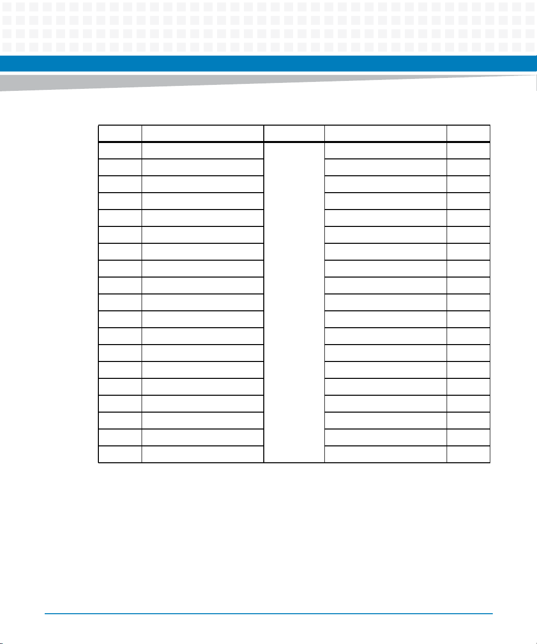
expansion capability. The pin assignments for this connector are as follows:
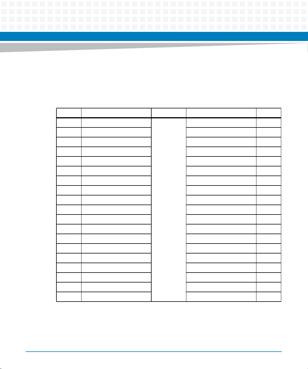
Table 3-3 XMC Expansion Connector (J6) Pin Assignments
Pin Signal Signal Pin
1 GND GND GND 2
3 TX0_P RX0_P 4
5 TX0_N RX0_N 6
7GND GND 8
9 TX1_P RX1_P 10
11 TX1_N RX1_N 12
13 GND GND 14
15 TX2_P RX2_P 16
17 TX2_N RX2_N 18
19 GND GND 20
21 TX3_P RX3_P 22
23 TX3_N RX3_N 24
25 GND GND 26
27 REFCLK_P No Connect 28
29 REFCLK_N No Connect 30
31 GND GND 32
33 No Connect No Connect 34
35 No Connect PCIE_END_N 36
37 INT_N RESET_N 38
52
MVME4100 Single Board Computer Installation and Use (6806800H18G)
Page 53
Controls, LEDs, and Connectors
Table 3-3 XMC Expansion Connector (J6) Pin Assignments (continued)
Pin Signal Signal Pin
39 GND GND GND 40
41 TX4_P RX4_P 42
43 TX4_N RX4_N 44
45 GND GND 46
47 TX5_P RX5_P 48
49 TX5_N RX5_N 50
51 GND GND 52
53 TX6_P RX6_P 54
55 TX6_N RX6_N 56
57 GND GND 58
59 TX7_P RX7_P 60
61 TX7_N RX7_N 62
63 GND GND 64
65 No Connect No Connect 66
67 No Connect No Connect 68
69 TDI TDO 70
71 TRST_N I2C_CLK 72
73 TMS I2C_DATA 74
75 TCK PRESENT_N 76
MVME4100 Single Board Computer Installation and Use (6806800H18G)
53
Page 54
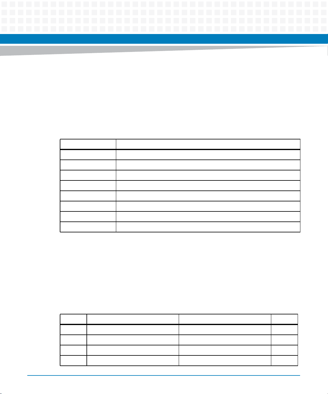
Controls, LEDs, and Connectors
3.3.3.2 Ethernet Connectors (J4A/J4B)
There are four 10/100/1000 Mb/s full duplex Ethernet interfaces using the MPC8548E Triple
Speed Ethernet Controllers (TSECs). Two Gigabit Ethernet interfaces are routed to the two
front-panel RJ-45 connectors with integrated LEDs for speed and activity indication. The other
Gigabit Ethernet interfaces are routed to P2 for rear I/O. These connectors use standard pin
assignments and are as follows:
Table 3-4 Ethernet Connectors (J4A/J4B) Pin Assignments
Pin # 10/100/1000 Mb/s
1_DA+
2_DA-
3 _DB+
4 _DC+
5 _DC-
6 _DB-
7 _DD+
8 _DD-
3.3.3.3 PCI Mezzanine Card (PMC) Connectors (J11 – J14, J21 – J23)
There are seven 64-pin SMT connectors on the MVME4100 to provide 32/64-bit PCI interfaces
and P2 I/O for one optional add-on PMC.
PMC slot connector J14 contains the signals that go to VME P2 I/O rows A, C, D, and Z. The pin
assignments for these connectors are as follows:
Table 3-5 PMC Slot 1 Connector (J11) Pin Assignments
Pin Signal Signal Pin
1 TCK -12V 2
3GND INTA# 4
5 INTB# INTC# 6
7 PMCPRSNT1# +5V 8
54
MVME4100 Single Board Computer Installation and Use (6806800H18G)
Page 55

Controls, LEDs, and Connectors
Table 3-5 PMC Slot 1 Connector (J11) Pin Assignments (continued)
Pin Signal Signal Pin
9 INTD# PCI_RSVD (No Connect) 10
11 GND +3.3Vaux (No Connect) 12
13 CLK GND 14
15 GND PMCGNT1# 16
17 PMCREQ1# +5V 18
19 +3.3V (VIO) AD31 20
21 AD28 AD27 22
23 AD25 GND 24
25 GND C/BE3# 26
27 AD22 AD21 28
29 AD19 +5V 30
31 +3.3V (VIO) AD17 32
33 FRAME# GND 34
35 GND IRDY# 36
37 DEVSEL# +5V 38
39 PCIXCAP LOCK# 40
41 PCI_RSVD (No Connect) PCI_RSVD (No Connect) 42
43 PAR GND 44
45 +3.3V (VIO) AD15 46
47 AD12 AD11 48
49 AD09 +5V 50
51 GND C/BE0# 52
53 AD06 AD05 54
55 AD04 GND 56
57 +3.3V (VIO) AD03 58
59 AD02 AD01 60
61 AD00 +5V 62
MVME4100 Single Board Computer Installation and Use (6806800H18G)
55
Page 56
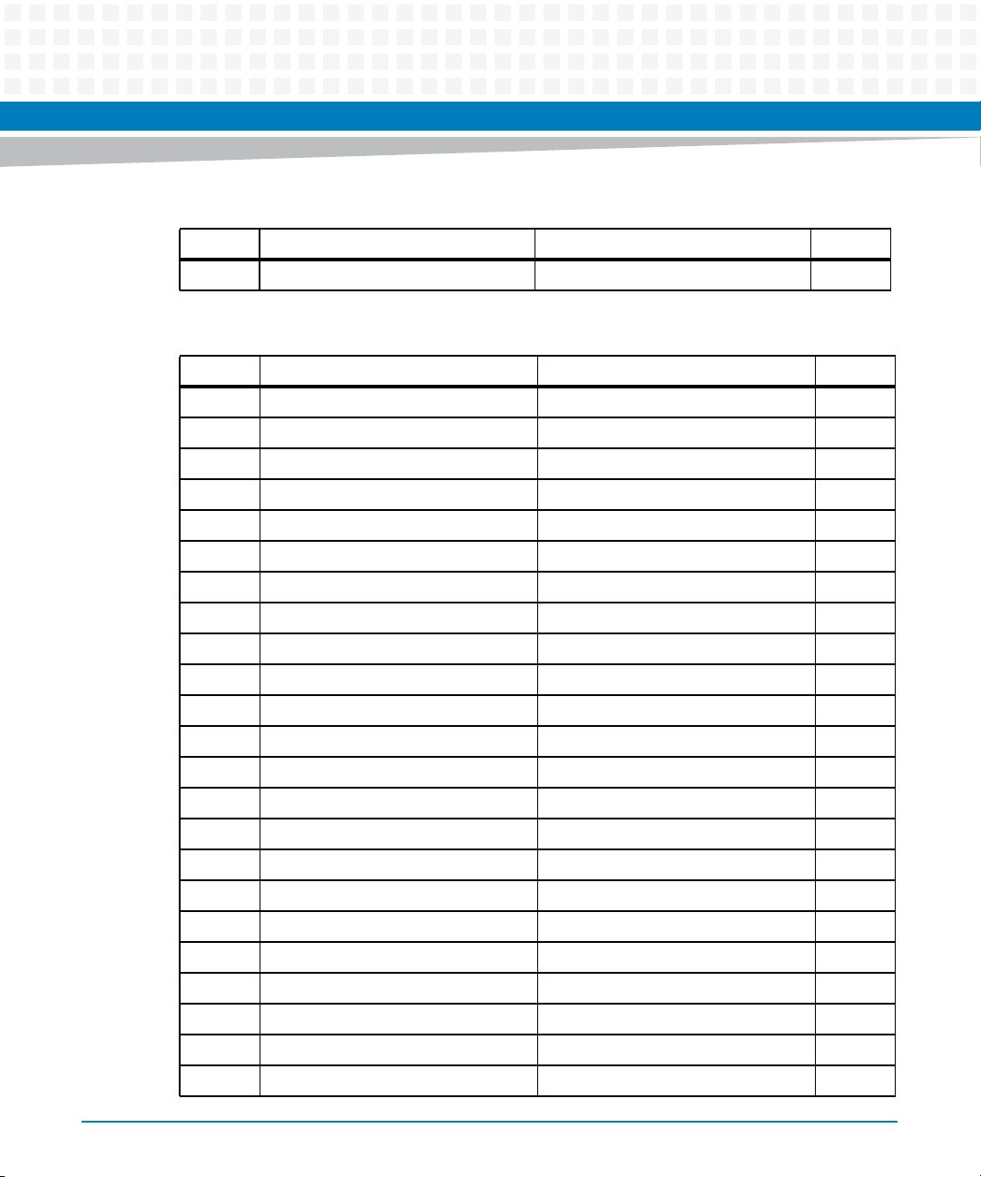
Controls, LEDs, and Connectors
Table 3-5 PMC Slot 1 Connector (J11) Pin Assignments (continued)
Pin Signal Signal Pin
63 GND REQ64# 64
Table 3-6 PMC Slot 1 Connector (J12) Pin Assignments
Pin Signal Signal Pin
1 +12V TRST# 2
3 TMS TDO 4
5 TDI GND 6
7 GND Not Used 8
9 Not Used Not Used 10
11 Pull-up to +3.3V +3.3V 12
13 RST# Pull-down 14
15 +3.3V Pull-down 16
17 Not Used GND 18
19 AD30 AD29 20
21 GND AD26 22
23 AD24 +3.3V 24
25 IDSEL1 AD23 26
27 +3.3V AD20 28
29 AD18 GND 30
31 AD16 C/BE2# 32
33 GND IDSEL1B 34
35 TRDY# +3.3V 36
37 GND STOP# 38
39 PERR# GND 40
41 +3.3V SERR# 42
43 C/BE1# GND 44
45 AD14 AD13 46
56
MVME4100 Single Board Computer Installation and Use (6806800H18G)
Page 57
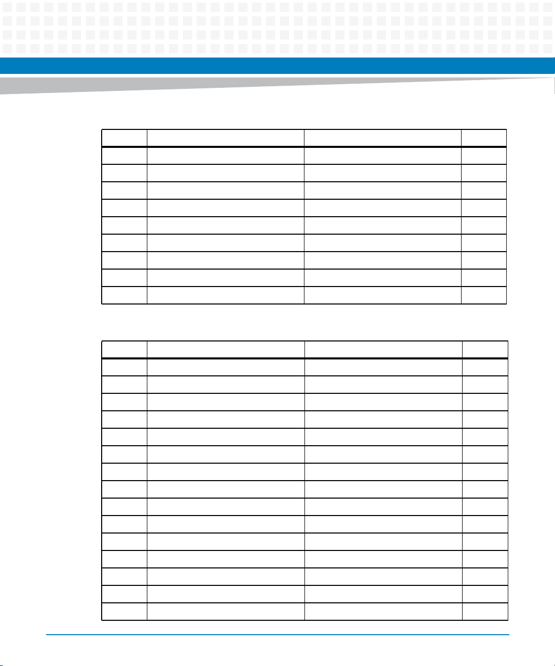
Controls, LEDs, and Connectors
Table 3-6 PMC Slot 1 Connector (J12) Pin Assignments (continued)
Pin Signal Signal Pin
47 M66EN AD10 48
49 AD08 +3.3V 50
51 AD07 REQ1B# 52
53 +3.3V GNT1B# 54
55 Not Used GND 56
57 Not Used EREADY0 58
59 GND Not Used 60
61 ACK64# +3.3V 62
63 GND No Connect (MONARCH#) 64
Table 3-7 PMC Slot 1 Connector (J13) Pin Assignments
Pin Signal Signal Pin
1 Reserved (No Connect) GND 2
3 GND C/BE7# 4
5 C/BE6# C/BE5# 6
7 C/BE4# GND 8
9 +3.3V (VIO) PAR64 10
11 AD63 AD62 12
13 AD61 GND 14
15 GND AD60 16
17 AD59 AD58 18
19 AD57 GND 20
21 +3.3V (VIO) AD56 22
23 AD55 AD54 24
25 AD53 GND 26
27 GND AD52 28
29 AD51 AD50 30
MVME4100 Single Board Computer Installation and Use (6806800H18G)
57
Page 58
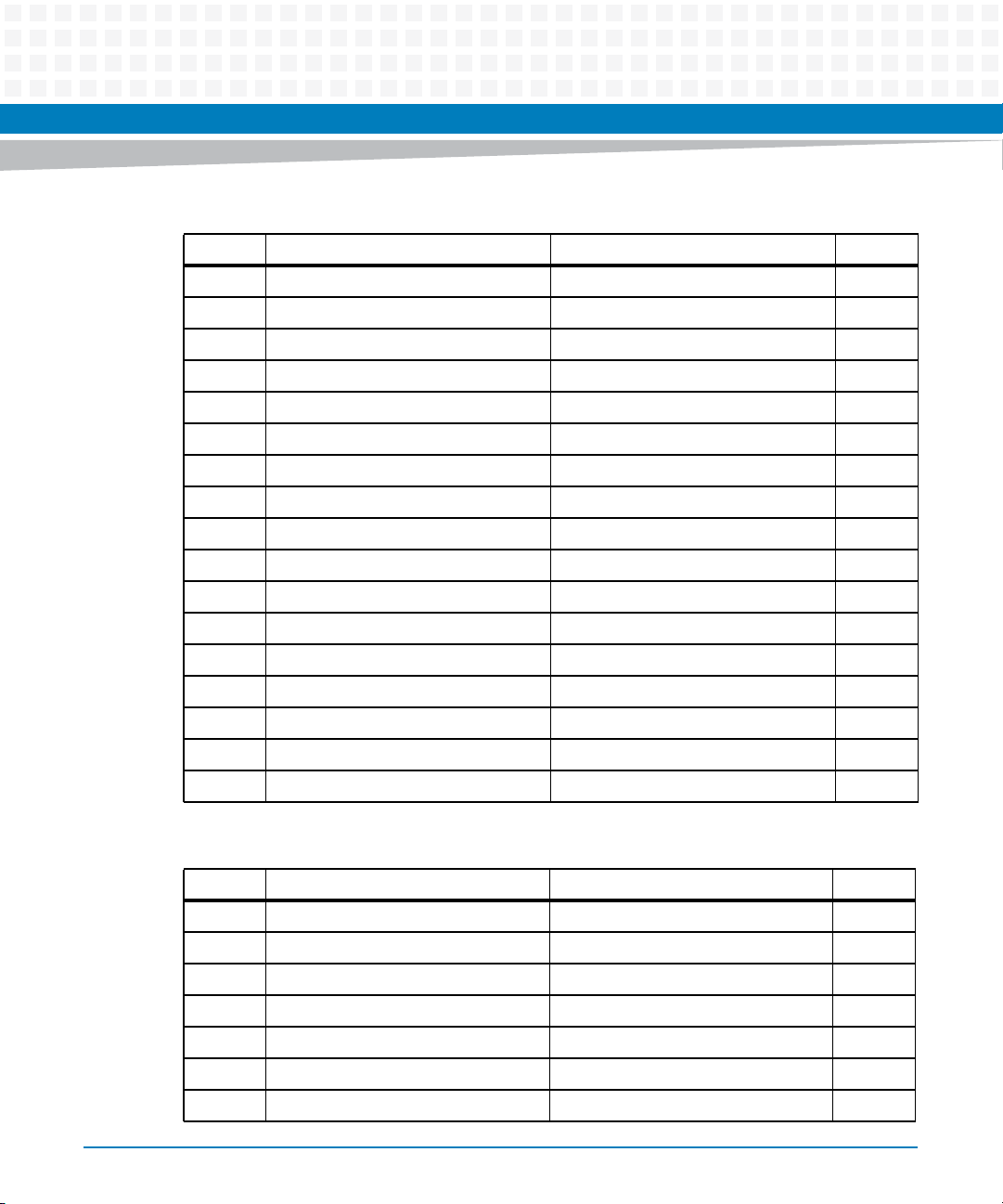
Controls, LEDs, and Connectors
Table 3-7 PMC Slot 1 Connector (J13) Pin Assignments (continued)
Pin Signal Signal Pin
31 AD49 GND 32
33 GND AD48 34
35 AD47 AD46 36
37 AD45 GND 38
39 +3.3V (VIO) AD44 40
41 AD43 AD42 42
43 AD41 GND 44
45 GND AD40 46
47 AD39 AD38 48
49 AD37 GND 50
51 GND AD36 52
58
53 AD35 AD34 54
55 AD33 GND 56
57 +3.3V (VIO) AD32 58
59 Reserved (No Connect) Reserved (No Connect) 60
61 Reserved (No Connect) GND 62
63 GND Reserved (No Connect) 64
Table 3-8 PMC Slot 1 Connector (J14) Pin Assignments
Pin Signal Signal Pin
1 PMC1_1 (P2-C1) PMC1_2 (P2-A1) 2
3 PMC1_3 (P2-C2) PMC1_4 (P2-A2) 4
5 PMC1_5 (P2-C3) PMC1_6 (P2-A3) 6
7 PMC1_7 (P2-C4) PMC1_8 (P2-A4) 8
9 PMC1 _9 (P2-C5) PMC1_10 (P2-A5) 10
11 PMC1_11 (P2-C6) PMC1_12 (P2-A6) 12
13 PMC1_13 (P2-C7) PMC1_14 (P2-A7) 14
MVME4100 Single Board Computer Installation and Use (6806800H18G)
Page 59

Controls, LEDs, and Connectors
Table 3-8 PMC Slot 1 Connector (J14) Pin Assignments (continued)
Pin Signal Signal Pin
15 PMC1_15 (P2-C8) PMC1_16 (P2-A8) 16
17 PMC1_17 (P2-C9) PMC1_18 (P2-A9) 18
19 PMC1_19 (P2-C10) PMC1_20 (P2-A10) 20
21 PMC1PMC1_21 (P2-C11) PMC1_22 (P2-A11) 22
23 PMC1_23 (P2-C12) PMC1_24 (P2-A12) 24
25 PMC1_25 (P2-C13) PMC1_26 (P2-A13) 26
27 PMC1_27 (P2-C14) PMC1_28 (P2-A14) 28
29 PMC1_29 (P2-C15) PMC1_30 (P2-A15) 30
31 PMC1_31 (P2-C16) PMC1_32 (P2-A16) 32
33 PMC1_33 (P2-C17) PMC1_34 (P2-A17) 34
35 PMC1_35 (P2-C18) PMC1_36 (P2-A18) 36
37 PMC1_37 (P2-C19) PMC1_38 (P2-A19) 38
39 PMC1_39 (P2-C20) PMC1_40 (P2-A20) 40
41 PMC1_41 (P2-C21) PMC1_42 (P2-A21) 42
43 PMC1_43 (P2-C22) PMC1_44 (P2-A22) 44
45 PMC1_45 (P2-C23) PMC1_46 (P2-A23) 46
47 PMC1_47 (P2-C24) PMC1_48 (P2-A24) 48
49 PMC1_49 (P2-C25) PMC1_50 (P2-A25) 50
51 PMC1_51 (P2-C26) PMC1_52 (P2-A26) 52
53 PMC1_53 (P2-C27) PMC1_54 (P2-A27) 54
55 PMC1_55 (P2-C28) PMC1_56 (P2-A28) 56
57 PMC1_57 (P2-C29) PMC1_58 (P2-A29) 58
59 PMC1_59 (P2-C30) PMC1_60 (P2-A30) 60
61 PMC1_61 (P2-C31) PMC1_62 (P2-A31) 62
63 PMC1_63 (P2-C32) PMC1_64 (P2-A32) 64
MVME4100 Single Board Computer Installation and Use (6806800H18G)
59
Page 60

Controls, LEDs, and Connectors
Table 3-9 PMC Slot 2 Connector (J21) Pin Assignments
Pin Signal Signal Pin
1 TCK -12V 2
3GND INTC# 4
5 INTD# INTA# 6
7 PMCPRSNT1# +5V 8
9 INTB# PCI_RSVD (No Connect) 10
11 GND +3.3Vaux (No Connect) 12
13 CLK GND 14
15 GND PMCGNT1# 16
17 PMCREQ1# +5V 18
19 +3.3V (VIO) AD31 20
21 AD28 AD27 22
60
23 AD25 GND 24
25 GND C/BE3# 26
27 AD22 AD21 28
29 AD19 +5V 30
31 +3.3V (VIO) AD17 32
33 FRAME# GND 34
35 GND IRDY# 36
37 DEVSEL# +5V 38
39 PCIXCAP LOCK# 40
41 PCI_RSVD (No Connect) PCI_RSVD (No Connect) 42
43 PAR GND 44
45 +3.3V (VIO) AD15 46
47 AD12 AD11 48
49 AD09 +5V 50
51 GND C/BE0# 52
53 AD06 AD05 54
MVME4100 Single Board Computer Installation and Use (6806800H18G)
Page 61
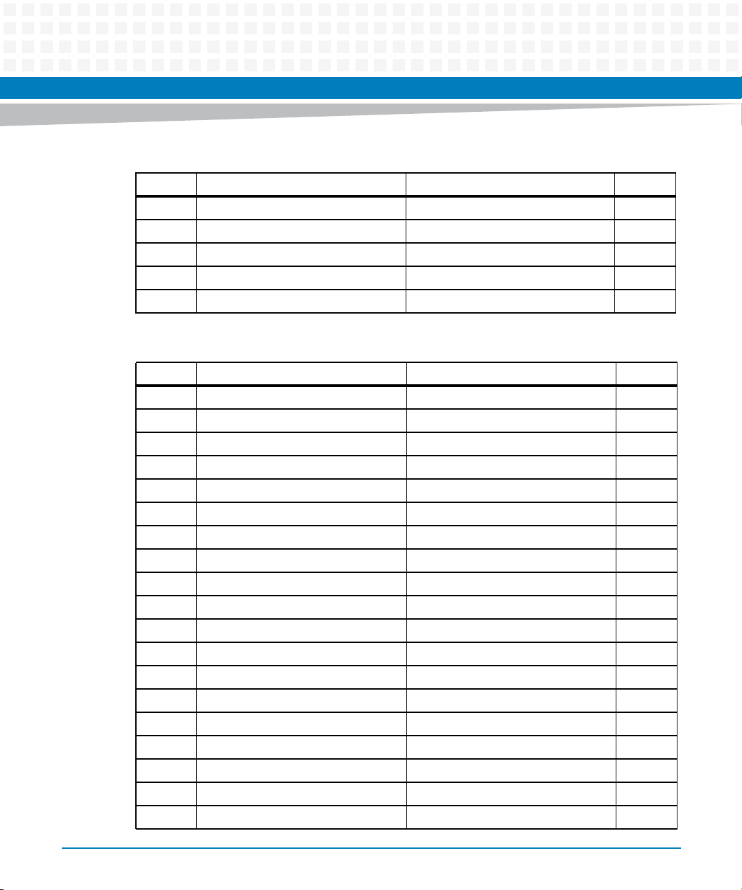
Controls, LEDs, and Connectors
Table 3-9 PMC Slot 2 Connector (J21) Pin Assignments (continued)
Pin Signal Signal Pin
55 AD04 GND 56
57 +3.3V (VIO) AD03 58
59 AD02 AD01 60
61 AD00 +5V 62
63 GND REQ64# 64
Table 3-10 PMC Slot 2 Connector (J22) Pin Assignments
Pin Signal Signal Pin
1 +12V TRST# 2
3 TMS TDO 4
5 TDI GND 6
7 GND Not Used 8
9 Not Used Not Used 10
11 Pull-up to +3.3V +3.3V 12
13 RST# Pull-down 14
15 +3.3V Pull-down 16
17 Not Used GND 18
19 AD30 AD29 20
21 GND AD26 22
23 AD24 +3.3V 24
25 IDSEL1 AD23 26
27 +3.3V AD20 28
29 AD18 GND 30
31 AD16 C/BE2# 32
33 GND IDSEL1B 34
35 TRDY# +3.3V 36
37 GND STOP# 38
MVME4100 Single Board Computer Installation and Use (6806800H18G)
61
Page 62
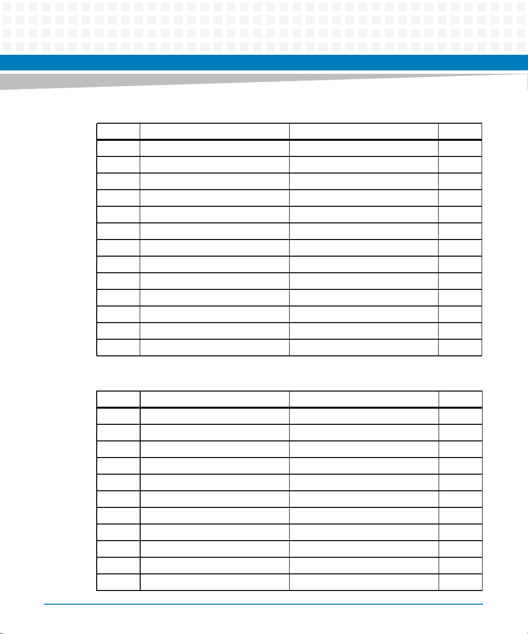
Controls, LEDs, and Connectors
Table 3-10 PMC Slot 2 Connector (J22) Pin Assignments (continued)
Pin Signal Signal Pin
39 PERR# GND 40
41 +3.3V SERR# 42
43 C/BE1# GND 44
45 AD14 AD13 46
47 M66EN AD10 48
49 AD08 +3.3V 50
51 AD07 REQ1B# 52
53 +3.3V GNT1B# 54
55 Not Used GND 56
57 Not Used EREADY1 58
59 GND RSTOUT# 60
62
61 ACK64# +3.3V 62
63 GND No Connect (MONARCH#) 64
Table 3-11 PMC Slot 2 Connector (J23) Pin Assignments
Pin Signal Signal Pin
1 Reserved (No Connect) GND 2
3 GND C/BE7# 4
5 C/BE6# C/BE5# 6
7 C/BE4# GND 8
9 +3.3V (VIO) PAR64 10
11 AD63 AD62 12
13 AD61 GND 14
15 GND AD60 16
17 AD59 AD58 18
19 AD57 GND 20
21 +3.3V (VIO) AD56 22
MVME4100 Single Board Computer Installation and Use (6806800H18G)
Page 63

Controls, LEDs, and Connectors
Table 3-11 PMC Slot 2 Connector (J23) Pin Assignments (continued)
Pin Signal Signal Pin
23 AD55 AD54 24
25 AD53 GND 26
27 GND AD52 28
29 AD51 AD50 30
31 AD49 GND 32
33 GND AD48 34
35 AD47 AD46 36
37 AD45 GND 38
39 +3.3V (VIO) AD44 40
41 AD43 AD42 42
43 AD41 GND 44
45 GND AD40 46
47 AD39 AD38 48
49 AD37 GND 50
51 GND AD36 52
53 AD35 AD34 54
55 AD33 GND 56
57 +3.3V (VIO) AD32 58
59 Reserved (No Connect) Reserved (No Connect) 60
61 Reserved (No Connect) GND 62
63 GND Reserved (No Connect) 64
MVME4100 Single Board Computer Installation and Use (6806800H18G)
63
Page 64
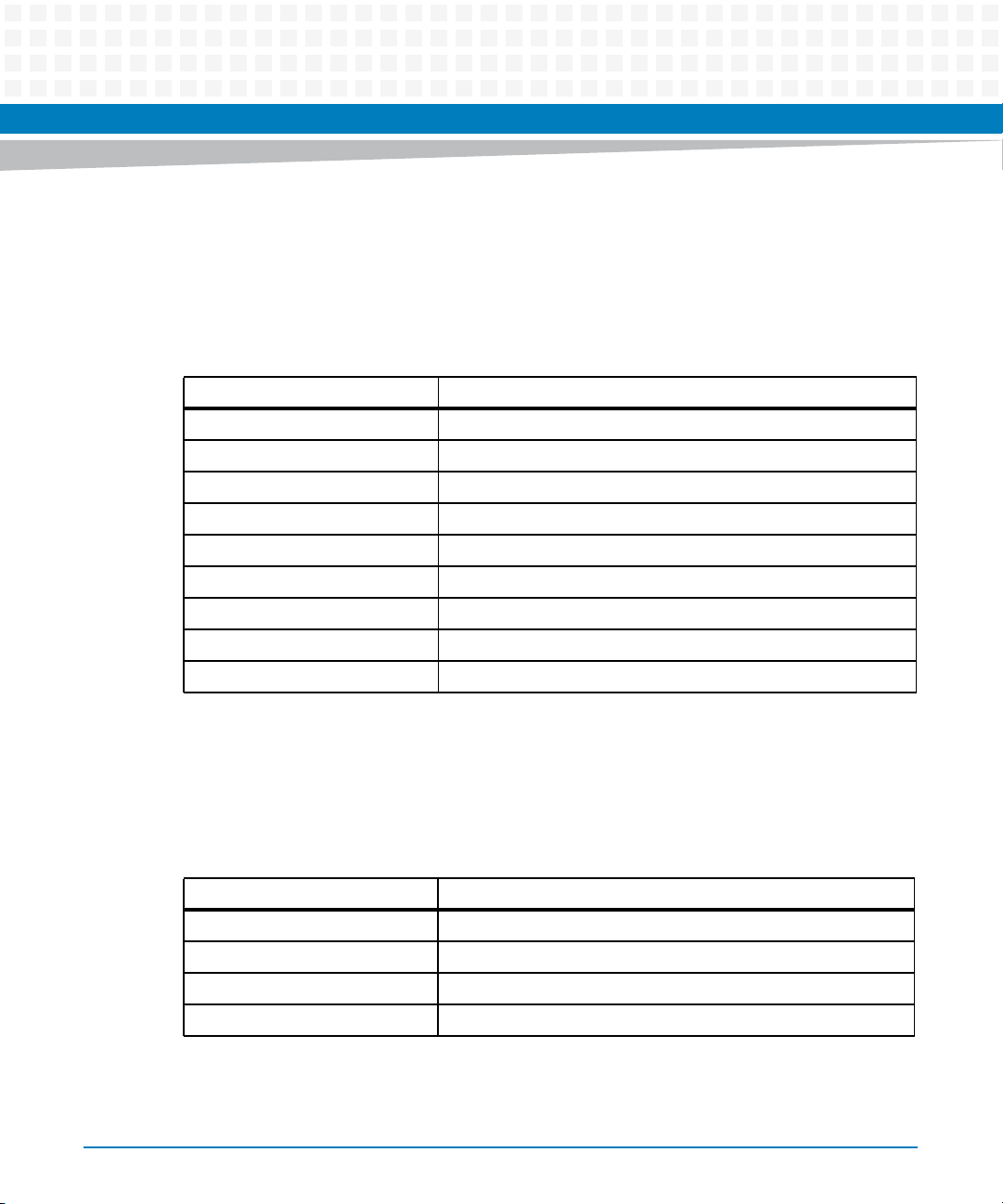
Controls, LEDs, and Connectors
3.3.3.4 Serial Port Connector (COM1/J1)
There is one front access asynchronous serial port interface (SP0) that is routed to the micro
DB-9 front-panel connector. You can use the Artesyn part SERIAL-MINI-D2 to convert to a DB9
male connector. The pin assignments for this connector are as follows:
Table 3-12 COM1 Port Connector Pin Assignments
Pin Signal
1 No Connect
2RX
3TX
4 No Connect
5GND
6 No Connect
7RTS
8CTS
9 No Connect
3.3.3.5 USB Connector (J2)
There is one USB Type A connector located on the MVME4100 front panel. The pin assignments
are as follows:
Table 3-13 USB Connector (J2) Pin Assignments
Pin Signal
1 USB_VBUS (+5.0V)
2 USB_DATA-
3 USB_DATA+
4GND
64
MVME4100 Single Board Computer Installation and Use (6806800H18G)
Page 65
3.3.3.6 VMEbus P1 Connector
The VME P1 connector is a 160-pin DIN. The P1 connector provides power and VME signals for
24-bit address and 16-bit data. The pin assignments for the P1 connector is as follows:
Table 3-14 VMEbus P1 Connector Pin Assignments
Pin ROW Z ROW A ROW B ROW C ROW D Pin
1 Reserved (N/C) D00 BBSY* D08 +5V 1
2 GND D01 BCLR* D09 GND 2
3 Reserved (N/C) D02 ACFAIL* D10 Reserved (N/C) 3
4 GND D03 BG0IN* D11 Reserved (N/C) 4
5 Reserved (N/C) D04 BG0OUT* D12 Reserved (N/C) 5
6 GND D05 BG1IN* D13 Reserved (N/C) 6
7 Reserved (N/C) D06 BG1OUT* D14 Reserved (N/C) 7
Controls, LEDs, and Connectors
8 GND D07 BG2IN* D15 Reserved (N/C) 8
9 Reserved (N/C) GND BG2OUT* GND GAP_L 9
10 GND SYSCLK BG3IN* SYSFAIL* GA0_L 10
11 Reserved (N/C) GND BG3OUT* BERR* GA1_L 11
12 GND DS1* BR0* SYSRESET* +3.3V (Not Used) 12
13 Reserved (N/C) DS0* BR1* LWORD* GA2_L 13
14 GND WRITE* BR2* AM5 +3.3V (Not Used) 14
15 Reserved (N/C) GND BR3* A23 GA3_L 15
16 GND DTACK* AM0 A22 +3.3V (Not Used) 16
17 Reserved (N/C) GND AM1 A21 GA4_L 17
18 GND AS* AM2 A20 +3.3V (Not Used) 18
19 Reserved (N/C) GND AM3 A19 Reserved (N/C) 19
20 GND IACK* GND A18 +3.3V (Not Used) 20
21 Reserved (N/C) IACKIN* SERA (N/C) A17 Reserved (N/C) 21
22 GND IACKOUT* SERB (N/C) A16 +3.3V (Not Used) 22
23 Reserved (N/C) AM4 GND A15 Reserved (N/C) 23
MVME4100 Single Board Computer Installation and Use (6806800H18G)
65
Page 66
Controls, LEDs, and Connectors
Table 3-14 VMEbus P1 Connector Pin Assignments (continued)
Pin ROW Z ROW A ROW B ROW C ROW D Pin
24 GND A07 IRQ7* A14 +3.3V (Not Used) 24
25 Reserved (N/C) A06 IRQ6* A13 Reserved (N/C) 25
26 GND A05 IRQ5* A12 +3.3V (Not Used) 26
27 Reserved (N/C) A04 IRQ4* A11 Reserved (N/C) 27
28 GND A03 IRQ3* A10 +3.3V (Not Used) 28
29 Reserved (N/C) A02 IRQ2* A09 Reserved (N/C) 29
30 GND A01 IRQ1* A08 +3.3V (Not Used) 30
31 Reserved (N/C) -12V +5VSTDBY
32 GND +5V +5V +5V +5V 32
3.3.3.7 VMEbus P2 Connector
The VME P2 connector is a 160-pin DIN. Row B of the P2 connector provides power to the
MVME4100 and to the upper eight VMEbus address lines and additional 16 VMEbus data lines.
The Z, A, C, and D pin assignments for the P2 connector are the same for both the MVME4100
and MVME7216E, and are as follows:
Table 3-15 VME P2 Connector Pinouts
Pin P2-Z P2-A P2-B P2-C P2-D
1 SP1RX PMC1_IO2 +5V PMC1_IO1 E1-1+
2 GND PMC1_IO4 GND PMC1_IO3 E1-1-
3 SPITX PMC1_IO6 VRETRY_L PMC1_IO5 GND
4 GND PMC1_IO8 VA24 PMC1_IO7 E1-2+
5 SP1CTS PMC1_IO10 VA25 PMC1_IO9 E1-2-
6 GND PMC1_IO12 VA26 PMC1_IO11 GND
+12V GND 31
(N/C)
66
7 SP1RTS PMC1_IO14 VA27 PMC1_IO13 E1-3+
8 GND PMC1_IO16 VA28 PMC1_IO15 E1-3-
9 SP2RX PMC1_IO18 VA29 PMC1_IO17 GND
MVME4100 Single Board Computer Installation and Use (6806800H18G)
Page 67
Controls, LEDs, and Connectors
Table 3-15 VME P2 Connector Pinouts (continued)
Pin P2-Z P2-A P2-B P2-C P2-D
10 GND PMC1_IO20 VA30 PMC1_IO19 E1-4+
11 SP2TX PMC1_IO22 VA31 PMC1_IO21 E1-4-
12 GND PMC1_IO24 GND PMC1_IO23 GND
13 SP2CTS PMC1_IO26 +5V PMC1_IO25 I2C_SDA
14 GND PMC1_IO28 VD16 PMC1_IO27 I2C_SCL
15 SP2RTS PMC1_IO30 VD17 PMC1_IO29 E1_LINK
16 GND PMC1_IO32 VD18 PMC1_IO31 E1_ACT
17 SP3RX PMC1_IO34 VD19 PMC1_IO33 E2_LINK
18 GND PMC1_IO36 VD20 PMC1_IO35 E2_ACT
19 SP3TX PMC1_IO38 VD21 PMC1_IO37 GND
20 GND PMC1_IO40 VD22 PMC1_IO39 E2-4-
21 SP3CTS PMC1_IO42 VD23 PMC1_IO41 E2-4+
22 GND PMC1_IO44 GND PMC1_IO43 GND
23 SP3RTS PMC1_IO46 VD24 PMC1_IO45 E2-3-
24 GND PMC1_IO48 VD25 PMC1_IO47 E2-3+
25 SP4RX PMC1_IO50 VD26 PMC1_IO49 GND
26 GND PMC1_IO52 VD27 PMC1_IO51 E2-2-
27 SP4TX PMC1_IO54 VD28 PMC1_IO53 E2-2+
28 GND PMC1_IO56 VD29 PMC1_IO55 GND
29 SP4CTS PMC1_IO58 VD30 PMC1_IO57 E2-1-
30 GND PMC1_IO60 VD31 PMC1_IO59 E2-1+
31 SP4RTS PMC1_IO62 GND PMC1_IO61 GND
32 GND PMC1_IO64 +5V PMC1_IO63 +5V
3.4 Headers
This section describes the pin assignments of the Headers on the MVME4100.
MVME4100 Single Board Computer Installation and Use (6806800H18G)
67
Page 68
Controls, LEDs, and Connectors
3.4.1 Processor COP Header (P4)
There is one standard 16-pin header that provides access to the COP function. The pin
assignments for this header are as follows:
Table 3-16 Processor COP Header (P4) Pin Assignments
Pin Signal Signal Pin
1 CPU_TDO No Connect 2
3 CPU_TDI CPU_TRST_L 4
5 Pull-up to +3.3V Pull-up to CPU_VIO (+3.3V) 6
7 CPU_TCK CPU_CKSTPI_L 8
9 CPU_TMS No Connect 10
11 CPU_SRST_L GND (No Connect) 12
13 CPU_HRST_L KEY (no pin) 14
15 CPU_CKSTPO_L GND 16
Pin 6 +3.3 V has a 100 W resistor to +3.3 V.
3.4.2 Boundary Scan Header (P5)
The 20-pin boundary scan header provides an interface for programming the on-board PLDs
and for boundary scan testing/debug purposes. The pin assignments for this header are as
follows:
Table 3-17 Boundary Scan Header (P5) Pin Assignments
Pin Signal Signal Pin
1 TCK GND 2
3 TDO GND 4
5 TMS GND 6
7 TRST_N GND 8
9 TDI (BSCANEN_N) 10
68
MVME4100 Single Board Computer Installation and Use (6806800H18G)
Page 69
Controls, LEDs, and Connectors
Table 3-17 Boundary Scan Header (P5) Pin Assignments (continued)
Pin Signal Signal Pin
11 KEY No Connect 12
13 GND AUTOWR_N 14
15 GND No Connect 16
17 GND No Connect 18
19 GND No Connect 20
Pin 10 must be grounded in the cable in order to enable boundary scan.
MVME4100 Single Board Computer Installation and Use (6806800H18G)
69
Page 70

Controls, LEDs, and Connectors
70
MVME4100 Single Board Computer Installation and Use (6806800H18G)
Page 71

Functional Description
4.1 Overview
The MVME4100 VMEbus board is based on the MPC8548E system-on-chip (SoC) processors.
The MVME4100 provides front panel access to one serial port with a mini DB-9 connector, two
10/100/1000 Ethernet ports with two RJ-45 connectors, and one USB port with one type A
connector. The front panel includes a fail indicator LED, user-defined indicator LED, and a
reset/abort switch.
The MVME7216E transition module provides rear panel access to four serial ports with one
RJ-45 connector per port and two 10/100/1000 Ethernet ports with t wo RJ-45 connectors. The
transition module also provides two planar connectors for one PIM with front I/O.
The block diagram for the MVME4100 Single Board Computer is shown in Figure 4-1 and the
block diagram for the MVME7216E transition module is shown in Figure 5-2.
Chapter 4
MVME4100 Single Board Computer Installation and Use (6806800H18G)
71
Page 72
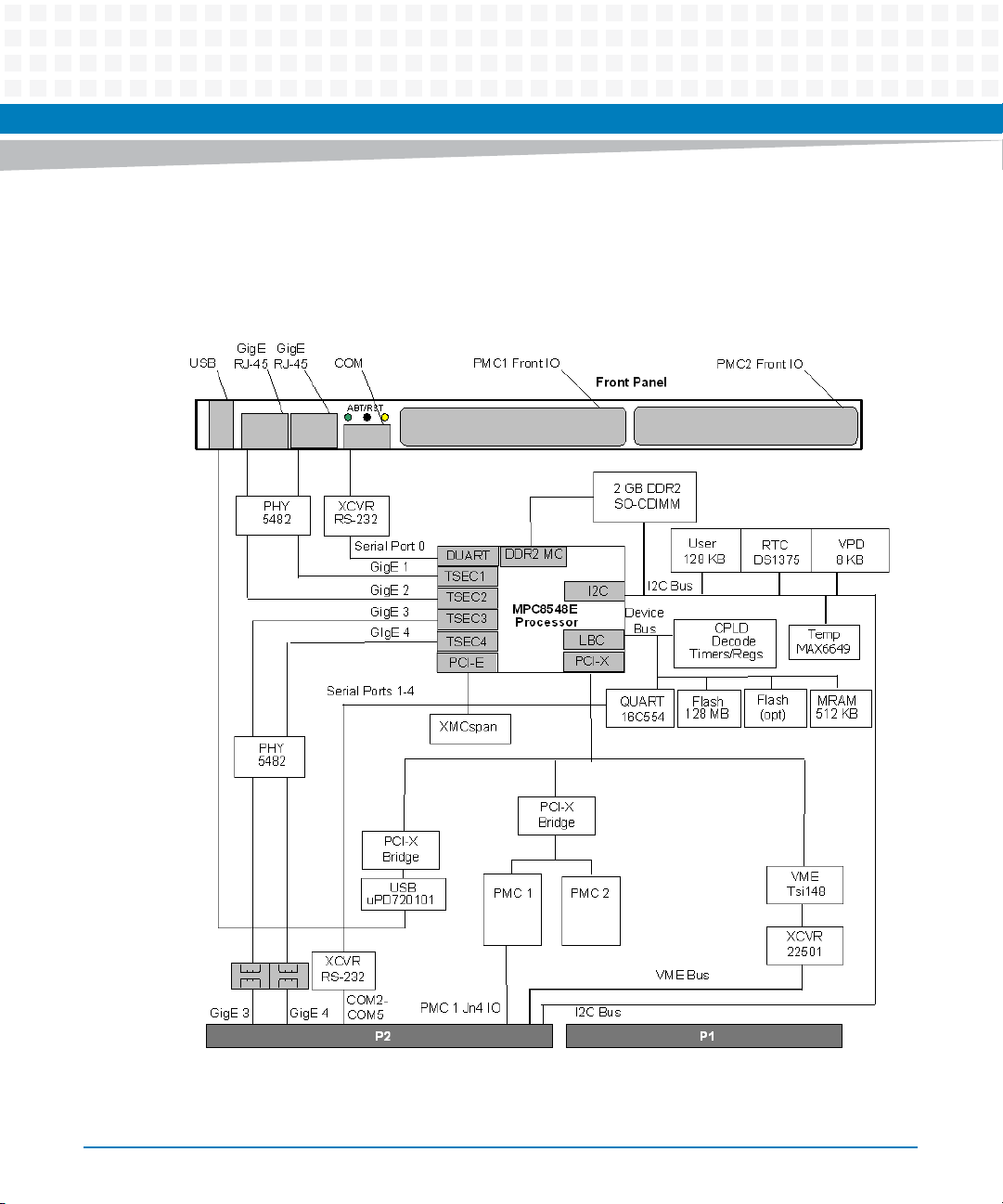
Functional Description
4.2 Block Diagram
The following figure is a block diagram of the MVME4100 architecture.
Figure 4-1 Block Diagram
72
MVME4100 Single Board Computer Installation and Use (6806800H18G)
Page 73

4.3 Processor
The MVME4100 is designed to support the MPC8548E processor. The processor is configured
to operate at 1.3 GHz core frequency with a corresponding 533 Mb DDR2 memory bus.
The MVME4100 supports the power-on reset (POR) pin sampling method for processor reset
configuration. The states of the various configuration pins on the processor are sampled when
reset is de-asserted to determine the desired operating modes. Combinations of pull-up and
pull-down resistors are used to set the options. Some options are fixed and some are selectable
at build time by installing the proper pull-up/pull-down resistor. Refer to the MPC8548E
reference manual, listed in Appendix B, sRelated Documentation, Manufacturers Documents on
page 119 for additional details and/or programming information.
4.4 I2C Serial Interface and Devices
The MVME4100 provides the following on-board I2C serial devices connected to the
MPC8548E I2C controller 0 interface:
Functional Description
8 KB serial EEPROM for VPD
Two 64 KB serial EEPROMs for user configuration data storage
One 256 byte serial EEPROM on SO-CDIMM for SPD
Maxim DS1375 Real Time Clock
Maxim MAX6649 temperature sensor
8 KB serial EEPROM on RTM VPD
The RTC implemented on the MVME4100 provides an alarm interrupt routed to the MPC8548E
PIC through the control PLD. A DS32KHz temperature controlled crystal oscillator provides the
RTC clock reference. A battery backup circuit for the RTC is provided on-board.
The Maxim digital temperature sensor measures of temperature of the board and also
connects to the temperature diode on the MPC8548E. The temperature sensor also provides
an alarm interrupt routed to the MPC8548E PIC through the control PLD.
The I2C interface is routed to the P2 connector for access to the serial EEPROM located on the
transition module. The device address for the transition module serial EEPROM is user
selectable using the configuration switches. Refer to Chapter 5, Transition Module for
information on the switches.
MVME4100 Single Board Computer Installation and Use (6806800H18G)
73
Page 74

Functional Description
For programming information, see the MVME4100 Single Board Computer Programmer’s
Reference.
4.5 System Memory
The MVME4100 includes one SO-CDIMM socket. The SO-CDIMM socket supports 1 GByte and
2 GByte DDR2 SDRAM modules. The MVME4100 supports memory speeds up to DDR533.
4.6 Timers
Timing functions for the MVME4100 are provided by four global high-resolution timers
integrated into the MPC8548E plus four additional independent 32-bit timers in a PLD.
The four integrated 32-bit timers are clocked by the RTC input which is driven by a 1 MHz clock.
Refer to the MPC8548E reference manual, listed in Appendix B, sRelated Documentation,
Manufacturers Documents on page 119 for additional details and/or programming information.
The clock source for the four 32-bit timers in the PLD is 25 MHz. The timer prescaler must be
configured to generate a 1 MHz timer reference. For programming information, see
MVME4100 Single Board Computer Programmer’s Reference.
4.7 Ethernet Interfaces
The MVME4100 provides four 10/100/1000 Mbps full-duplex Ethernet interfaces using the
MPC8548E Ethernet Controllers. Two Broadcom BCM5482S PHYs are used. The Ethernet ports
on the MPC8548E are configured to operate in RGMII mode. Two Gigabit Ethernet interfaces
are routed to front panel RJ-45 connectors with integrated LEDs for speed and activity
indication. The other two Gigabit Ethernet interfaces are routed to P2 for rear I/O. For
programming information, see MVME4100 Single Board Computer Programmer’s Reference.
74
MVME4100 Single Board Computer Installation and Use (6806800H18G)
Page 75

4.8 Local Bus Interface
The MVME4100 uses the MPC8548E Local Bus Controller (LBC) for access to on-board flash and
I/O registers. The LBC has programmable timing modes to support devices of different access
times, as well as device widths of 8, 16, and 32 bits. The MVME4100 uses the LBC in GPCM
mode to interface to two physical banks of on-board flash, an on-board Quad UART (QUART),
an MRAM, and on-board 32-bit timers along with control/status registers. Access timing for
each device type is programmable and depends on the device timing data found in the VPD
during initialization.
A hardware flash bank write protect switch is provided on the MVME4100 to enable write
protection of the NOR Flash. Regardless of the state of the software flash write protect bit in
the NOR Flash Control/Status register, write protection is enabled when this switch is ON.
When this switch is OFF, write protection is controlled by the state of the software flash write
protect bits and can only be disabled by clearing this bit in the NOR Flash Control/Status
register. Note that the F_WE_HW bit reflects the state of the switch and is only software
readable whereas the F_WP_SW bit supports both read and write operations.
Functional Description
The MVME4100 provides a dual boot option for booting from one of two separate boot images
in the boot flash bank which are referred to as boot block A and boot block B. Boot blocks A and
B are each 1 MB in size and are located at the top (highest address) 2 MB of the boot flash
memory space. Block A is located at the highest 1 MB block and block B is the next highest 1 MB
block. A flash boot block switch is used to select between boot block A and boot block B. When
the switch is OFF, the flash memory map is normal and block A is selected. When the switch is
ON, block B is mapped to the highest address. The MAP_SELECT bit in the flash Control/Status
register can disable the jumper and restore the memory map to the normal configuration with
block A selected.
4.8.1 Flash Memory
The MVME4100 is designed to provide 128 MB of soldered-on NOR flash memory. Two
Spansion +3.3 V devices are configured to operate in 16-bit mode to form a 32-bit flash bank.
This flash bank is also the boot bank and is connected to LBC Chip Select 0 and 1.
Also included is a second bank of NAND flash, up to 16 GB, connected to LBC Chip Select 2. The
VPD flash packet(s) will determine which devices are populated and the size of the devices.
Programming details can be found in the MVME4100 Single Board Computer Programmer’s
Reference manual.
MVME4100 Single Board Computer Installation and Use (6806800H18G)
75
Page 76

Functional Description
4.8.2 NVRAM
The MVME4100 includes one Freescale 512 MB MRAM device connected to the MPC8548E
device control bus to provide a non-volatile memory that has unlimited writes, fast access and
long term data retention without power. The MRAM device selected is also an extended
temperature device with an operating range from -40 °C to 105 °C/-40 °F to +221 °F. The
MRAM is organized as 256 K by 16. Refer to the data sheet for additional information.
4.8.3 Quad UART (QUART)
The MVME4100 contains one Quad UART device connected to the MPC8548E device control
bus to provide additional asynchronous serial ports. The Quad UART provides four
asynchronous serial ports which are routed to the P2 connector. The TTL-level signals of RX, TX,
CTS, and RTS from each port are routed through on-board RS-232 drivers and receivers to the
P2 connector where the signals can be picked up by a transition module. The reference clock
frequency for the QUART is 1.8432 MHz. All UART ports are capable of signaling at up to
115 Kbaud. Refer to the ST16C554D data sheet for additional details and/or programming
information.
4.8.4 Control and Timers PLD
The MVME4100 Control and Timers PLD resides on the local bus. The Control and Timers PLD
provides the following functions on the board:
Local bus address latch
Chip selects for flash banks, MRAM, and Quad UART
System control and status registers
Four 32-bit tick timers
Watch Dog Timer
RTC 1 MHz reference clock
76
MVME4100 Single Board Computer Installation and Use (6806800H18G)
Page 77

4.9 DUART Interface
The MVME4100 provides a front access asynchronous serial port interface using Serial Port 0
from the MPC8548E DUART. The T TL-level signals SIN, SOUT, RTS and CTS from Serial Port 0 are
routed through on-board RS-232 drivers and receivers to the mini DB-9 front panel connector.
4.10 PCI-X Port
The PCI-X port on the MPC8548E connects to the TSi148 VMEbus interface and two PCI-X to
PCI-X bridges, PLX PCI6520. The main PCI bus can be configured for 100 MHz PCI-X or 66 MHz
PCI operation.
The secondary side of the first bridge connects to the two PMC sites and is configured
dynamically, with onboard logic, to operate in 33/66 MHz PCI or 66/100 MHz PCI-X mode
depending on the PMCs installed. The secondary side of the second bridge connects to the USB
controller and is configured for 33 MHz PCI mode since the USB controller is only 33 MHz
capable.
Functional Description
4.10.1 Tsi148 VME Controller
The VMEbus interface for the MVME4100 is provided by the Tsi148 VMEbus controller. The
Tsi148 provides the required VME, VME extensions, and 2eSST functions. TI SN74VMEH22501
transceivers are used to buffer the VME signals between the Tsi148 and the VME backplane.
Refer to the Tsi148 user's manual for additional details and/or programming information.
4.10.2 USB
The NEC uPD720101 USB 2.0 Host Controller provides USB ports with integrated transceivers
for connectivity with any USB compliant device or hub. USB channel 1 is routed to a single USB
connector located at the front panel. DC power to the front panel USB port is supplied via a USB
power switch which provides soft-start, current limiting, over current detection, and power
enable for port 1. Refer to the uPD720101 data sheet for additional details and/or
programming information.
MVME4100 Single Board Computer Installation and Use (6806800H18G)
77
Page 78

Functional Description
4.11 XMC Expansion
The MVME4100 provides an additional XMC/PMC module capability through the use of a
78-pin stacking connector. This connector is connected to the PCI Express port on the
processor. Up to four additional XMC/PMC modules may be added by using two expansion
boards. Refer to the XMCspan manual for additional details and/or programming information.
4.12 Power Supplies
The MVME4100 on-board voltages are generated using Linear Tech LTC3828 dual output two
phase controllers and LTC3416 single output controllers. The following sections detail the
MVME4100 power requirements.
4.12.1 Power Sequencing
In order to meet the power sequencing requirements of the various components on the
MVME4100, the power supply controllers implement voltage tracking which allows the power
supply outputs to track each other coincidentally during power up and power down. The
+3.3 V supply output is used as the tracking reference. All supply outputs will reach their final
values within 20 milliseconds during power up.
4.12.2 Power Supply Monitor
Logic is provided on-board to monitor the PGOOD signal from the LTC3828 and LTC3416
regulators to determine if the power supply outputs are within tolerance. If any of the power
supplies fail, this logic shuts off the power supplies to avoid any component damage. If the
+5.0 V power supply is still good during a fail condition, a planar red LED (PWR FAIL D9) is
illuminated to indicate the power supply fail condition.
4.12.3 Power Supply Filtering and Fusing
Each of the switching power supply inputs on the MVME4100 will have an inductor to reduce
switching noise from being fed back onto the +5.0 V input. The LTC3828 supplies will each have
a 10 A fuse to protect the supplies from over-current in case of component failure.
78
MVME4100 Single Board Computer Installation and Use (6806800H18G)
Page 79
4.13 Clock Distribution
The clock function generates and distributes all of the clocks required for system operation.
The PCI-E clocks are generated using an eight output differential clock driver. The PCI/PCI-X bus
clocks are generated by the bridge chips from the PCI-E clock. Additional clocks required by
individual devices are generated near the devices using individual oscillators. For clock
assignments, refer to the MVME4100 Single Board Computer Programmer’s Reference manual.
4.13.1 System Clock
The system clock is driven by an oscillator. The following table defines the clock frequencies.
Table 4-1 Clock Frequencies
SYSCLK Core MPX (Platform) DDR2
66.67 MHz 1.3 GHz 533 MHz 266 MHz
Functional Description
4.13.2 Real Time Clock Input
The RTC clock input is driven by a 1 MHz clock generated by the Control and Timers PLD. This
provides a fixed clock reference for the MPC8548E PIC timers which software can use as a
known timing reference.
4.13.3 Local Bus Controller Clock Divisor
The Local Bus Controller (LBC) clock output is connected to the PLD but is not used by the
internal logic.
4.14 Reset Control Logic
There are multiple sources of reset on the MVME4100. The following sources generate a board
level reset:
Power-up
Reset switch
MVME4100 Single Board Computer Installation and Use (6806800H18G)
79
Page 80

Functional Description
Watchdog timer
System control register (BRD_RST)
VMEbus reset
A board level hard reset generates a reset for the entire SBC including the processor, local
PCI/PCI-X buses, Ethernet PHYs, serial ports, flash devices, and PLD(s). If the MVME4100 is
configured as the VME system controller, the VMEbus and local Tsi148 reset input are also
reset.
4.15 Real Time Clock Battery
There is an on-board battery holder that provides easy replacement of a +3.0 V button cell
lithium battery (BR2325) which provides back-up power to the on-board Real Time Clock. A
battery switching circuit provides automatic switching between the +3.3 V and battery
voltages.
4.16 Debug Support
The MVME4100 provides a boundary scan header for boundary scan test access and device
programming. The MVME4100 also provides a separate standard COP header for processor
COP emulation. A signal from the boundary scan header controls a set of buffers that isolate
the MPC8548E onto a single device chain separate from the Boundary Scan chain containing
all of the scannable devices. This is a requirement of some COP debuggers to allow emulator
support for the MPC8548E.
80
MVME4100 Single Board Computer Installation and Use (6806800H18G)
Page 81

Transition Module
5.1 Overview
This chapter provides information on the MVME7216E transition module’s features. It also
includes a drawing of the module showing the components and rear panel connectors.
Chapter 5
MVME4100 Single Board Computer Installation and Use (6806800H18G)
81
Page 82
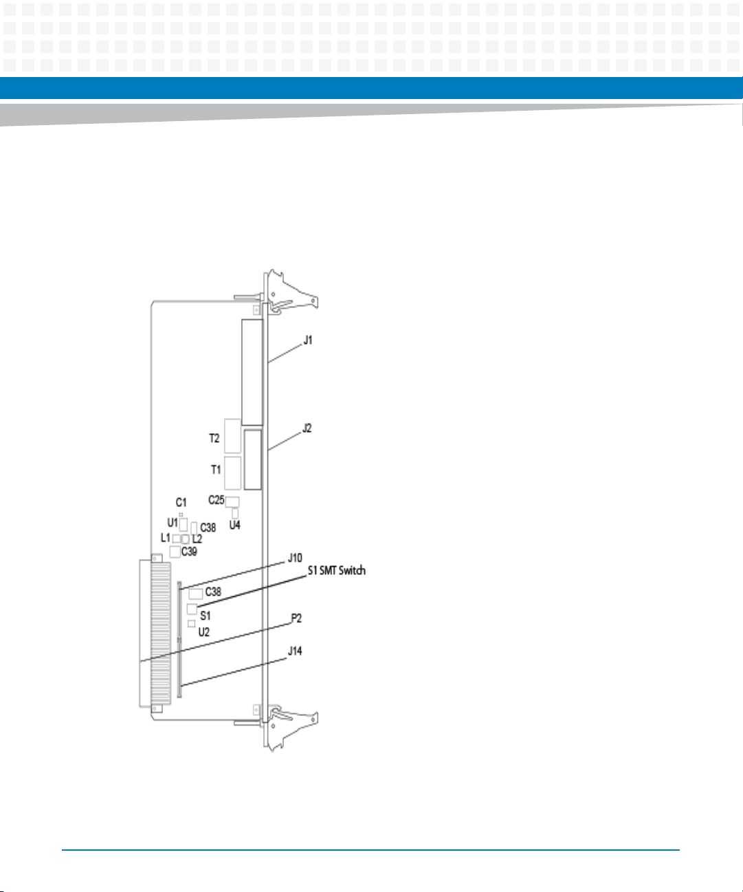
Transition Module
5.2 Transition Module Layout
The following illustration shows the component layout and connectors on the MVME7216E
transition module.
Figure 5-1 Component Layout
82
MVME4100 Single Board Computer Installation and Use (6806800H18G)
Page 83
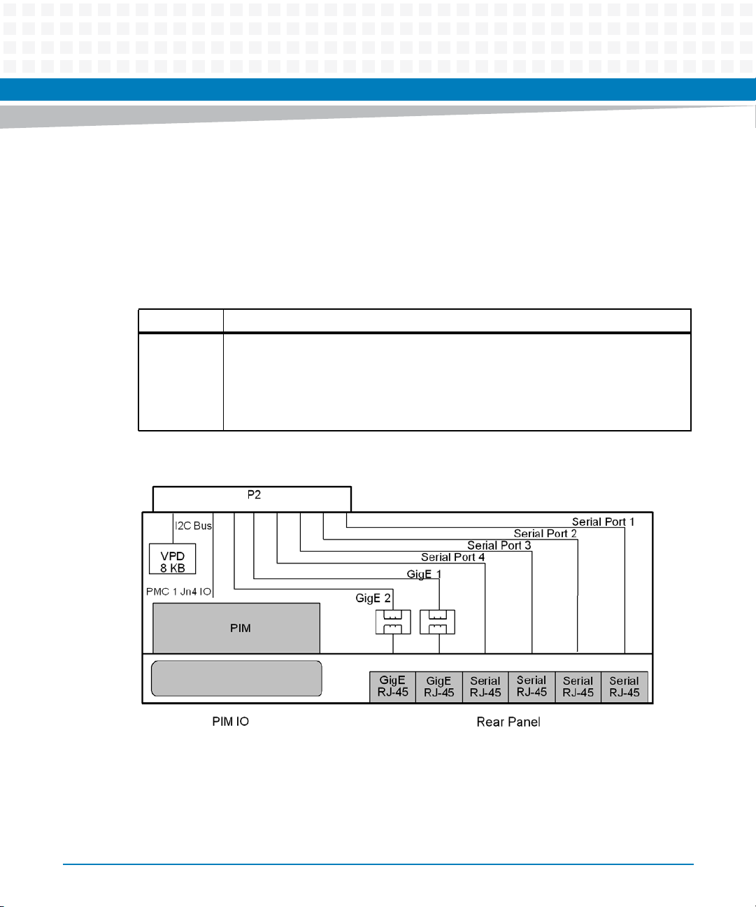
5.3 Features
The MVME7216E transition module is for I/O routing through the rear of a compact VMEbus
chassis. It connects directly to the VME backplane in chassis’ with an 80 mm deep rear
transition area. The MVME7216E is designed for use with the host MVME4100 board. It has the
following features:
Table 5-1 Transition Module Features
Function Features
I/O One five-row P2 backplane connector for serial and Ethernet I/O passed from the SBC
Transition Module
Four RJ-45 connectors for rear panel I/O: four asynchronous serial channels
Two RJ-45 connectors with integrated LEDs for rear panel I/O: two 10/100/1000
Ethernet channels
One PIM site with rear panel I/O
Figure 5-2 Block Diagram
MVME4100 Single Board Computer Installation and Use (6806800H18G)
83
Page 84
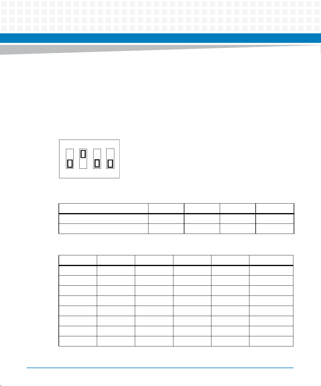
Transition Module
5.4 SEEPROM Address Switch, S1
A 4-position SMT configuration switch is located on the MVME7216E transition module to set
the device address of the RTM serial EEPROM device and to control its write protection (if SW4
is OFF, write is enabled). The switch settings are defined in the next table. To see the switch
location, refer to Figure 5-1 on page 82.
Figure 5-3 S1 Switch Positions
ON
1
2
34
Table 5-2 SEEPROM Address Switch Assignments (RTM)
Position SW4 SW3 SW2 SW1
Function WP A(2) A(1) A(0)
Default (OFF) 0111
Table 5-3 Switch Settings and Device Addresses
SW4 SW3 SW2 SW1 A(2:0) Device Address
OFF ON ON ON 000 $A0
OFF ON ON OFF 001 $A2
OFF ON OFF ON 010 $A4
OFF ON OFF OFF 011 $A6
OFF OFF ON ON 100 $A8
OFF OFF ON OFF 101 $AA (default)
OFF OFF OFF ON 110 $AC
OFF OFF OFF OFF 111 $AE
84
MVME4100 Single Board Computer Installation and Use (6806800H18G)
Page 85
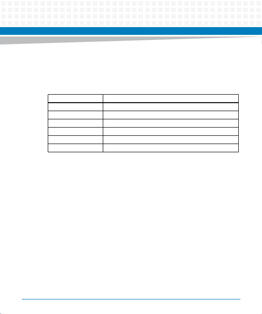
5.5 Rear Panel Connectors
The MVME7216E transition module provides the following connectors. All connectors use
standard pin assignments in compliance with the VMEbus specifications.
Table 5-4 Transition Module Connectors
Connector Function
J1A, J1B, J1C, J1D COM port connectors
J2A 10/100/1000Mb/s Ethernet connector
J2B 10/100/1000Mb/s Ethernet connector
J10 PIM power/ground
J14 PIM I/O
P2 VME backplane connector
Transition Module
MVME4100 Single Board Computer Installation and Use (6806800H18G)
85
Page 86
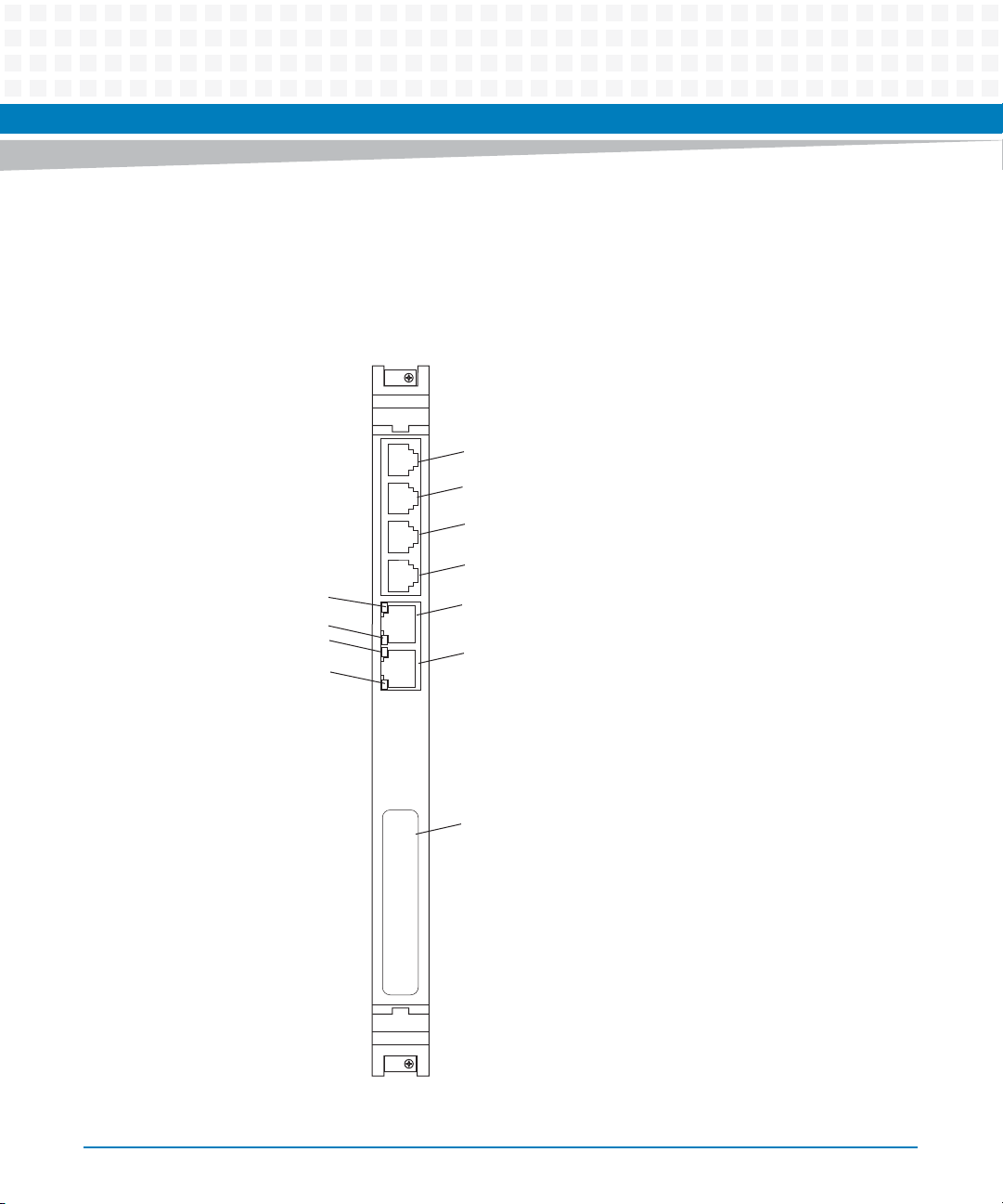
Transition Module
PMC I/O (PIM) connector J10 routes only power and ground from VME P2 connector. There are
no host I/O signals on this connector. The MVME4100 routes PMC I/O from J14 of PMC Slot 1
to VME P2 rows A and C. The MVME7216E routes these signals (pin-for-pin) from VME P2 to
PMC I/O module connector J14.
Figure 5-4 Rear Panel Connectors and LEDs
COM2
COM3
COM4
COM5
ACT
SPEED
ACT
SPEED
G Enet 1
G Enet 2
PMC Site
86
MVME4100 Single Board Computer Installation and Use (6806800H18G)
Page 87
Transition Module
There are two sets of ACT and SPEED LEDs, one set for each Ethernet connector. They are
described in the next table.
Table 5-5 Transition Module LEDs
LED Function
ACT Activity for Ethernet or Gigabit E Ethernet connector
SPEED 10/100/1000Mb/s of Ethernet connectors
5.5.1 MVME7216E PMC I/O Module (PIM) Connectors (J10, J14)
PMC Host I/O connector J10 routes only power and ground from VME P2. There are no Host I/O
signals on this connector. The MVME4100 routes PMC I/O from J14 of PMC Slot 1 to VME P2
rows A and C. The MVME7216E routes these signals (pin-for-pin) from VME P2 to PMC I/O
Module connector J14. See Table 5-6 and Table 3-8 for the pin assignments.
Table 5-6 MVME721 Host I/O Connector (J10) Pin Assignments
Pin Signal Signal Pin
1 No Connect No Connect 2
3 No Connect No Connect 4
5 +5V No Connect 6
7 No Connect No Connect 8
9 No Connect +3.3V 10
11 No Connect No Connect 12
13 GND No Connect 14
15 No Connect No Connect 16
17 No Connect GND 18
19 No Connect No Connect 20
21 +5V No Connect 22
23 No Connect No Connect 24
25 No Connect +3.3V 26
27 No Connect No Connect 28
MVME4100 Single Board Computer Installation and Use (6806800H18G)
87
Page 88
Transition Module
Table 5-6 MVME721 Host I/O Connector (J10) Pin Assignments (continued)
Pin Signal Signal Pin
29 GND No Connect 30
31 No Connect No Connect 32
33 No Connect GND 34
35 No Connect No Connect 36
37 +5V No Connect 38
39 No Connect No Connect 40
41 No Connect +3.3V 42
43 No Connect No Connect 44
45 GND No Connect 46
47 No Connect No Connect 48
49 No Connect GND 50
88
51 No Connect No Connect 52
53 +5V No Connect 54
55 No Connect No Connect 56
57 No Connect +3.3V 58
59 No Connect No Connect 60
61 No Connect No Connect 62
63 No Connect No Connect 64
MVME4100 Single Board Computer Installation and Use (6806800H18G)
Page 89
5.5.2 Ethernet Connectors (GIGE/J41B, GIGE/J2B,GIGE/J2A)
The MVME4100 routes two 10/100/1000Mb/s full duplex Ethernet interfaces to the VMEbus
P2 connector. The MVME7216E routes these from the P2 connector to the RJ-45 connectors on
RTM panel. These connectors include integrated LEDs for speed and activity indication. The pin
assignments for these connectors are as follows:
Table 5-7 Ethernet Connectors Pin Assignment
Pin # Signal 1000 Mb/s 10/100 Mb/s
1 MDIO0+ _DA+ TD+
2 MDIO0- _DA- TD-
3 MDIO1+ _DB+ RD+
4 MDIO1- _DC+ Not Used
5 MDIO2+ _DC- Not Used
Transition Module
6 MDIO2- _DB- RD-
7 MDIO3+ _DD+ Not Used
8 MDIO3- _DD- Not Used
5.5.3 Serial Port Connectors (COM1/J41A, COM2–COM5/J2A-D)
The MVME4100 routes four asynchronous serial port interfaces, SP1 – SP4, to the VMEbus P2
connector. The MVME7216E routes these from the P2 connector to the RJ-45 connectors on
RTM panel. The pin assignments for these connectors are as follows:
Table 5-8 COM Port Connector Pin Assignments
Pin Signal
1 No connect
2RTS
3GND
4TX
5RX
6GND
MVME4100 Single Board Computer Installation and Use (6806800H18G)
89
Page 90
Transition Module
Table 5-8 COM Port Connector Pin Assignments (continued)
Pin Signal
7CTS
8 No connect
5.6 PMC Input/Output Module
If a PMC Input/output Module (PIM) has already been installed on the MVME7216E, or you are
installing a transition module as it has been shipped from the factory, disregard this procedure
and refer to Transition Module on page 38.
Procedure
For PIM installation, perform the following steps:
1. Attach an ESD strap to your wrist.
2. Attach the other end of the ESD strap to the chassis as a ground.
The ESD strap must be secured to your wrist and to ground throughout the
procedure.
3. Carefully remove the transition module from its packaging and lay it flat on a stable
surface.
4. Remove the PIM filler from the front panel of the transition module.
5. Slide the face plate (front bezel) of the PIM module into the front panel opening
from behind and place the PIM module on top of the transition module, aligned
with the appropriate two PIM connectors. The two connectors on the underside of
the PIM module should then connect smoothly with the corresponding connectors
on the transition module (J10 and J14).
6. Insert the four short Phillips screws, provided with the PIM, through the holes on
the bottom side of the transition module into the PIM front bezel and rear
standoffs. Tighten the screws.
90
MVME4100 Single Board Computer Installation and Use (6806800H18G)
Page 91
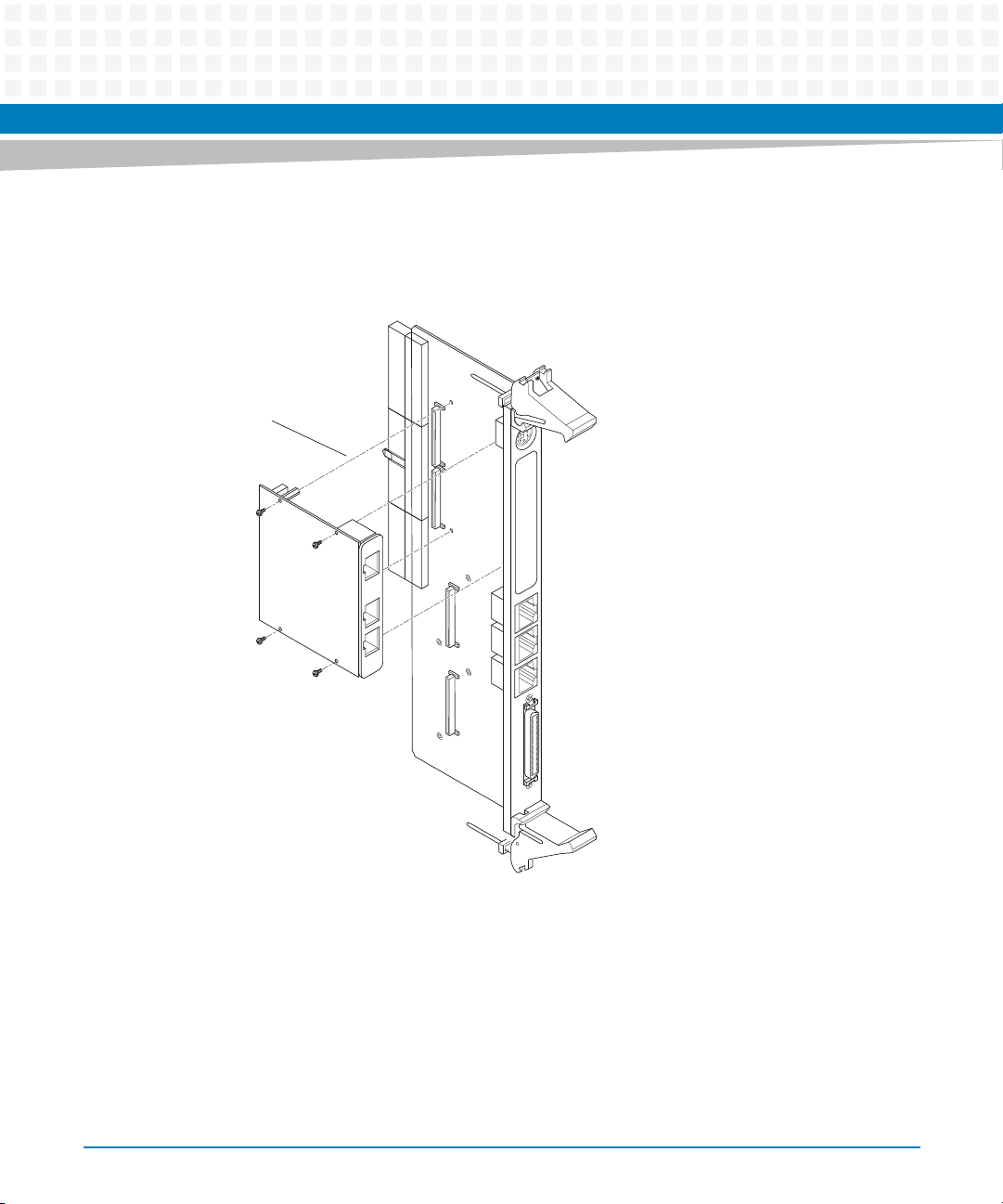
Transition Module
PIM Alignment
Refer to the following figure for proper screw/board alignment. The example below
may not accurately represent your MVME7216E.
Figure 5-5 Installing the PIM
MVME4100 Single Board Computer Installation and Use (6806800H18G)
91
Page 92

Transition Module
92
MVME4100 Single Board Computer Installation and Use (6806800H18G)
Page 93

MOTLoad Firmware
6.1 Overview
The MOTLoad firmware package serves as a board power-up and initialization package, as well
as a vehicle from which user applications can be booted. A secondary function of the MOTLoad
firmware is to serve in some respects as a test suite providing individual tests for certain
devices. This chapter includes a list of standard MOTLoad commands, the default VME and
firmware settings that are changeable by the user, remote start, and the alternate boot
procedure.
MOTLoad is controlled through an easy-to-use, UNIX-like, command line interface. The
MOTLoad software package is similar to many end-user applications designed for the
embedded market, such as the real time operating systems currently available.
Refer to the MOTLoad Firmware Package User’s Manual, listed in Appendix B, sRelated
Documentation, for more details.
Chapter 6
6.2 Implementation and Memory Requirements
The implementation of MOTLoad and its memory requirements are product specific. The
MVME4100 single-board computer (SBC) is offered with a range of memory (for example,
DRAM or flash). Typically, the smallest amount of on-board DRAM that a SBC has is 32 MB. Each
supported product line has its own unique MOTLoad binary image(s). Currently the largest
MOTLoad compressed image is less than 1 MB in size.
6.3 MOTLoad Commands
MOTLoad supports two types of commands (applications): utilities and tests. Both types of
commands are invoked from the MOTLoad command line in a similar fashion. Beyond that,
MOTLoad utilities and MOTLoad tests are distinctly different.
6.3.1 Utilities
The definition of a MOTLoad utility application is very broad. Simply stated, it is considered a
MOTLoad command if it is not a MOTLoad test. Typically, MOTLoad utility applications are
applications that aid the user in some way (that is, they do something useful). From the
perspective of MOTLoad, examples of utility applications are: configuration, data/status
displays, data manipulation, help routines, data/status monitors, etc.
MVME4100 Single Board Computer Installation and Use (6806800H18G)
93
Page 94

MOTLoad Firmware
Operationally, MOTLoad utility applications differ from MOTLoad test applications in several
ways:
Only one utility application operates at any given time (that is, multiple utility applications
cannot be executing concurrently).
Utility applications may interact with the user. Most test applications do not.
6.3.2 Tests
A MOTLoad test application determines whether or not the hardware meets a given standard.
Test applications are validation tests. Validation is conformance to a specification. Most
MOTLoad tests are designed to directly validate the functionality of a specific SBC subsystem
or component. It is possible for a board's component to fail in the user application but pass
specification conformance. These tests validate the operation of such SBC modules as:
dynamic memory, external cache, NVRAM, real time clock, etc.
All MOTLoad tests are designed to validate functionality with minimum user interaction. Once
launched, most MOTLoad tests operate automatically without any user interaction. There are
a few tests where the functionality being validated requires user interaction (that is, switch
tests, interactive plug-in hardware modules, etc.). Most MOTLoad test results (errordata/status-data) are logged, not printed. Test results are not preserved and therefore not
available to user applications subsequent to their execution. All MOTLoad tests/commands
have complete and separate descriptions (refer to the MOTLoad Firmware Package User’s Manual
for this information).
94
All devices that are available to MOTLoad for validation/verification testing are represented by
a unique device path string. Most MOTLoad tests require the operator to specify a test device
at the MOTLoad command line when invoking the test.
A listing of all device path strings can be displayed through the devShow command. If an SBC
device does not have a device path string, it is not supported by MOTLoad and cannot be
directly tested. There are a few exceptions to the device path string requirement, like testing
RAM, which is not considered a true device and can be directly tested without a device path
string. Refer to the devShow command description page in the MOTLoad Firmware Package
User’s Manual.
MVME4100 Single Board Computer Installation and Use (6806800H18G)
Page 95

Most MOTLoad tests can be organized to execute as a group of related tests (a testSuite)
through the use of the testSuite command. The expert operator can customize their
testing by defining and creating a custom testSuite(s). The list of built-in and user-defined
MOTLoad testSuites, and their test contents can be obtained by entering testSuite -d at
the MOTLoad prompt. All testSuites that are included as part of a product specific MOTLoad
firmware package are product specific. For more information, refer to the testSuite
command description page in the MOTLoad Firmware Package User’s Manual.
Test results and test status are obtained through the testStatus, errorDisplay, and
taskActive commands. Refer to the appropriate command description page in the
MOTLoad Firmware Package User’s Manual for more information.
6.3.3 Command List
The following table provides a list of all current MOTLoad commands. Products supported by
MOTLoad may or may not employ the full command set. Typing help at the MOTLoad
command prompt will display all commands supported by MOTLoad for a given product.
MOTLoad Firmware
Table 6-1 MOTLoad Commands
Command Description
as One-Line Instruction Assembler
bcb
bch
bcw
bdTempShow Display Current Board Temperature
bfb
bfh
bfw
blkCp Block Copy
blkFmt Block Format
blkRd Block Read
blkShow Block Show Device Configuration Data
blkVe Block Verify
blkWr Block Write
MVME4100 Single Board Computer Installation and Use (6806800H18G)
Block Compare Byte/Halfword/Word
Block Fill Byte/Halfword/Word
95
Page 96

MOTLoad Firmware
Table 6-1 MOTLoad Commands (continued)
Command Description
bmb
bmh
bmw
br Assign/Delete/Display User-Program Break-Points
Block Move Byte/Halfword/Word
bsb
bsh
bsw
bvb
bvh
bvw
cdDir ISO9660 File System Directory Listing
cdGet ISO9660 File System File Load
clear Clear the Specified Status/History Table(s)
cm Turns on Concurrent Mode
csb
csh
csw
devShow Display (Show) Device/Node Table
diskBoot Disk Boot (Direct-Access Mass-Storage Device)
downLoad Down Load S-Record from Host
ds One-Line Instruction Disassembler
echo Echo a Line of Text
elfLoader ELF Object File Loader
Block Search Byte/Halfword/Word
Block Verify Byte/Halfword/Word
Calculates a Checksum Specified by Command-line Options
96
errorDisplay Display the Contents of the Test Error Status Table
eval Evaluate Expression
execProgram Execute Program
fatDir FAT File System Directory Listing
fatGet FAT File System File Load
MVME4100 Single Board Computer Installation and Use (6806800H18G)
Page 97

MOTLoad Firmware
Table 6-1 MOTLoad Commands (continued)
Command Description
fdShow Display (Show) File Discriptor
flashLock Flash Memory Sector Lock
flashProgram Flash Memory Program
flashShow Display Flash Memory Device Configuration Data
flashUnlock Flash Memory Sector Unlock
gd Go Execute User-Program Direct (Ignore Break-Points)
gevDelete Global Environment Variable Delete
gevDump Global Environment Variable(s) Dump (NVRAM Header + Data)
gevEdit Global Environment Variable Edit
gevInit Global Environment Variable Area Initialize (NVRAM Header)
gevList Global Environment Variable Labels (Names) Listing
gevShow Global Environment Variable Show
gn Go Execute User-Program to Next Instruction
go Go Execute User-Program
gt Go Execute User-Program to Temporary Break-Point
hbd Display History Buffer
hbx Execute History Buffer Entry
help Display Command/Test Help Strings
l2CacheShow Display state of L2 Cache and L2CR register contents
l3CacheShow Display state of L3 Cache and L3CR register contents
mdb
mdh
mdw
memShow Display Memory Allocation
mmb
mmh
mmw
mpuFork Execute program from idle processor
MVME4100 Single Board Computer Installation and Use (6806800H18G)
Memory Display Bytes/Halfwords/Words
Memory Modify Bytes/Halfwords/Words
97
Page 98

MOTLoad Firmware
Table 6-1 MOTLoad Commands (continued)
Command Description
mpuShow Display multi-processor control structure
mpuStart Start the other MPU
netBoot Network Boot (BOOT/TFTP)
netShow Display Network Interface Configuration Data
netShut Disable (Shutdown) Network Interface
netStats Display Network Interface Statistics Data
noCm Turns off Concurrent Mode
pciDataRd Read PCI Device Configuration Header Register
pciDataWr Write PCI Device Configuration Header Register
pciDump Dump PCI Device Configuration Header Register
pciShow Display PCI Device Configuration Header Register
98
pciSpace Display PCI Device Address Space Allocation
ping Ping Network Host
portSet Port Set
portShow Display Port Device Configuration Data
rd User Program Register Display
reset Reset System
rs User Program Register Set
set Set Date and Time
sromRead SROM Read
sromWrite SROM Write
sta Symbol Table Attach
stl Symbol Table Lookup
stop Stop Date and Time (Power-Save Mode)
taskActive Display the Contents of the Active Task Table
tc Trace (Single-Step) User Program
td Trace (Single-Step) User Program to Address
MVME4100 Single Board Computer Installation and Use (6806800H18G)
Page 99

Table 6-1 MOTLoad Commands (continued)
Command Description
testDisk Test Disk
testEnetPtP Ethernet Point-to-Point
testNvramRd NVRAM Read
testNvramRdWr NVRAM Read/Write (Destructive)
testRam RAM Test (Directory)
testRamAddr RAM Addressing
testRamAlt RAM Alternating
testRamBitToggle RAM Bit Toggle
testRamBounce RAM Bounce
testRamCodeCopy RAM Code Copy and Execute
testRamEccMonitor Monitor for ECC Errors
MOTLoad Firmware
testRamMarch RAM March
testRamPatterns RAM Patterns
testRamPerm RAM Permutations
testRamQuick RAM Quick
testRamRandom RAM Random Data Patterns
testRtcAlarm RTC Alarm
testRtcReset RTC Reset
testRtcRollOver RTC Rollover
testRtcTick RTC Tick
testSerialExtLoop Serial External Loopback
testSeriallntLoop Serial Internal Loopback
testStatus Display the Contents of the Test Status Table
testSuite Execute Test Suite
testSuiteMake Make (Create) Test Suite
testWatchdogTimer Tests the Accuracy of the Watchdog Timer Device
tftpGet TFTP Get
MVME4100 Single Board Computer Installation and Use (6806800H18G)
99
Page 100
MOTLoad Firmware
Table 6-1 MOTLoad Commands (continued)
Command Description
tftpPut TFTP Put
time Display Date and Time
transparentMode Transparent Mode (Connect to Host)
tsShow Display Task Status
upLoad Up Load Binary Data from Target
version Display Version String(s)
vmeCfg Manages user specified VME configuration parameters
vpdDisplay VPD Display
vpdEdit VPD Edit
wait Wait for Test Completion
waitProbe Wait for I/O Probe to Complete
6.4 Using the Command Line Interface
Interaction with MOTLoad is performed via a command line interface through a serial port on
the single board computer, which is connected to a terminal or terminal emulator (for
example, Window’s Hypercomm). The default MOTLoad serial port settings are: 9600 baud,
8 bits, no parity.
The MOTLoad command line interface is similar to a UNIX command line shell interface.
Commands are initiated by entering a valid MOTLoad command (a text string) at the MOTLoad
command line prompt and pressing the carriage-return key to signify the end of input.
MOTLoad then performs the specified action. An example of a MOTLoad command line
prompt is shown below. The MOTLoad prompt changes according to what product it is used on
(for example, MVME6100, MVME3100, MVME4100).
Example:
MVME4100>
If an invalid MOTLoad command is entered at the MOTLoad command line prompt, MOTLoad
displays a message that the command was not found.
100
MVME4100 Single Board Computer Installation and Use (6806800H18G)
 Loading...