

Page 1

MVME7616E Transition Module
Installation and Use
P/N: 6806800A43D
April 2015
Page 2

©
Copyright 2015 Artesyn Embedded Technologies, Inc.
All rights reserved.
Trademarks
Artesyn Embedded Technologies, Artesyn and the Artesyn Embedded Technologies logo are trademarks and service marks of
Artesyn Embedded Technologies, Inc.© 2015 Artesyn Embedded Technologies, Inc. All other product or service names are the
property of their respective owners.
Intel® is a trademark or registered trademark of Intel Corporation or its subsidiaries in the United States and other countries.
Java™ and all other Java-based marks are trademarks or registered trademarks of Oracle America, Inc. in the U.S. and other countries.
Microsoft®, Windows® and Windows Me® are registered trademarks of Microsoft Corporation; and Windows XP™ is a trademark of
Microsoft Corporation.
PICMG®, CompactPCI®, AdvancedTCA™ and the PICMG, CompactPCI and AdvancedTCA logos are registered trademarks of the PCI
Industrial Computer Manufacturers Group.
UNIX® is a registered trademark of The Open Group in the United States and other countries.
Notice
While reasonable efforts have been made to assure the accuracy of this document, Artesyn assumes no liability resulting from any
omissions in this document, or from the use of the information obtained therein. Artesyn reserves the right to revise this document
and to make changes from time to time in the content hereof without obligation of Artesyn to notify any person of such revision or
changes.
Electronic versions of this material may be read online, downloaded for personal use, or referenced in another document as a URL to
an Artesyn website. The text itself may not be published commercially in print or electronic form, edited, translated, or otherwise
altered without the permission of Artesyn.
It is possible that this publication may contain reference to or information about Artesyn products (machines and programs),
programming, or services that are not available in your country. Such references or information must not be construed to mean that
Artesyn intends to announce such Artesyn products, programming, or services in your country.
Limited and Restricted Rights Legend
If the documentation contained herein is supplied, directly or indirectly, to the U.S. Government, the following notice shall apply
unless otherwise agreed to in writing by Artesyn.
Use, duplication, or disclosure by the Government is subject to restrictions as set forth in subparagraph (b)(3) of the Rights in
Technical Data clause at DFARS 252.227-7013 (Nov. 1995) and of the Rights in Noncommercial Computer Software and
Documentation clause at DFARS 252.227-7014 (Jun. 1995).
Contact Address
Artesyn Embedded Technologies Artesyn Embedded Technologies
Marketing Communications Lilienthalstr. 17-19
2900 S. Diablo Way, Suite 190 85579 Neubiberg/Munich
Tempe, Arizona 85282 Germany
Page 3

Contents
Contents
About this Manual . . . . . . . . . . . . . . . . . . . . . . . . . . . . . . . . . . . . . . . . . . . . . . . . . . . . . . . . . . . . . . . . . . . . . . . . 9
1 General Information . . . . . . . . . . . . . . . . . . . . . . . . . . . . . . . . . . . . . . . . . . . . . . . . . . . . . . . . . . . . . . . . . . 13
1.1 Overview . . . . . . . . . . . . . . . . . . . . . . . . . . . . . . . . . . . . . . . . . . . . . . . . . . . . . . . . . . . . . . . . . . . . . . . . . . 13
1.2 Features . . . . . . . . . . . . . . . . . . . . . . . . . . . . . . . . . . . . . . . . . . . . . . . . . . . . . . . . . . . . . . . . . . . . . . . . . . . 13
1.3 General Description . . . . . . . . . . . . . . . . . . . . . . . . . . . . . . . . . . . . . . . . . . . . . . . . . . . . . . . . . . . . . . . . . 13
1.4 Serial Port Interface Modules . . . . . . . . . . . . . . . . . . . . . . . . . . . . . . . . . . . . . . . . . . . . . . . . . . . . . . . . . 15
1.5 P2 Adapter Boards . . . . . . . . . . . . . . . . . . . . . . . . . . . . . . . . . . . . . . . . . . . . . . . . . . . . . . . . . . . . . . . . . . 15
1.6 Three-row P2 Adapter (MVME761-001) . . . . . . . . . . . . . . . . . . . . . . . . . . . . . . . . . . . . . . . . . . . . . . . 16
1.7 Five-Row P2 Adapter (MVME761-011) . . . . . . . . . . . . . . . . . . . . . . . . . . . . . . . . . . . . . . . . . . . . . . . . 17
1.8 Connectors and Cables . . . . . . . . . . . . . . . . . . . . . . . . . . . . . . . . . . . . . . . . . . . . . . . . . . . . . . . . . . . . . . 17
1.9 Specifications . . . . . . . . . . . . . . . . . . . . . . . . . . . . . . . . . . . . . . . . . . . . . . . . . . . . . . . . . . . . . . . . . . . . . . 19
1.10 Cooling Requirements . . . . . . . . . . . . . . . . . . . . . . . . . . . . . . . . . . . . . . . . . . . . . . . . . . . . . . . . . . . . . . 20
1.11 FCC Compliance . . . . . . . . . . . . . . . . . . . . . . . . . . . . . . . . . . . . . . . . . . . . . . . . . . . . . . . . . . . . . . . . . . . . 20
2 Hardware Preparation and Installation . . . . . . . . . . . . . . . . . . . . . . . . . . . . . . . . . . . . . . . . . . . . . . . . . 21
2.1 Overview . . . . . . . . . . . . . . . . . . . . . . . . . . . . . . . . . . . . . . . . . . . . . . . . . . . . . . . . . . . . . . . . . . . . . . . . . . 21
2.2 Unpacking the Hardware . . . . . . . . . . . . . . . . . . . . . . . . . . . . . . . . . . . . . . . . . . . . . . . . . . . . . . . . . . . . 21
2.3 Installing the Serial Interface Modules . . . . . . . . . . . . . . . . . . . . . . . . . . . . . . . . . . . . . . . . . . . . . . . . . 21
2.4 Installing the Transition Module and P2 Adapter . . . . . . . . . . . . . . . . . . . . . . . . . . . . . . . . . . . . . . . . 24
3 Functional Description . . . . . . . . . . . . . . . . . . . . . . . . . . . . . . . . . . . . . . . . . . . . . . . . . . . . . . . . . . . . . . . . 27
3.1 Overview . . . . . . . . . . . . . . . . . . . . . . . . . . . . . . . . . . . . . . . . . . . . . . . . . . . . . . . . . . . . . . . . . . . . . . . . . . 27
3.2 Circuitry . . . . . . . . . . . . . . . . . . . . . . . . . . . . . . . . . . . . . . . . . . . . . . . . . . . . . . . . . . . . . . . . . . . . . . . . . . . 27
3.3 P2 Signal Multiplexing (P2MX) . . . . . . . . . . . . . . . . . . . . . . . . . . . . . . . . . . . . . . . . . . . . . . . . . . . . . . . 29
3.4 Serial Interface Module Circuitry . . . . . . . . . . . . . . . . . . . . . . . . . . . . . . . . . . . . . . . . . . . . . . . . . . . . . . 32
3.5 COM1 and COM2 Asynchronous Serial Ports . . . . . . . . . . . . . . . . . . . . . . . . . . . . . . . . . . . . . . . . . . . 34
3.6 Asynchronous/Synchronous Serial Ports . . . . . . . . . . . . . . . . . . . . . . . . . . . . . . . . . . . . . . . . . . . . . . . 36
4 Connector Pin Assignments . . . . . . . . . . . . . . . . . . . . . . . . . . . . . . . . . . . . . . . . . . . . . . . . . . . . . . . . . . . 41
4.1 Overview . . . . . . . . . . . . . . . . . . . . . . . . . . . . . . . . . . . . . . . . . . . . . . . . . . . . . . . . . . . . . . . . . . . . . . . . . . 41
4.2 P2 Connector . . . . . . . . . . . . . . . . . . . . . . . . . . . . . . . . . . . . . . . . . . . . . . . . . . . . . . . . . . . . . . . . . . . . . . 41
4.3 Asynchronous Serial Port Connectors (J5/J6) . . . . . . . . . . . . . . . . . . . . . . . . . . . . . . . . . . . . . . . . . . . 43
MVME7616E Transition Module Installation and Use (6806800A43D)
3
Page 4

Contents
Contents
Contents
4.4 Asynchronous/Synchronous serial Port connectors (J7/J8) . . . . . . . . . . . . . . . . . . . . . . . . . . . . . . . 43
4.5 Parallel I/O Port Connector (J4) . . . . . . . . . . . . . . . . . . . . . . . . . . . . . . . . . . . . . . . . . . . . . . . . . . . . . . . 45
4.6 Ethernet Connector (J9) . . . . . . . . . . . . . . . . . . . . . . . . . . . . . . . . . . . . . . . . . . . . . . . . . . . . . . . . . . . . . 46
4.7 P2 Adapter Connectors . . . . . . . . . . . . . . . . . . . . . . . . . . . . . . . . . . . . . . . . . . . . . . . . . . . . . . . . . . . . . . 46
4.7.1 3-Row P2 Adapter (J2) . . . . . . . . . . . . . . . . . . . . . . . . . . . . . . . . . . . . . . . . . . . . . . . . . . . . . . . . 46
4.7.2 3-Row P2 Adapter (J3) . . . . . . . . . . . . . . . . . . . . . . . . . . . . . . . . . . . . . . . . . . . . . . . . . . . . . . . . 48
4.7.3 5-Row P2 adapter (J1) . . . . . . . . . . . . . . . . . . . . . . . . . . . . . . . . . . . . . . . . . . . . . . . . . . . . . . . . 49
4.7.4 PMC I/O, 5-Row P2 Adapter (J3) . . . . . . . . . . . . . . . . . . . . . . . . . . . . . . . . . . . . . . . . . . . . . . . . 51
4.7.5 5-Row P2 adapter (J4) . . . . . . . . . . . . . . . . . . . . . . . . . . . . . . . . . . . . . . . . . . . . . . . . . . . . . . . . 52
4
MVME7616E Transition Module Installation and Use (6806800A43D)
Page 5

List of Tables
Table 1-1 SIM Part Numbers . . . . . . . . . . . . . . . . . . . . . . . . . . . . . . . . . . . . . . . . . . . . . . . . . . . . . . . . . . . . . . 15
Table 1-2 MVME761 Transition Module Connectors . . . . . . . . . . . . . . . . . . . . . . . . . . . . . . . . . . . . . . . . . 18
Table 1-3 3-Row P2 Adapter Connectors (MVME761-001) . . . . . . . . . . . . . . . . . . . . . . . . . . . . . . . . . . . . 18
Table 1-4 5-Row P2 Adapter Connectors (MVME761-011) . . . . . . . . . . . . . . . . . . . . . . . . . . . . . . . . . . . . 18
Table 1-5 Transition Module Cables . . . . . . . . . . . . . . . . . . . . . . . . . . . . . . . . . . . . . . . . . . . . . . . . . . . . . . . 19
Table 1-6 MVME761-0x1 Specifications . . . . . . . . . . . . . . . . . . . . . . . . . . . . . . . . . . . . . . . . . . . . . . . . . . . . 19
Table 3-1 P2 signal multiplexing sequence . . . . . . . . . . . . . . . . . . . . . . . . . . . . . . . . . . . . . . . . . . . . . . . . . 31
Table 4-1 P2 Connector Pin Assignments . . . . . . . . . . . . . . . . . . . . . . . . . . . . . . . . . . . . . . . . . . . . . . . . . . 41
Table 4-2 COM1 and COM2 Pin Assignments . . . . . . . . . . . . . . . . . . . . . . . . . . . . . . . . . . . . . . . . . . . . . . . 43
Table 4-3 Serial Port 3 Pin Assignments . . . . . . . . . . . . . . . . . . . . . . . . . . . . . . . . . . . . . . . . . . . . . . . . . . . . 43
Table 4-4 Serial Port 4 Pin Assignments . . . . . . . . . . . . . . . . . . . . . . . . . . . . . . . . . . . . . . . . . . . . . . . . . . . . 44
Table 4-5 Parallel I/O Connector Pin Assignments . . . . . . . . . . . . . . . . . . . . . . . . . . . . . . . . . . . . . . . . . . . 45
Table 4-6 10Base-T/100Base-TX Pin Assignments . . . . . . . . . . . . . . . . . . . . . . . . . . . . . . . . . . . . . . . . . . . 46
Table 4-7 8-bit SCSI Connector (3-Row P2 adapter) . . . . . . . . . . . . . . . . . . . . . . . . . . . . . . . . . . . . . . . . . . 46
Table 4-8 VME Connector (3-Row P2 adapter) . . . . . . . . . . . . . . . . . . . . . . . . . . . . . . . . . . . . . . . . . . . . . . 48
Table 4-9 16-bit SCSI Connector (5-Row P2 adapter) . . . . . . . . . . . . . . . . . . . . . . . . . . . . . . . . . . . . . . . . 49
Table 4-10 PMC I/O Connector (5-Row P2 adapter) . . . . . . . . . . . . . . . . . . . . . . . . . . . . . . . . . . . . . . . . . . . 51
Table 4-11 VME Connector (3-Row P2 adapter) . . . . . . . . . . . . . . . . . . . . . . . . . . . . . . . . . . . . . . . . . . . . . . 52
MVME7616E Transition Module Installation and Use (6806800A43D)
5
Page 6

List of Tables
6
MVME7616E Transition Module Installation and Use (6806800A43D)
Page 7

List of Figures
Figure 1-1 RTM Front Panel and Components Side . . . . . . . . . . . . . . . . . . . . . . . . . . . . . . . . . . . . 14
Figure 1-2 Three Row P2 Adapter . . . . . . . . . . . . . . . . . . . . . . . . . . . . . . . . . . . . . . . . . . . . . . . . . . . 16
Figure 1-3 Five Row P2 Adapter . . . . . . . . . . . . . . . . . . . . . . . . . . . . . . . . . . . . . . . . . . . . . . . . . . . . . 17
Figure 2-1 Serial Port Interface Jumper Setting . . . . . . . . . . . . . . . . . . . . . . . . . . . . . . . . . . . . . . . 21
Figure 2-2 SIM Configuration . . . . . . . . . . . . . . . . . . . . . . . . . . . . . . . . . . . . . . . . . . . . . . . . . . . . . . . 22
Figure 2-3 Installing the SIM . . . . . . . . . . . . . . . . . . . . . . . . . . . . . . . . . . . . . . . . . . . . . . . . . . . . . . . . 23
Figure 2-4 Chassis Connections . . . . . . . . . . . . . . . . . . . . . . . . . . . . . . . . . . . . . . . . . . . . . . . . . . . . . 25
Figure 3-1 Transition Module Block Diagram . . . . . . . . . . . . . . . . . . . . . . . . . . . . . . . . . . . . . . . . . 28
Figure 3-2 3-Row DIN Backplane P2 Adapter Block Diagram . . . . . . . . . . . . . . . . . . . . . . . . . . . . 29
Figure 3-3 5-Row DIN Backplane P2 Adapter Block Diagram . . . . . . . . . . . . . . . . . . . . . . . . . . . . 29
Figure 3-4 Multiplex Signal Timing Chart . . . . . . . . . . . . . . . . . . . . . . . . . . . . . . . . . . . . . . . . . . . . 32
Figure 3-5 EIA-574 DTE Port Configuration . . . . . . . . . . . . . . . . . . . . . . . . . . . . . . . . . . . . . . . . . . . 35
Figure 3-6 EIA232-DCE Configuration Port 3 . . . . . . . . . . . . . . . . . . . . . . . . . . . . . . . . . . . . . . . . . 37
Figure 3-7 EIA232-DCE Configuration Port 4 . . . . . . . . . . . . . . . . . . . . . . . . . . . . . . . . . . . . . . . . . 38
Figure 3-8 EIA232-DTE Configuration Port 3 . . . . . . . . . . . . . . . . . . . . . . . . . . . . . . . . . . . . . . . . . . 39
Figure 3-9 EIA232-DTE Configuration Port 4 . . . . . . . . . . . . . . . . . . . . . . . . . . . . . . . . . . . . . . . . . . 40
MVME7616E Transition Module Installation and Use (6806800A43D)
7
Page 8

List of Figures
8
MVME7616E Transition Module Installation and Use (6806800A43D)
Page 9

About this Manual
Overview of Contents
This manual is divided into the following chapters and appendices:
Chapter 1, General Information, on page 13
Chapter 2, Hardware Preparation and Installation, on page 21
Chapter 3, Functional Description, on page 27
Chapter 4, Connector Pin Assignments, on page 41
MVME7616E Transition Module Installation and Use provides general information, hardware
preparation, installation instructions and support information for the MVME7616E-001 and
MVME7616E-011 Transition Modules. These transition modules are used as the interface
between the variants of the MVME51005E and MVME55006E Single Board Computers. A P2
adapter module and cable are supplied with the MVME7616E. The MVME7616E will hereafter
be referred to as the MVME761.
As of the printing date of this manual, these I/O module models are available:
Model Number Description
MVME7616E-001
MVME7616E-011
MVME761P26E-001
MVME761P2-6E011
Related Product
MVME51005E
MVME51105E
MVME55006E MVME Series MVME55006E Single Board Computer
IPMC7616E-001
IPMC7616E-002
SIM232DCE5E
SIM232DTE5E
MVME7616E Transition Module Installation and Use (6806800A43D)
3-Row Rear Transition Module and P2 Adaptor
5-Row Rear Transition Module and P2 Adaptor
3-Row, P2 Adapter Module Only
5-Row, P2 Adapter Module Only
MVME Series MVME51005E Single Board Computer
Multifunction rear I/O PMC module; Ultra-Wide SCSI, one parallel port,
three asynchronous and one synchronous/asynchronous serial port
EIA232-DCE serial interface module
EIA232-DTE serial interface module
9
Page 10
About this Manual
Abbreviations
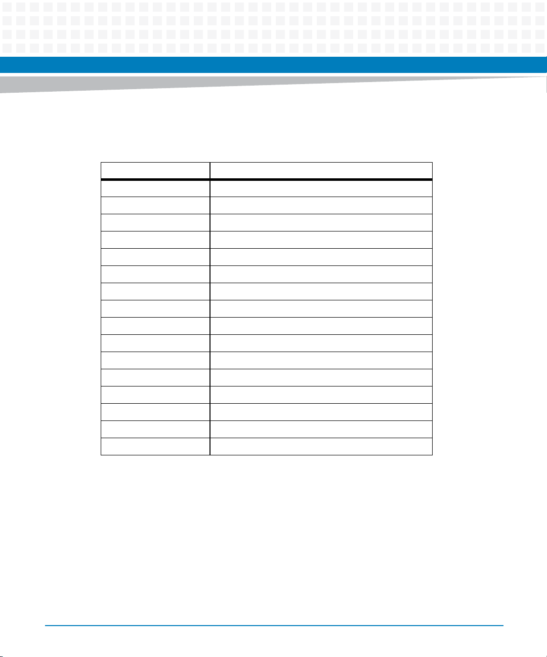
This document uses the following abbreviations:
Abbreviation Description
CFM Cubic Feet per Minute
DCE Data Communications Equipment
DIN Deutsches Insitut für Normung eV
DTE Data Terminal Equipment
EMI Electro-Magnetic Interference
ESD Electro-Static Discharge
FCC Federal Communications Commission
GND Ground
IC Integrated Circuit
About this Manual
10
IEEE Institute of Electrical and Electronics Engineers
PMC PCI Mezzanine Card
RF Radio Frequency
RTM Rear Transition Module
SCSI Small Computer System Interface
SIM Serial Interface Module
VME Versamodule Eurocard
MVME7616E Transition Module Installation and Use (6806800A43D)
Page 11
Conventions
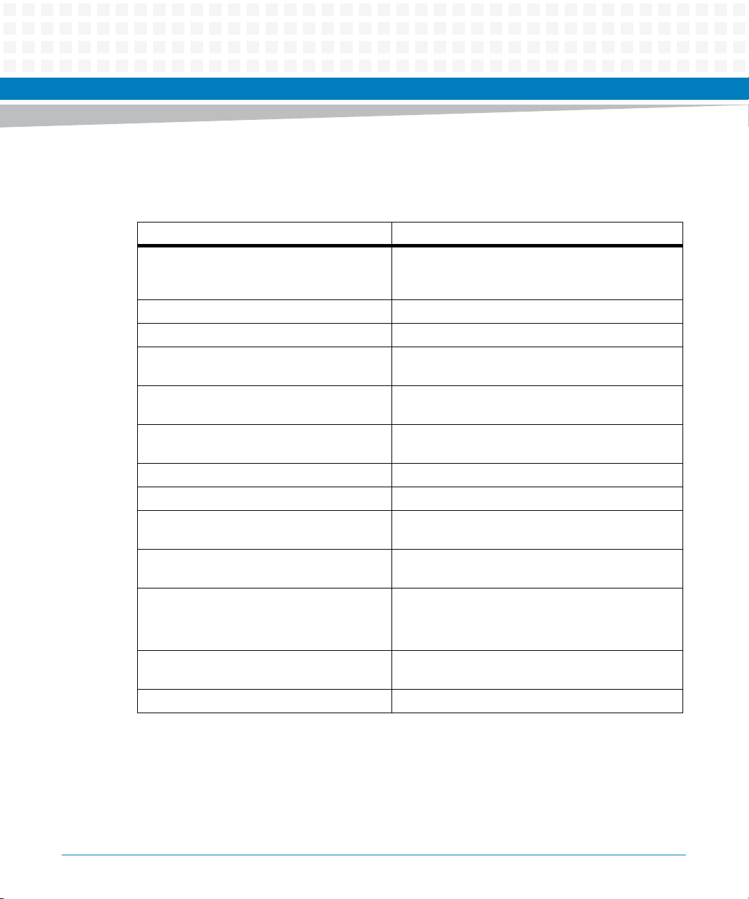
The following table describes the conventions used throughout this manual.
Notation Description
0x00000000 Typical notation for hexadecimal numbers (digits are
0b0000 Same for binary numbers (digits are 0 and 1)
bold Used to emphasize a word
Screen Used for on-screen output and code related elements
Courier + Bold Used to characterize user input and to separate it
Reference Used for references and for table and figure
About this Manual
0 through F), for example used for addresses and
offsets
or commands in body text
from system output
descriptions
File > Exit Notation for selecting a submenu
<text> Notation for variables and keys
[text] Notation for software buttons to click on the screen
and parameter description
... Repeated item for example node 1, node 2, ..., node
12
.
.
.
.. Ranges, for example: 0..4 means one of the integers
| Logical OR
MVME7616E Transition Module Installation and Use (6806800A43D)
Omission of information from example/command
that is not necessary at the time being
0,1,2,3, and 4 (used in registers)
11
Page 12
About this Manual
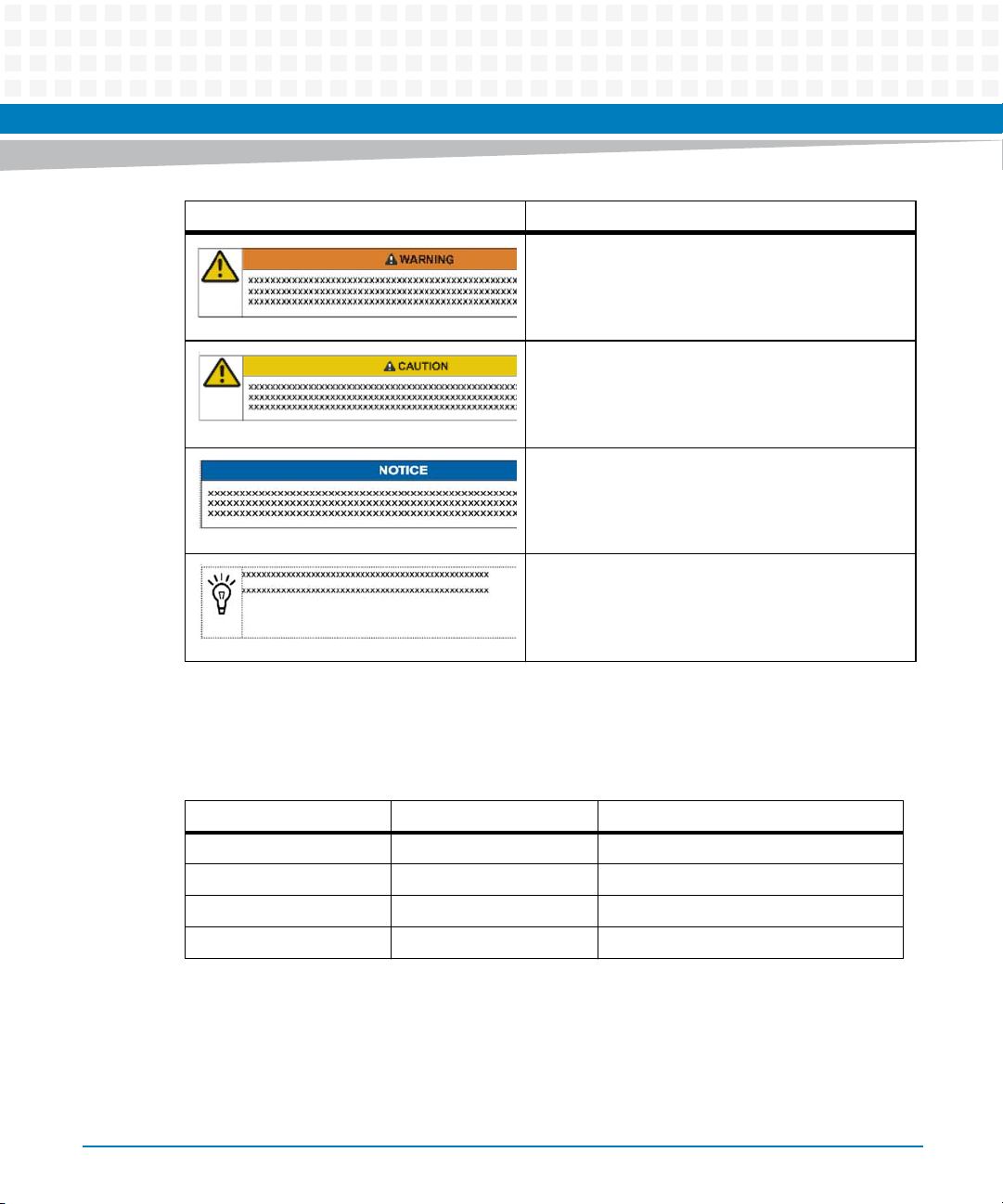
Notation Description
About this Manual
Indicates a hazardous situation which, if not avoided,
could result in death or serious injury
Indicates a hazardous situation which, if not avoided,
may result in minor or moderate injury
Indicates a property damage message
No danger encountered. Pay attention to important
information
Summary of Changes
This manual has been revised and replaces all prior editions.
Part Number Publication Date Description
6806800A43A June 2006 First edition
6806800A43B August 2008 Updated to Emerson style.
6806800A43C July 2009 Updated Table 1-6
6806800A43D April 2015 Re-branded to Artesyn template.
12
MVME7616E Transition Module Installation and Use (6806800A43D)
Page 13

General Information
1.1 Overview
This manual provides general information, hardware preparation, installation instructions, and
a functional description for the MVME761-001 and MVME761-011 Transition Modules.
The MVME761-0x1Transition Module provides the interface between the MVME5100 or
MVME5500
Single Board Computer VMEmodules and various peripheral devices. This module provides
industry standard connectors to simplify customer cable requirements for the serial port,
printer, and Ethernet signals.
1.2 Features
The features of the MVME761-0x1 Transition Module include:
Chapter 1
Industry-standard connectors for these interfaces:
– Two EIA-574 asynchronous serial ports (DTE)
– Two asynchronous/synchronous serial ports, configured for EIA-232-D (DCE or DTE)
– One parallel port (IEEE Standard 1284-I compliant)
– 10Base-T/100Base-TX Ethernet
Two 60-pin Serial Interface Module (SIM) connectors for configuring the
asynchronous/synchronous serial ports
Single-width board
Electro-Magnetic Interference (EMI) and Electro-Static Discharge (ESD) protection
1.3 General Description
The MVME761-0x1 Transition Module provides the interface between the standard Ethernet,
parallel port, and the serial port connectors on a variety of single board computers. All port I/O
controllers reside on the host VMEmodules. The MVME761 transition module Ethernet and
parallel port circuitry is passive. The serial port circuitry provides multiplexing and buffering
functions (refer to P2 Signal Multiplexing (P2MX) on page 29). The multiplexing function is
transparent to the user.
MVME7616E Transition Module Installation and Use (6806800A43D)
13
Page 14
General Information
Both MVME761-0x1 models use the same transition module. The MVME761-001 comes with
a P2 adapter that connects to a 3-row DIN chassis backplane. The MVME761-011 comes with a
P2 adapter that connects to a 5-row DIN chassis backplane.
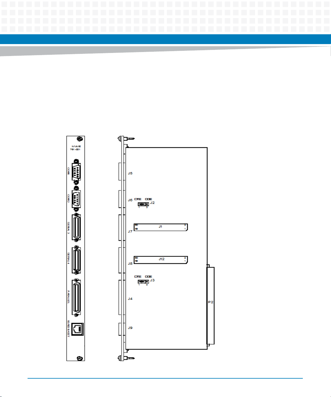
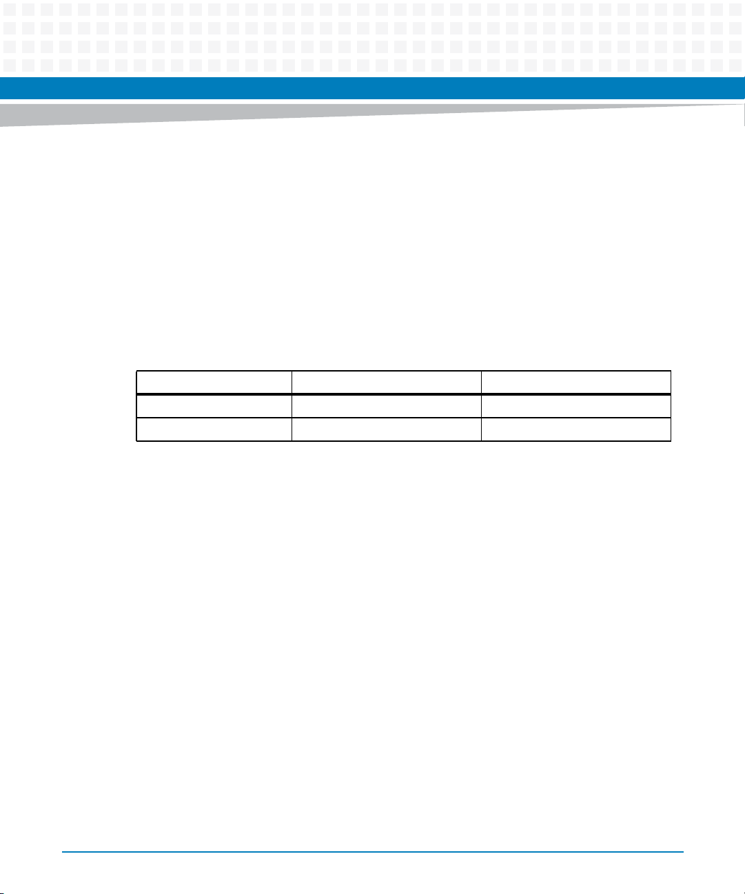
Figure 1-1 shows the MVME761 transition module component layout and the front panel. See
Table 1-2 for a list of the front panel port connectors.
Figure 1-1 RTM Front Panel and Components Side
14
MVME7616E Transition Module Installation and Use (6806800A43D)
Page 15
1.4 Serial Port Interface Modules
You may configure the asynchronous/synchronous serial ports (ports 3 and 4) to the
appropriate interface by installing a Serial Interface Module (SIM). A SIM is a small “plug-in”
printed circuit board that converts the TTL-level synchronous or asynchronous port signals to
industry standard voltage levels used by the ports. The SIM contains the receiver and
transmitter circuits for converting the input and output signals of the host VMEmodule to the
appropriate serial data communication protocol.
The SIMs for the MVME761 are listed in the following table.
Table 1-1 SIM Part Numbers
Interface Model Number Part Number
EIA-232-D DCE SIM232DCE5E 01-W3876B11A
EIA-232-D DTE SIM232DTE5E 01-W3877B11A
General Information
Additional SIMs may be released. Please see your Artesyn representative for a complete list of
SIMS that are available for the MVME761-0x1.
1.5 P2 Adapter Boards
The P2 adapters route the asynchronous and synchronous port, printer port, and Ethernet
signals to the MVME761 transition module.
MVME7616E Transition Module Installation and Use (6806800A43D)
15
Page 16
General Information
1.6 Three-row P2 Adapter (MVME761-001)
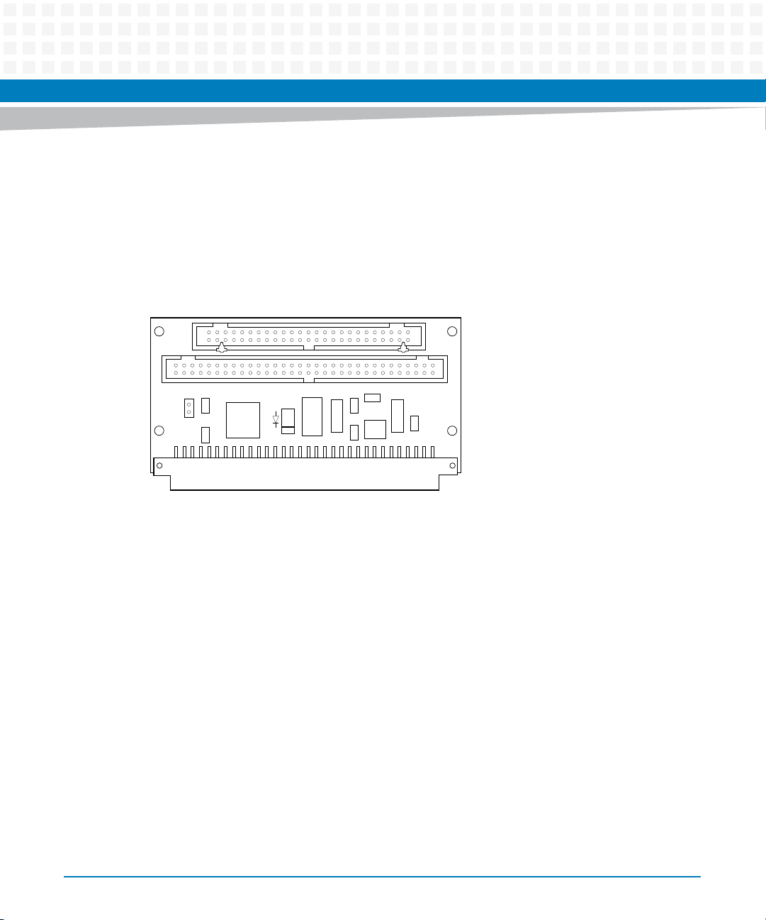
The P2 adapter for the MVME761-001 mounts onto a 3-row, 96-pin P2 backplane connector.
The 50-pin male connector, J2, carries the 8-bit SCSI signals from the host VMEmodules. To run
SCSI devices, you may install an additional transition module that is equipped with a SCSI port,
such as the MVME712B.
Figure 1-2 Three Row P2 Adapter
J2
2
1
J3
2
1
C5
C1
J1
1 32
C
B
A
1
R1
U1
9
CR1
25
17
P1
C3
C2
R2
C4
U2
50
49
64
63
C6
C7
++
C
B
A
1933 9610
This P2 adapter, and the cable for connecting to the MVME761 transition module, can be
ordered separately as model MVME761P2-001.
16
MVME7616E Transition Module Installation and Use (6806800A43D)
Page 17
General Information
1.7 Five-Row P2 Adapter (MVME761-011)
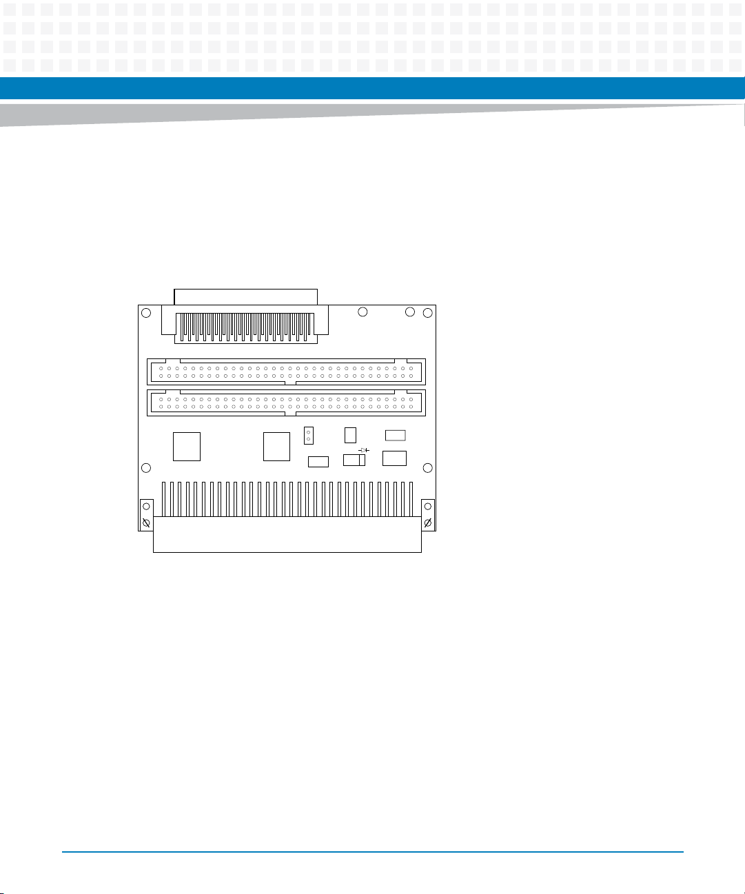
The P2 adapter for the MVME761-011 mounts onto a 5-row, 160-pin P2 backplane connector.
The 68- pin female connector, J1, carries 16-bit SCSI signals from the host VMEmodules. It also
has a 64-pin male connector, J3, for PMC I/O.
Figure 1-3 Five Row P2 Adapter
133
J3
2
1
2
1
J4
1
U1
9
1 32
D
C
B
A
Z
J1
25
17
1
9
J5
25
U2
17
P1
U3
C9
+
+
CR1
This P2 adapter, and the cable for connecting to the MVME761 transition module, can be
ordered separately as model MVME761P2-011.
1.8 Connectors and Cables
The connectors on the MVME761 transition module and the P2 adapters are listed in the
following tables. The port connectors are located on the front panel, which is shown in Figure
1-1. See Table 1-5 on page 19 for a list of the cables. See Chapter 4, Connector Pin Assignments.
64
63
64
63
C8
R4
D
C
B
A
Z
The cable used for connecting the MVME761 transition module to the P2 adapter is provided
with the MVME761-0x1
MVME7616E Transition Module Installation and Use (6806800A43D)
17
Page 18
General Information
1. You will need to purchase or fabricate the port cables.
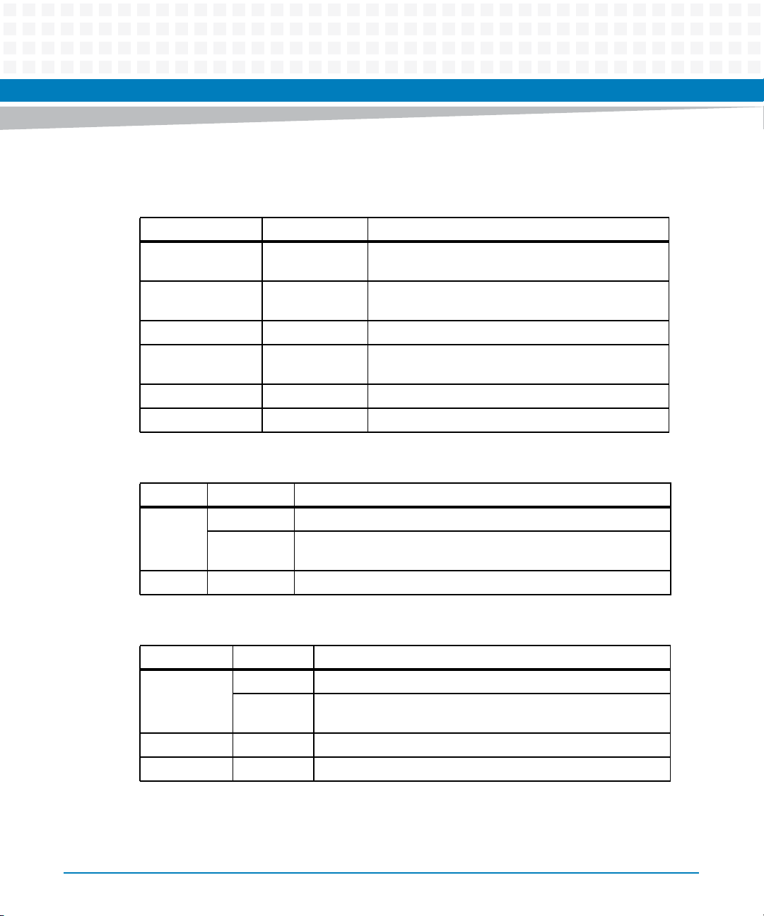
Table 1-2 MVME761 Transition Module Connectors
Type Number Description
COM1 and
COM2
Serial port 3
Serial port 4
Parallel port J4 36-pin female parallel port connector
10Base-T,
100Base-TX
SIM J1, J12 60-pin female connector
VME P2 64-pin male connector to J2 on the P2 adapter
J5
J6
J7
J8
J9 8-pin female RJ-45 Ethernet port connector
9-pin male DIN asynchronous serial port connector
26-pin female HD-26 synchronous serial port
connector
Table 1-3 3-Row P2 Adapter Connectors (MVME761-001)
Type Number Description
VME P1 96-pin female DIN 41612 connector to the chassis backplane
J3 64-pin male connector for output to P2 on the MVME761 transition
module
SCSI J2 50-pin male IDC connector for internal SCSI devices
Table 1-4 5-Row P2 Adapter Connectors (MVME761-011)
Type Number Description
18
VME P1 160-pin female DIN 41612 connector to the chassis backplane
J4 64-pin male connector for output to P2 on the MVME761
transition module
PMC I/O J3 64-pin male connector for PMC I/O
SCSI J1 68-pin female IDC connector for internal SCSI devices
MVME7616E Transition Module Installation and Use (6806800A43D)
Page 19
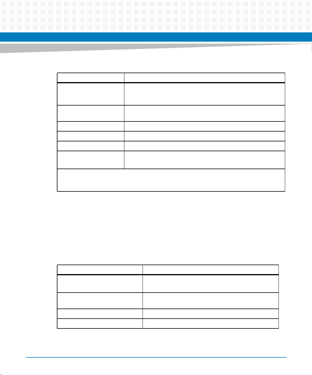
Table 1-5 Transition Module Cables
Part Number Description
General Information
Included with the
MVME761-0x1
User-supplied EIA-232-D DTE or DCE cable (pins used depend on the processor
User-supplied Centronics- type parallel printer cable, male-to-male
User-supplied 20-conductor cable; usually supplied with the modem
User-supplied 6-conductor cable; usually supplied with the modem
CBL761HD26DB25 Straight-through adapter cable with male HD-26 connector and female
If you supply your own 64-line cable to connect the P2 adapter to the MVME761 transition module, the
cable should not be longer than 1.5 feet. A longer cable is likely to cause problems, especially for the
Ethernet and parallel port signals.
1.9 Specifications
The MVME761 transition module specifications are shown in the next table.
64-line flat ribbon cable with 96-pin DIN connectors that connects P2
on the MVME761transition module to J3 on the 3-row P2 Adapter or J4
on the 5-row P2 adapter; 13 inches long. (30-W2799B02A).
VMEmodule)
DB-25 connector, 3 feet long. (30-NW9302B27)
Table 1-6 MVME761-0x1 Specifications
Characteristics Specifications
Power Requirements +12 Vdc, 100 mA typical, 200 mA maximum
-12 Vdc, 100 mA (for some of the SIMs)
o
Operating temperature 0
Storage temperature -40
Relative Humidity 5% to 90% (non-condensing)
MVME7616E Transition Module Installation and Use (6806800A43D)
to 55o C at chassis point of entry of forced air
(approximately 5 CFM)
o
to +85o C
19
Page 20

General Information
Table 1-6 MVME761-0x1 Specifications (continued)
Characteristics Specifications
Board Size
(excluding front panel)
1. J2 extends 1/4" further from the edge of the board.
Height: 9.187 inches(233.35 mm)
Height: 3.200 inches(80.00 mm)
Thickness: 0.063 inches (1.60 mm)
MVME761P26E-001: 1.85" deep, 3.75" high
MVME761026E-011: 2.725"
1.10 Cooling Requirements
The MVME761-0x1 is tested to operate under forced air cooling with an incoming air
temperature range of 0 degrees C to 55 degrees C. Adequate cooling can be achieved with air
flowing over the module at 5 cubic feet per minute. The exact amount of airflow required for
cooling depends on the ambient air temperature and the type, number, and location of
modules and other heat sources.
1
deep, 3.75" high
1.11 FCC Compliance
The MVME761-0x1 was tested in an FCC-compliant chassis, and meets the requirements for
Class A equipment. For minimum RF emissions, it is essential that you implement the following
conditions:
Install shielded cables on all external I/O ports
Connect conductive chassis rails to earth ground to provide a path for connecting shields
to earth ground
Tighten all front panel screws
20
MVME7616E Transition Module Installation and Use (6806800A43D)
Page 21
Hardware Preparation and Installation
2.1 Overview
This chapter provides unpacking instructions, hardware preparation, and installation
instructions for the MVME761 transition module, the P2 adapter, and the Serial Interface
Modules (SIMs).
2.2 Unpacking the Hardware
The MVME761 is packed in an antistatic wrapper to protect it from static discharge. Artesyn
strongly recommends that you use an antistatic wrist strap and a conductive foam pad when
handling the equipment. Electronic components can be extremely sensitive to electrostatic
discharge (ESD). After removing the board from the protective wrapper, place it component
side up on a grounded, static-free surface. Do not slide the board over any surface.
Unpack the equipment from the shipping carton. Refer to the packing list and verify that all the
items are present. Save the packing material for storing and reshipping of the equipment.
Chapter 2
2.3 Installing the Serial Interface Modules
Configure the serial ports 3 and 4 for the required interface by installing the appropriate SIM.
See Table 1-1 on page 15 for a list of the serial port interface types.
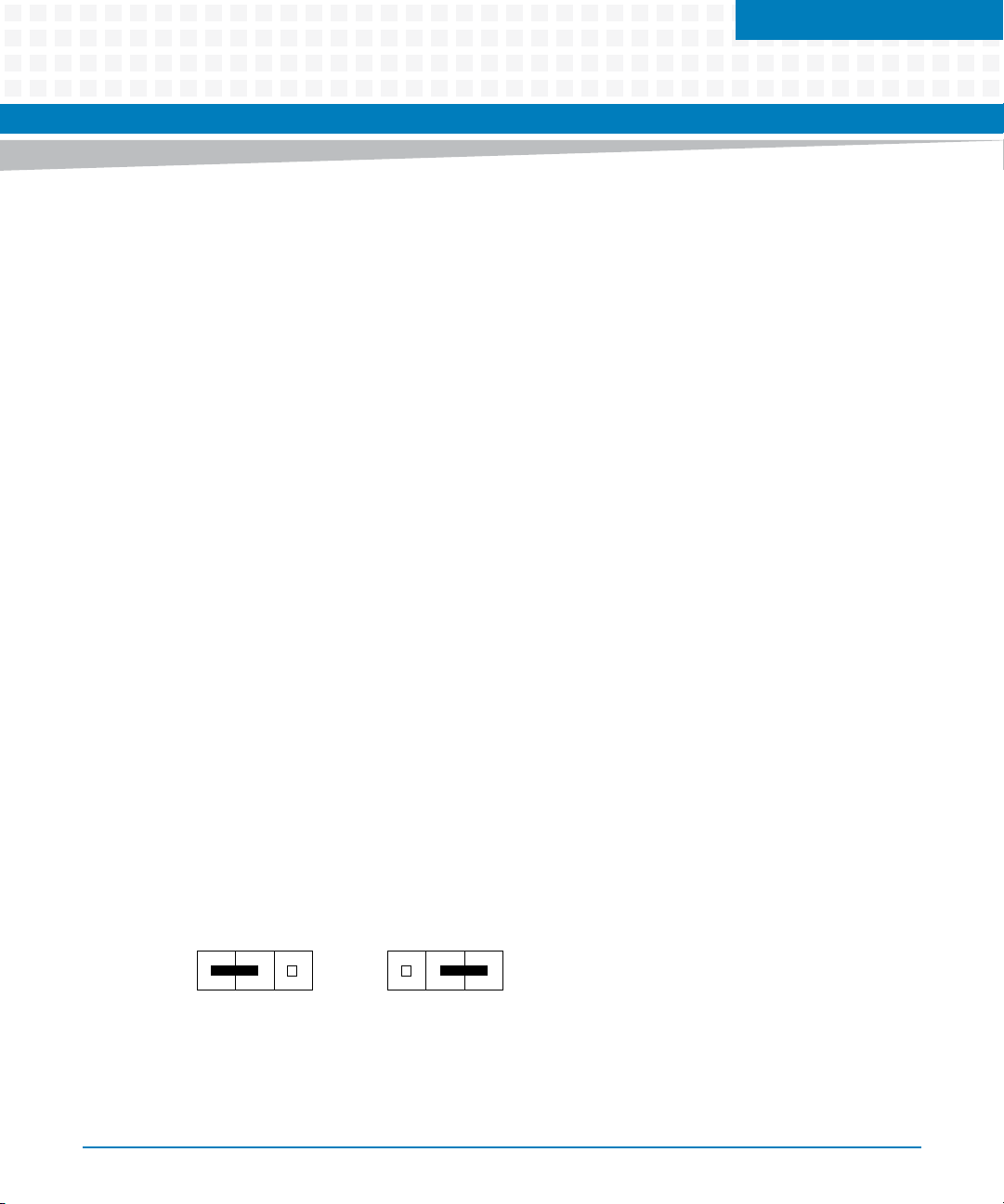
Prior to installing the SIMs, set the jumpers on header J2 (for serial port 3) and header J3 (for
serial port 4) for either DCE or DTE. Set the jumper to position:
1-2 if the SIM is for a DTE interface
2-3 if the SIM is for a DCE
Figure 2-1 Serial Port Interface Jumper Setting
123 123
DTE
MVME7616E Transition Module Installation and Use (6806800A43D)
DCE
21
Page 22
Hardware Preparation and Installation
You must set the jumpers and install the SIMs prior to installing the MVME761 transition
module in the system chassis.The SIMs plug into connector J1 (for serial port 3) or J12 (for serial
port 4) on the MVME761 transition module.
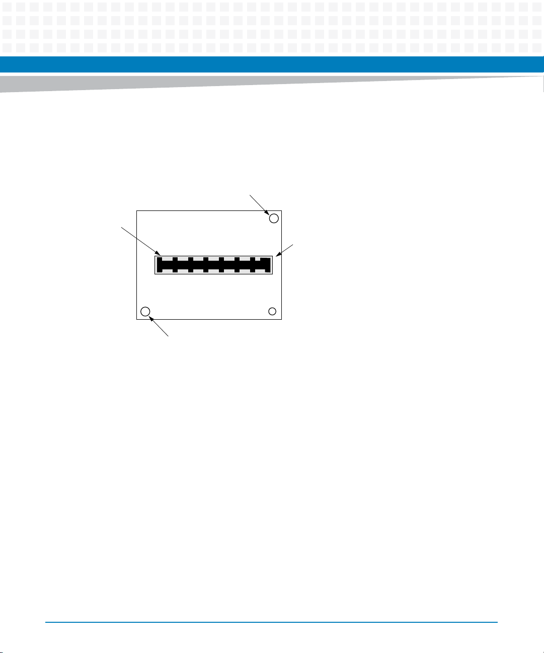
Figure 2-2 SIM Configuration
Mounting Hole
P1
Alignment
Key
22
Mounting Hole
11637 9610
Procedure
Install the SIMs on the MVME761 transition module per the following procedure:
1. Align the SIM so that P1 on the SIM lines up with the appropriate SIM connector (J1
for serial port 3 or J12 for serial port 4) on the transition module. Note the position
of the alignment key on P1. See Figure 2-2 on page 22.
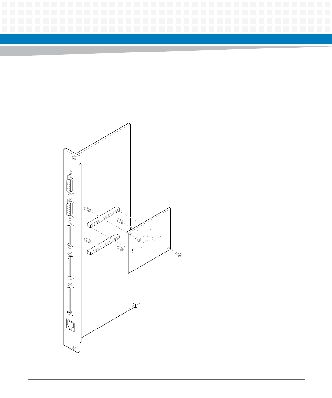
2. Place the SIM onto the transition module SIM connector, making sure that the
mounting holes also line up with the standoffs on the transition module as shown
in Figure 2-3 on page 23.
3. Gently press the top of the SIM to seat it on the transition module SIM connector. If
the SIM does not seat with gentle pressure, re-check the alignment of the
connectors.
MVME7616E Transition Module Installation and Use (6806800A43D)
Page 23
Hardware Preparation and Installation
Do not force the SIM onto the transition module.
4. Secure the SIM to the transition module standoffs with the two Phillips-head
screws provided. Do not over tighten the screws.
Figure 2-3 Installing the SIM
1911 9609
MVME7616E Transition Module Installation and Use (6806800A43D)
23
Page 24
Hardware Preparation and Installation
2.4 Installing the Transition Module and P2 Adapter
Install the MVME761 transition module and P2 adapter in the system chassis. The P2 adapter is
required because the P2 connector on the transition module is not compatible with the P2
connector on the chassis backplane.
ESD
Artesyn strongly recommends that you use an antistatic wrist strap and a conductive foam pad
when installing or upgrading a system. Electronic components, such as disk drives, computer
boards, and memory modules, can be extremely sensitive to electrostatic discharge (ESD).
After removing the component from its protective wrapper or from the system, place the
component flat on a grounded, static-free sur face (and, in the case of a board, component side
up). Do not slide the component over any surface.
If an ESD station is not available, you can avoid damage resulting from ESD by wearing an
antistatic wrist strap (available at electronics stores) that is attached to an active electrical
ground. Note that a system chassis may not be grounded if it is unplugged.
Install the MVME761-0x1 in the system chassis according to the procedures in this chapter.
An MVME5100/MVME5500 module that is designed for use with an MVME712M Transition
Module will be damaged if you use it with an MVME761-0x1 Transition Module.
Connecting modules while power is applied may result in damage to components on the
module.
24
Dangerous voltages, capable of causing death, are present in this equipment. use extreme
caution when handling, testing, and adjusting.
MVME7616E Transition Module Installation and Use (6806800A43D)
Page 25
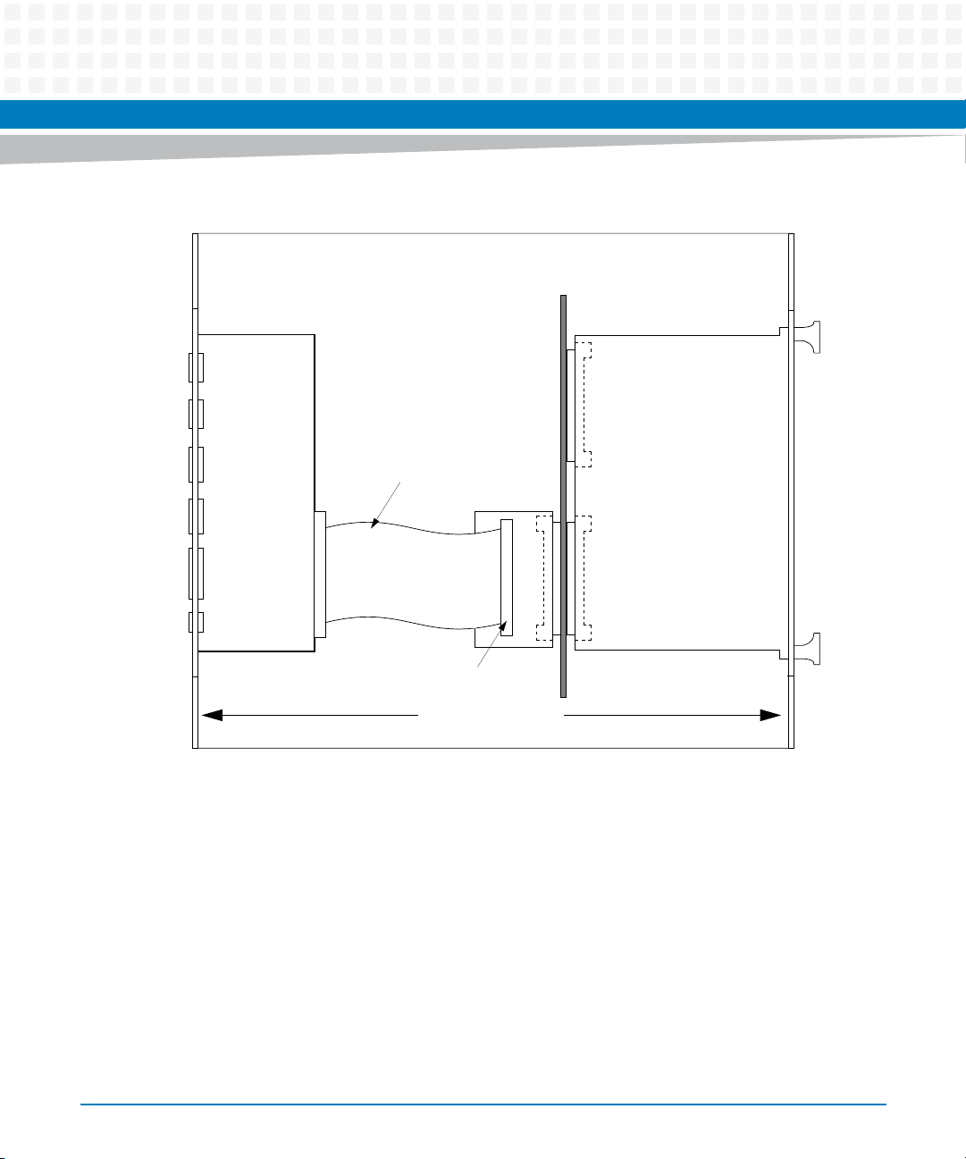
Figure 2-4 Chassis Connections
Hardware Preparation and Installation
VME BACKPLANE
MVME761 Transition Module
P2
30-W2799B02A
64-CONDUCTOR
J3 ON THE 3-ROW P2 ADAPTER
J4 ON THE 5-ROW P2 ADAPTER
ENCLOSURE BOUNDARY
P2 ADAPTER
Host Board
P1
P1
P2
11654.00 9610
Procedure
Follow these steps to configure, install, and cable the transition module.
1. Turn all equipment power OFF and disconnect the power cable from the AC power
source.
2. Remove the chassis cover per the instructions in the equipment user's manual.
3. If the chassis has a rear card cage, remove the filler panel(s) from the appropriate
card slot(s) at the rear of the chassis.
MVME7616E Transition Module Installation and Use (6806800A43D)
25
Page 26

Hardware Preparation and Installation
4. If necessary, move some of the other modules to allow space for the cables
connected to the P2 adapter and the transition module.
5. Install the jumper on header J1 (on the 3-row P2 adapter or header J5 on the 5-row
P2 adapter) if you are supporting SCSI devices.
6. Attach the P2 adapter, for either the 3-row or 5-row version, to the backplane
connector that is directly in line with the P2 connector on the host VMEmodule.
7. Orient pin 1 of the P2 adapter’s connector with pin 1 of the backplane connector.
8. Attach the 64-conductor cable (furnished with the MVME761-0x1) to the P2
adapter (J3 on the 3-row version, J4 on the 5-row version). Be sure to orient cable
pin 1 with connector pin 1.
9. Attach the 64-conductor cable to connector P2 on the transition module. Be sure
to orient cable pin 1 with connector pin 1.
10.Insert the transition module into the chassis slot, and tighten the attaching screws.
Make sure there is good contact with the transverse mounting rails in order to
minimize RF emissions.
11.Install the chassis cover, making sure that cables are not pinched by the cover.
12.Connect the power cable to the AC power source.
26
MVME7616E Transition Module Installation and Use (6806800A43D)
Page 27

Functional Description
3.1 Overview
This chapter provides information on MVME761 transition module and SIM circuitry, P2 signal
multiplexing, and the configuration of the serial ports.
3.2 Circuitry
The MVME761 transition module and the Serial Interface Modules (SIMs) convert the TTL level
signals to and from the MVME5100, and MVME5500 modules to the reception and
transmission levels specified by the appropriate port interface standard.
The MVME761 transition module contains a small amount of “house keeping” circuitry. Bulk
capacitors are on the power sources (+5Vdc, +12Vdc, and -12Vdc). Pull-up resistors put the
inputs to the host board in a known high even when no SIM is installed.
Chapter 3
MVME7616E Transition Module Installation and Use (6806800A43D)
27
Page 28
Functional Description
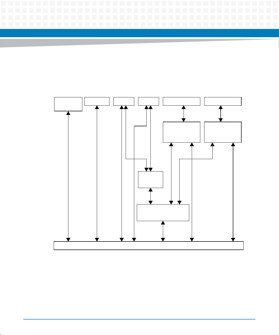
The block diagram for the MVME761 transition module is shown in Figure 3-1. The block
diagram for the 3-row DIN backplane P2 adapter is shown in Figure 3-2. The block diagram for
the 5-row DIN backplane P2 adapter is shown in Figure 3-3.
Figure 3-1 Transition Module Block Diagram
10Base-T COM1
100Base-TX
COM2
Serial Interface
Buffers
EIA-232-D
P2 Multiplex Function
64-Pin DIN Connector
Serial 3
Module (SIM)
Serial 4Parallel
Serial Interface
Module (SIM)
28
11638.00 9611
MVME7616E Transition Module Installation and Use (6806800A43D)
Page 29
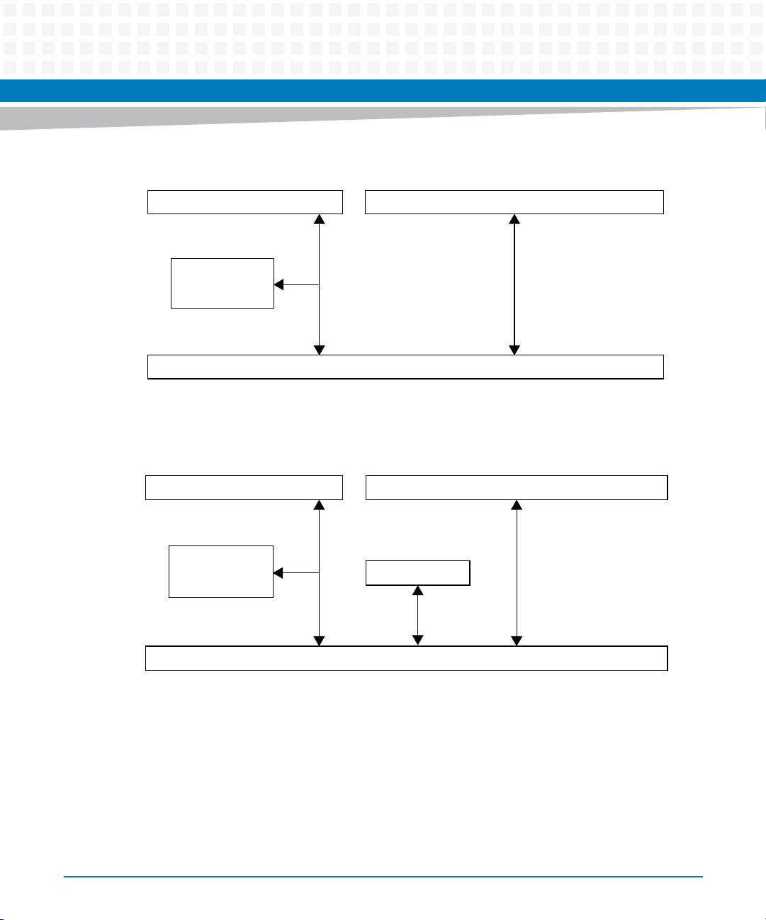
Figure 3-2 3-Row DIN Backplane P2 Adapter Block Diagram
Functional Description
8-bit Single-ended SCSI
SCSI
Terminators
3-Row Backplane Connector
64-pin Connector to MVME761 Transition Module
Figure 3-3 5-Row DIN Backplane P2 Adapter Block Diagram
16-bit Single-ended SCSI
SCSI
Terminators
64-pin Connector to MVME761 Transition Module
PMC I/O
11639.00 9611
5-Row Backplane Connector
3.3 P2 Signal Multiplexing (P2MX)
Because of a limited number of pins on the P2 connector, both the VME processor board and
the MVME761 transition module multiplex and demultiplex some of the P2 signals. This
function, called P2MX is transparent to the software and the user.
MVME7616E Transition Module Installation and Use (6806800A43D)
11752.00 9703
29
Page 30

Functional Description
Four pins are used for the signal multiplexing:
MXCLK
MXSYNC#
MXDO
MXDI
30
MVME7616E Transition Module Installation and Use (6806800A43D)
Page 31
Functional Description
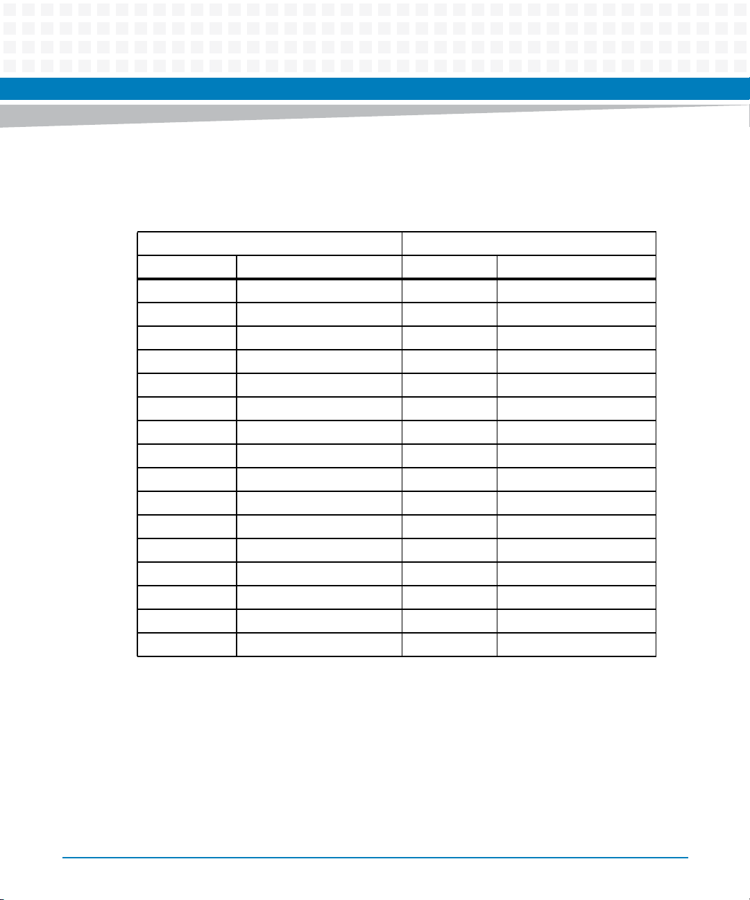
Sixteen time slots are defined and allocated. The signal multiplexing sequences are listed in the
following table.
Table 3-1 P2 signal multiplexing sequence
MXDO (from the MVME510x/MVME550x) MXDI (from the MVME7616E)
Time Slot Signal Name Time Slot Signal Name
0RTS3 0CTS3
1 DTR3 1 DSR3/MID1
2 LLB3/MODSEL 2 DCD3
3 RLB3 3 TM3/MID0
4 RTS4 4 RI3
5 DTR4 5 CTS4
6 LLB4 6 DSR4/MID3
7 RLB4 7 DCD4
8 IDREQ# 8 TM4/MID2
9 DTR1 9 RI4
10 DTR2 10 RI1
11 Reserved 11 DSR1
12 Reserved 12 DCD1
13 Reserved 13 RI2
14 Reserved 14 DSR2
15 Reserved 15 DCD2
MXCLK is the 10MHz bit clock for the time-multiplexed data lines, MXDO and MXDI.
MXSYNC# is asserted for one bit time at Time Slot 15 by the MVME5100 and MVME5500
MXSYNC# is used by the MVME761 transition module to synchronize with the VME
modules.
MXDO is the time-multiplexed output line from the main board and MXDI is the time-
multiplexed line from the MVME761 transition module. A 16-to-1 multiplexing scheme is
used with a 10MHz bit rate.
MVME7616E Transition Module Installation and Use (6806800A43D)
31
Page 32
Functional Description
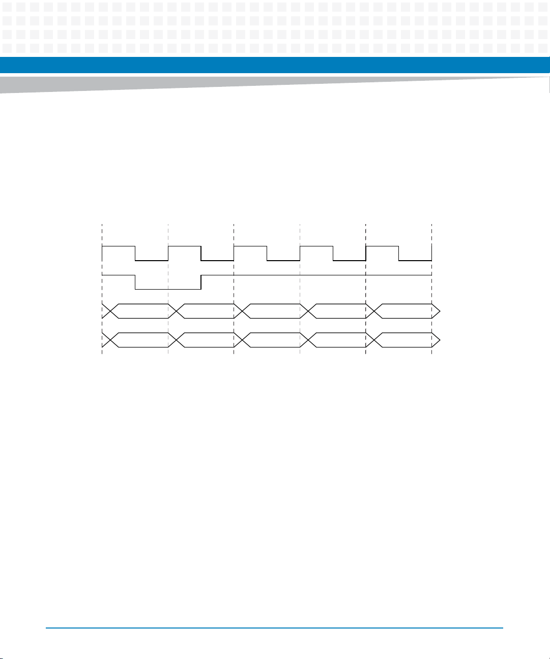
MXSYNC# is clocked out using the falling edge of MXCLK and MDXO is clocked out with the
rising edge of the MXCLK. MXDI is sampled at the rising edge of MXCLK (the transition module
synchronizes MXDI with MXCLK’s rising edge).
The timing relationships among MXCLK, MXSYNC#, MXDO, and MXDI are illustrated in the
next figure.
Figure 3-4 Multiplex Signal Timing Chart
Time Slot 1 Time Slot 2
MXCLK
MXSYNC#
MXDO
MXDI
Time Slot 15 Time Slot 0
RTS3 DTR3 LLB3 RLB3Reserved
CTS3 DSR3 DCD3 TM3DCD2
3.4 Serial Interface Module Circuitry
Each Serial Interface Module has a 60-pin connector that provides all signal and power
connections to the MVME761 transition module.
TTL-level signals
All TTL-level signals, with the exception of data and clocks, are active low. The pullup resistors
on the MVME761 transition module drive all TTL inputs to the SIM to a known logic level.
SIMs
The SIMs have surge suppression circuitry for all port signals going to the external connector.
This consists of a series resistor and a dual 15V clamp diode to chassis ground. All series
resistors are 100 ohms except on the EIA-530 balanced drives, which use 10 ohm series
resistors.
Time Slot 3
11640.00 9611
32
MVME7616E Transition Module Installation and Use (6806800A43D)
Page 33

Functional Description
EIA-232-D SIMs employ MC145406 ICs as line transmitters to convert the TTL output signals
from the host VMEmodule to EIA-232-D voltage levels. As line receivers, the MC145406 ICs
convert the EIA-232-D input signals to TTL voltage levels which are sent to the VME module.
The MC145406 transceiver IC requires a series diode on the +12V supply and a clamp diode to
logic ground on the -12V supply. The diodes are located on the transition module rather than
on the SIM due to space limitations.
For all port interfaces, the SIMs support the transmitter signal element timing as either input or
output signals.
MVME7616E Transition Module Installation and Use (6806800A43D)
33
Page 34

Functional Description
3.5 COM1 and COM2 Asynchronous Serial Ports
The asynchronous serial port (COM1 and COM2) configuration is shown in the next figures.
34
MVME7616E Transition Module Installation and Use (6806800A43D)
Page 35
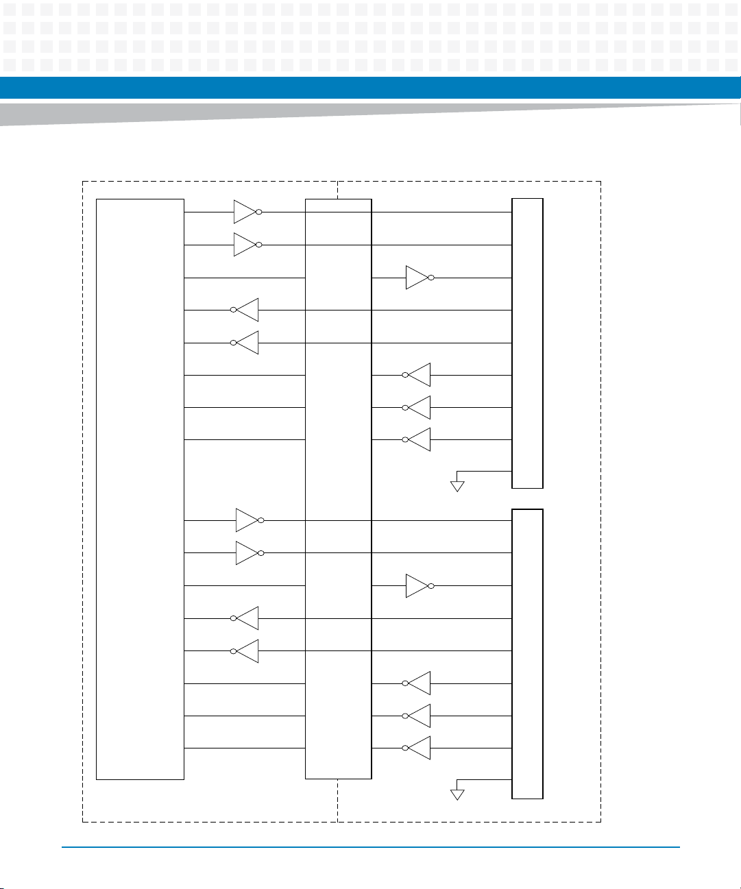
Figure 3-5 EIA-574 DTE Port Configuration
SOUT1
Functional Description
DB9
TXD
3
RTS1#
DTR1#
SIN1
CTS1#
DSR1#
DCD1#
RI1#
PC87308
SOUT2
RTS2#
DTR2#
SIN2
CTS2#
DSR2#
P2/P2MX
GND
RTS
DTR
RXD
CTS
DSR
DCD
TXD
RTS
DTR
RXD
CTS
DSR
7
4
2
COM1
8
6
1
RI
9
5
DB9
3
7
4
2
COM2
8
6
DCD2#
RI2#
VME Module MVME761
Transition Module
MVME7616E Transition Module Installation and Use (6806800A43D)
GND
DCD
1
RI
9
5
35
Page 36

Functional Description
3.6 Asynchronous/Synchronous Serial Ports
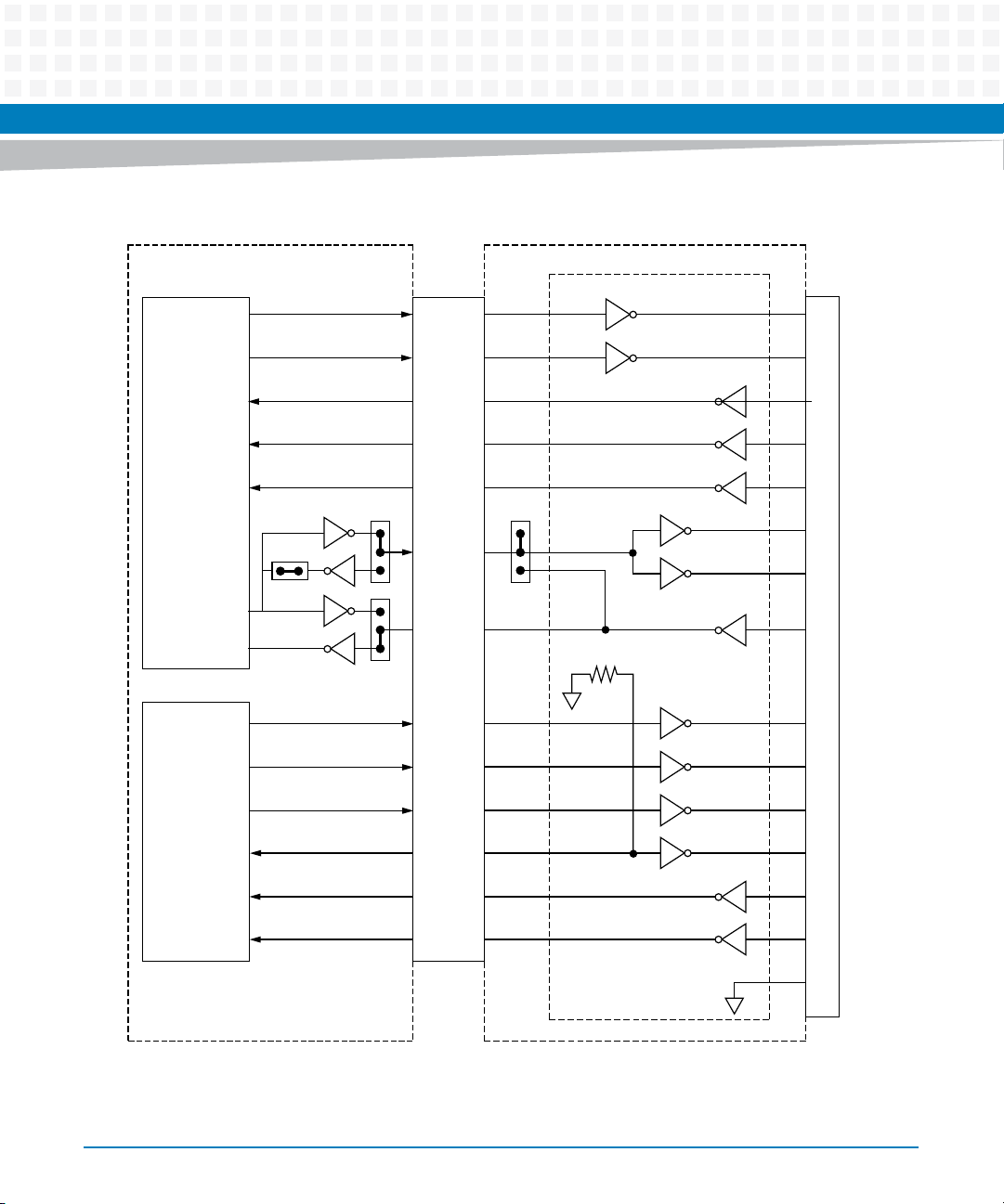
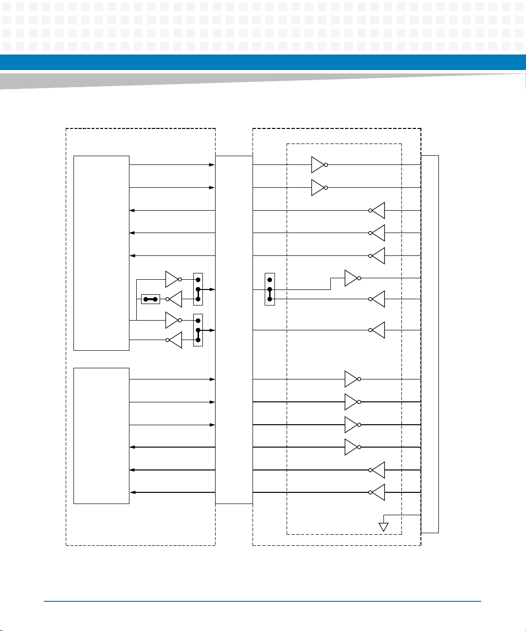
The asynchronous/synchronous serial port (Port 3 and Port 4) interface configuration
diagrams are on the following pages.
36
MVME7616E Transition Module Installation and Use (6806800A43D)
Page 37
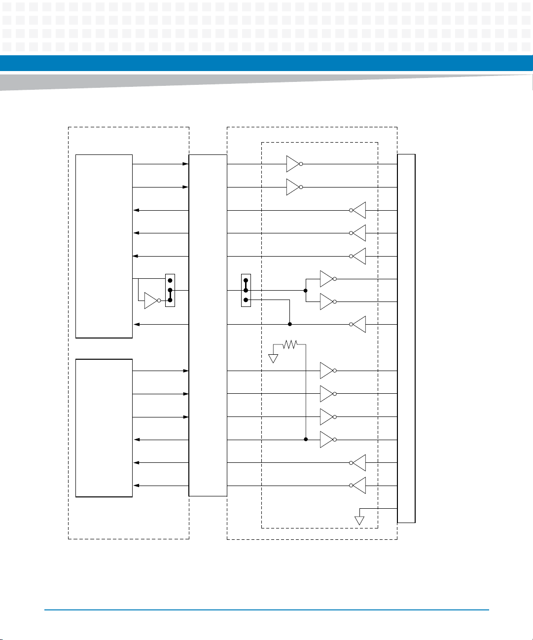
Figure 3-6 EIA232-DCE Configuration Port 3
Functional Description
DCE
VME MODULE
Z85230 SCC
TXD
RTS#
RXD
CTS#
DCD#
TRXC
RTXC
Z8536 CIO
DTR#
LLB#
RLB#
J18
3
2
1
P2/P2MX
MVME761
EIA232-DCE SIM
J2
3
2
1
HD26
3
5
2
4
20
15
17
24
8
25
22
DSR#
RI#
TM#
Header J18 1-2 Header J2 2-3
MVME7616E Transition Module Installation and Use (6806800A43D)
6
21
18
7
37
Page 38
Functional Description
Figure 3-7 EIA232-DCE Configuration Port 4
DCE
Z85230 SCC
TXD
RTS#
RXD
CTS#
DCD#
TRXC
RTXC
Z8536 CIO
DTR#
LLB#
VME MODULE
J19
J16
1
2
3
1
2
3
P2/P2MX
MVME761
EIA232-DCE SIM
J3J17
3
2
1
HD26
3
5
2
4
20
15
17
24
8
25
RLB#
DSR#
RI#
TM#
Headers: J16 2-3 Header J3 2-3
J17 1-2
J19 1-2
38
MVME7616E Transition Module Installation and Use (6806800A43D)
22
6
21
18
7
Page 39
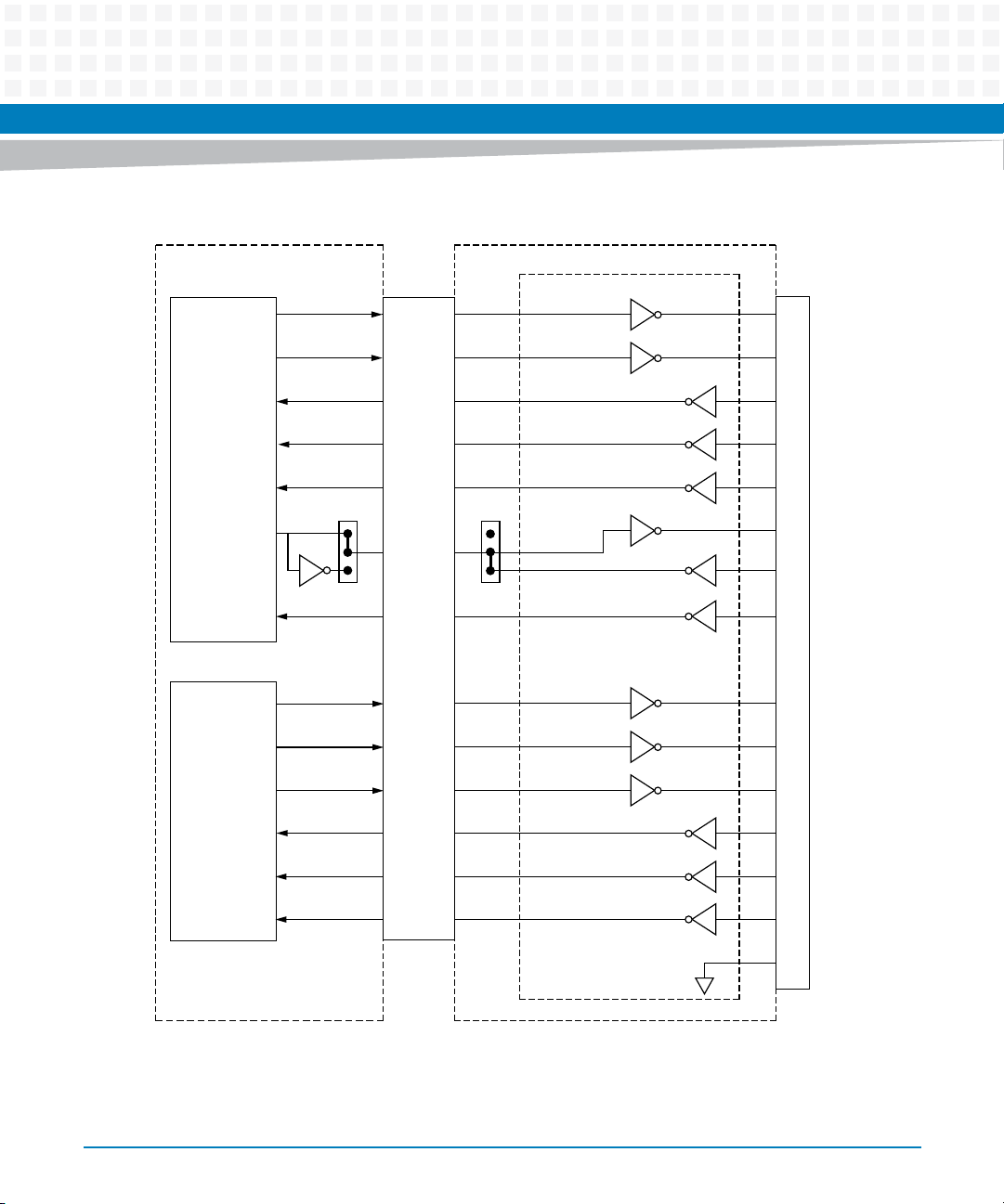
Figure 3-8 EIA232-DTE Configuration Port 3
Functional Description
DTE
VME MODULE
Z85230 SCC
RTS#
CTS#
DCD#
TRXC
RTXC
Z8536 CIO
DTR#
LLB#
RLB#
TXD
RXD
J18
3
2
1
P2/P2MX
MVME761
EIA232-DTE SIM
J2
3
2
1
HD26
2
4
3
5
8
24
15
17
20
18
21
DSR#
RI#
TM#
Header J18 2-3 Header J2 1-2
MVME7616E Transition Module Installation and Use (6806800A43D)
6
22
25
7
39
Page 40
Functional Description
Figure 3-9 EIA232-DTE Configuration Port 4
DTE
Z85230 SCC
TXD
RTS#
RXD
CTS#
DCD#
TRXC
RTXC
Z8536 CIO
DTR#
LLB#
VME MODULE
J19
J16
1
2
3
1
2
3
P2/P2MX
MVME761
EIA232-DTE SIM
J3J17
3
2
1
HD26
2
4
3
5
8
24
15
17
20
18
Headers: J16 2-3
40
RLB#
DSR#
RI#
TM#
J17 2-3
21
6
22
25
7
Header J3 1-2
MVME7616E Transition Module Installation and Use (6806800A43D)
Page 41
Connector Pin Assignments
4.1 Overview
This chapter provides the pin assignments for the P2 connector and front panel port
connectors on the MVME761 transition module, as well as for the SCSI and PMC I/O connectors
on the P2 adapters.
4.2 P2 Connector
Signaling and power from the host VMEmodules are received through connector P2, a 64-pin
DIN connector. Because the P2 adapter reroutes some of the signals, connector P2 on the
MVME761 transition module is not pin-for-pin compatible with connector P2 on the host
VMEmodules.
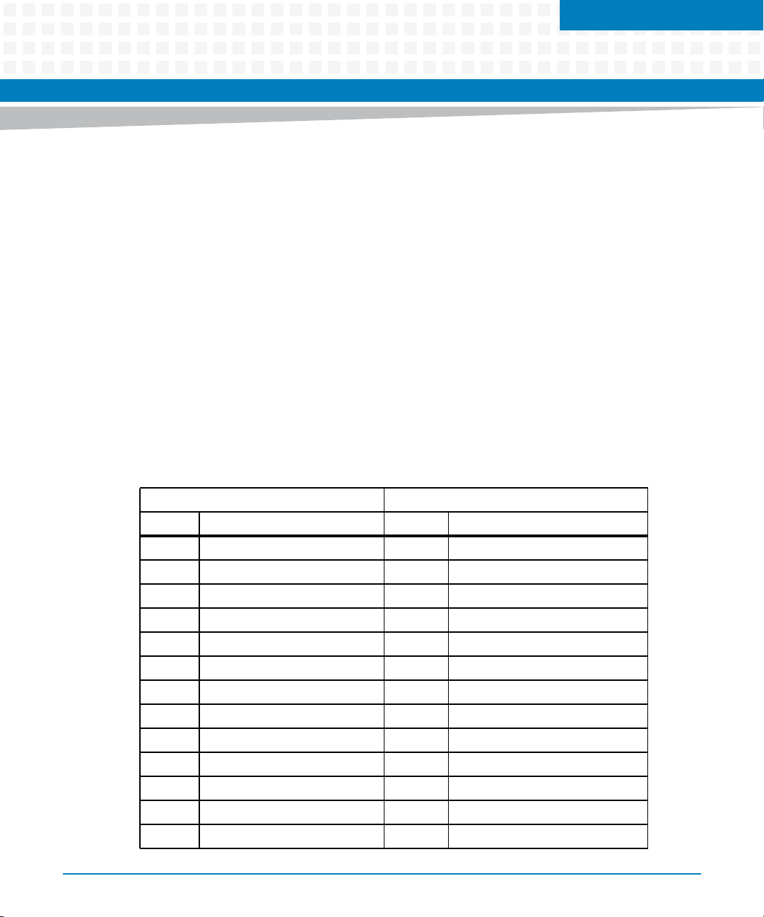
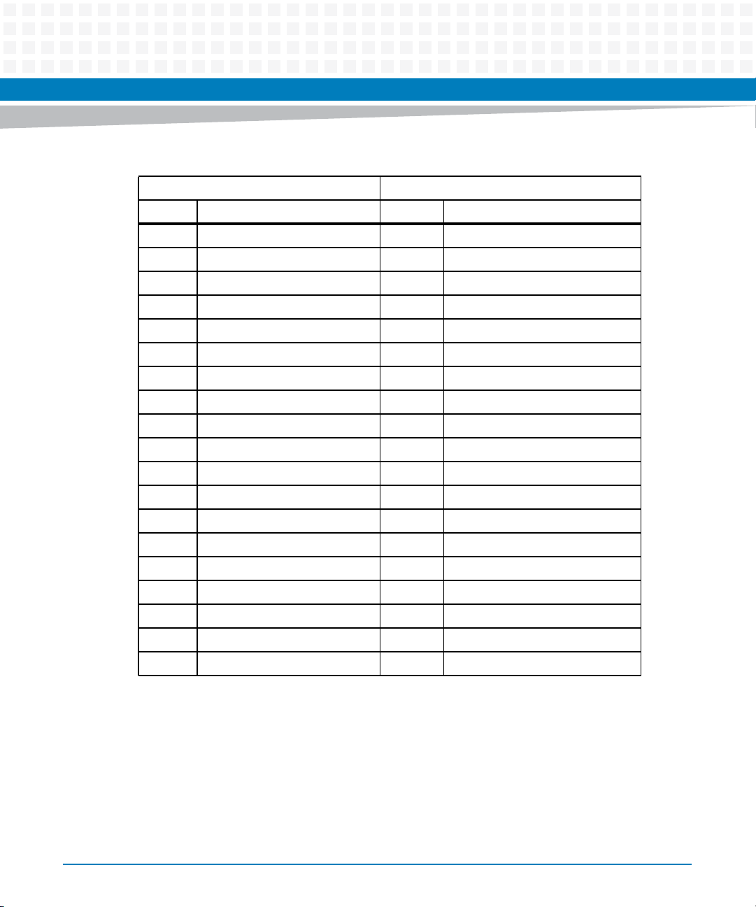
The pin assignments and signal mnemonics for the MVME761 transition module P2 connector
are listed in the following table.
Chapter 4
Table 4-1 P2 Connector Pin Assignments
Row A Pins Row C Pins
Pin Signal Pin Signal
1 C- (R- for RJ-45 J9) 1 C+ (R+ for RJ-45 J9)
2T- 2 T+
3R- 3 R+
4 +12VF 4 PRSTB#
5 GND 5 PRD0
6 PRD1 6 PRD2
7 PRD3 7 PRD4
8 PRD5 8 PRD6
9 PRD7 9 GND
10 PRACK# 10 GND
11 PRBSY 11 PRPE
12 PRSEL 12 INPRIME#
13 PRFAULT# 13 GND
MVME7616E Transition Module Installation and Use (6806800A43D)
41
Page 42
Connector Pin Assignments
Table 4-1 P2 Connector Pin Assignments (continued)
Row A Pins Row C Pins
Pin Signal Pin Signal
14 AUTOFD# 14 GND
15 SELIN# 15 GND
16 TXD3 16 RXD3
17 RTXC3 17 TRXC3
18 GND 18 TXD1_232
19 GND 19 RXD1_232
20 GND 20 RTS1_232
21 CTS1 21 GND
22 TXD4 22 GND
23 RXD4 23 GND
42
24 RTXC4 24 GND
25 TRXC4 25 GND
26 No Connect 26 -12VF
27 MSYNC# 27 GND
28 MCLK 28 GND
29 TXD2_232 29 GND
30 RXD2_232 30 GND
31 RTS2_232 31 CTS2_232
32 MDO 32 MDI
MVME7616E Transition Module Installation and Use (6806800A43D)
Page 43
Connector Pin Assignments
4.3 Asynchronous Serial Port Connectors (J5/J6)
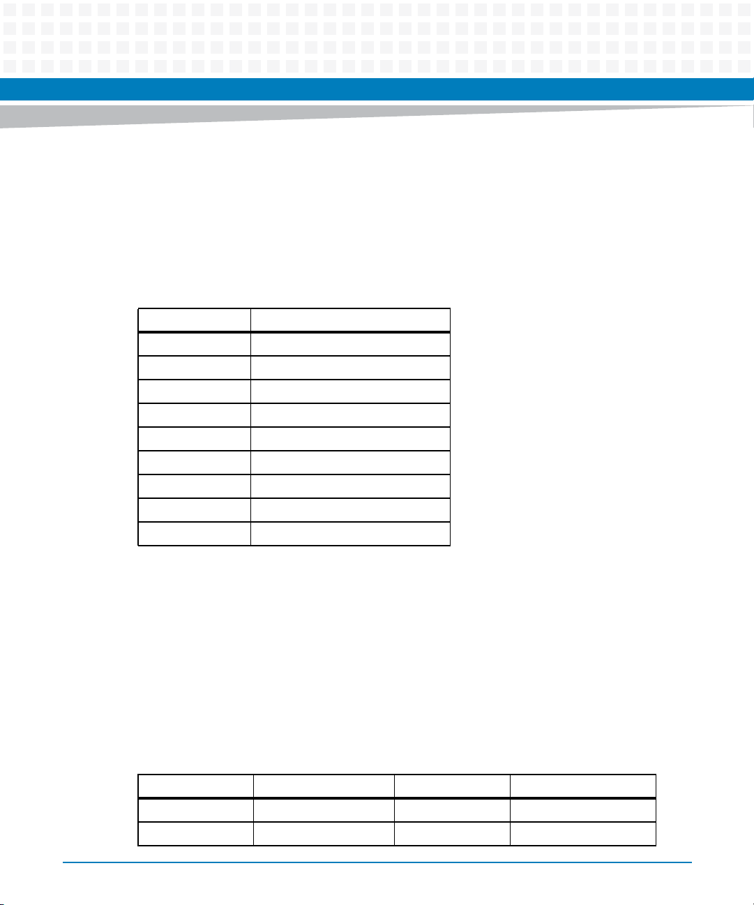
The interface for the asynchronous serial ports, COM1 and COM2, is provided with two
standard DB9 connectors, J5 and J6. The connector shields for these ports are tied to chassis
ground. The pin assignments and signal mnemonics for these connectors are listed in Table
4-2.
Table 4-2 COM1 and COM2 Pin Assignments
Pin Signal
1 DCD
2 RXD
3 TXD
4DTR
5GND
6DSR
7RTS
8CTS
9RI
4.4 Asynchronous/Synchronous serial Port connectors (J7/J8)
The interface for the asynchronous/synchronous serial ports 3 and 4 is provided by two HD-26
connectors, J7 and J8. The connector shields for these ports are tied to chassis ground.
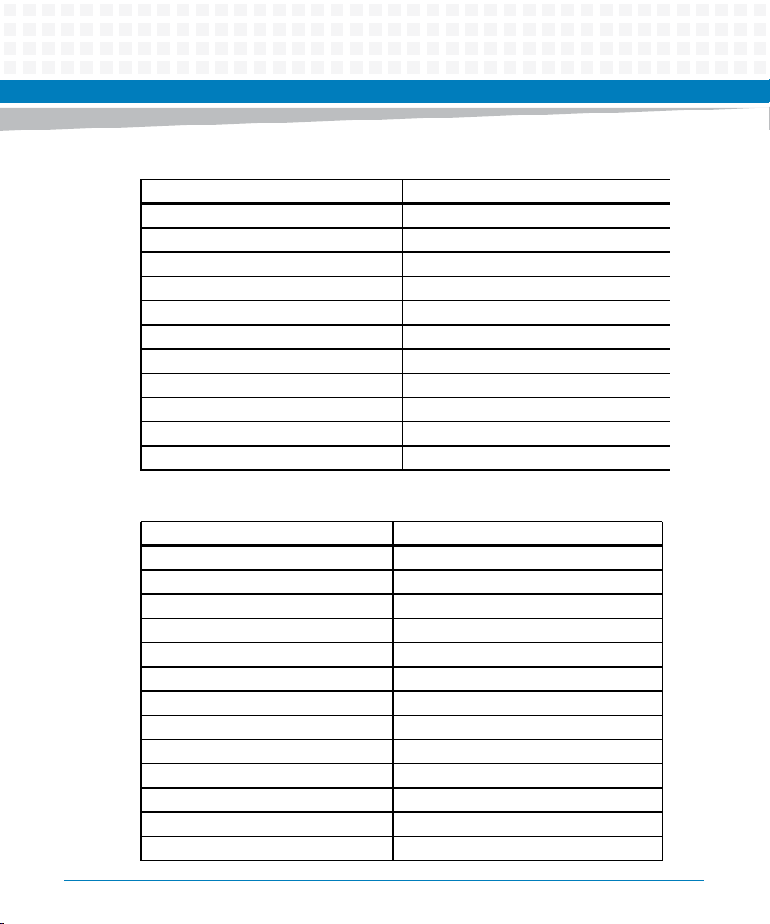
The pin assignments and signal mnemonics for serial ports 3 and 4 are listed in the following
tables.
Table 4-3 Serial Port 3 Pin Assignments
Pin Signal Pin Signal
1 No Connect 14 SP3_P14
2 TXD3 15 TXCI3
MVME7616E Transition Module Installation and Use (6806800A43D)
43
Page 44
Connector Pin Assignments
Table 4-3 Serial Port 3 Pin Assignments (continued)
Pin Signal Pin Signal
3 RXD3 16 SP3_P16
4 RTS3 17 RXCI3
5 CTS3 18 LLB3
6 DSR3 19 SP3_P19
7 GND 20 DTR3
8 DCD3 21 RLB3
9 SP3_P9 22 RI3
10 SP3_P10 23 SP3_P23
11 SP3_P11 24 TXCO3
12 SP3_P12 25 TM3
13 SP3_P13 26 No Connect
44
Table 4-4 Serial Port 4 Pin Assignments
Pin Signal Pin Signal
1 No Connect 14 SP4_P14
2 TXD4 15 TXCI4
3 RXD4 16 SP4_P16
4 RTS4 17 RXCI4
5 CTS4 18 LLB4
6 DSR4 19 SP4_P19
7 GND 20 DTR4
8 DCD4 21 RLB4
9 SP4_P9 22 RI4
10 SP4_P10 23 SP4_P23
11 SP4_P11 24 TXCO4
12 SP4_P12 25 TM4
13 SP4_P13 26 No Connect
MVME7616E Transition Module Installation and Use (6806800A43D)
Page 45
4.5 Parallel I/O Port Connector (J4)
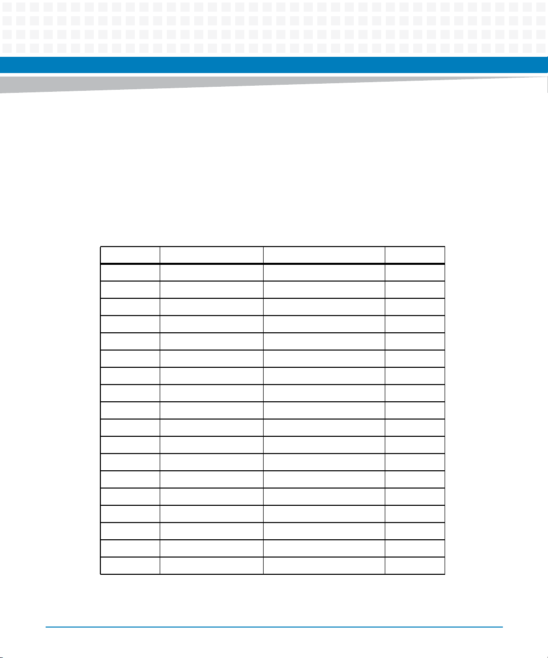
The interface for the parallel port is a standard IEEE P1284-C, 36-pin connector, J4. The
functionality of each signal depends on the mode of operation of this bidirectional Parallel
Peripheral Interface. Refer to the IEEE P1284 D2.00 Standard for a complete description of each
signal function. The connector shield is tied to chassis ground.
The pin assignments and signal mnemonics for this connector are listed in Table 4-5.
Table 4-5 Parallel I/O Connector Pin Assignments
Pin Signal Signal Pin
1 PRBSY GND 19
2 PRSEL GND 20
3 PRACK_ GND 21
4 PRFAULT_ GND 22
Connector Pin Assignments
5 PRPE GND 23
6 PRD0 GND 24
7 PRD1 GND 25
8 PRD2 GND 26
9 PRD3 GND 27
10 PRD4 GND 28
11 PRD5 GND 29
12 PRD6 GND 30
13 PRD7 GND 31
14 INPRIME_ GND 32
15 PRSTB_ GND 33
16 SELIN_ GND 34
17 AUTOFD_ GND 35
18 Pull-up No Connect 36
MVME7616E Transition Module Installation and Use (6806800A43D)
45
Page 46
Connector Pin Assignments
4.6 Ethernet Connector (J9)
The 10Base-T/100Base-TX Ethernet interface is a RJ-45 connector, J9. The connector shield is
tied to chassis ground. The pin assignments and signal mnemonics for this connector are listed
in Table 4-6.
Table 4-6 10Base-T/100Base-TX Pin Assignments
Pin Signal
1 TD+
2TD-
3 RD+
4 Terminated
5 Terminated
6RD-
7 Terminated
8 Terminated
4.7 P2 Adapter Connectors
4.7.1 3-Row P2 Adapter (J2)
The 8-bit SCSI connector on the 3-row DIN backplane P2 Adapter is a 50-pin connector, J2. The
pin assignments and signal mnemonics for this connector are listed in Table 4-7.
Table 4-7 8-bit SCSI Connector (3-Row P2 adapter)
Pin Signal Signal Pin
1 GND TERMPWR 26
2 SDB0 GND 27
3 GND GND 28
46
MVME7616E Transition Module Installation and Use (6806800A43D)
Page 47

Connector Pin Assignments
Table 4-7 8-bit SCSI Connector (3-Row P2 adapter) (continued)
Pin Signal Signal Pin
4 SDB1 GND 29
5 GND GND 30
6 SDB2 GND 31
7 GND ATN 32
8 SDB3 GND 33
9 GND GND 34
10 SDB4 GND 35
11 GND BSY 36
12 SDB5 GND 37
13 GND ACK 38
14 SDB6 GND 39
15 GND RST 40
16 SDB7 GND 41
17 GND MSG 42
18 DBP GND 43
19 GND SEL 44
20 GND GND 45
21 GND D/C 46
22 GND GND 47
23 GND REQ 48
24 GND GND 49
25 No Connect O/I 50
MVME7616E Transition Module Installation and Use (6806800A43D)
47
Page 48

Connector Pin Assignments
4.7.2 3-Row P2 Adapter (J3)
The pin assignments and signal mnemonics for this connector are listed in Table 4-8.
Table 4-8 VME Connector (3-Row P2 adapter)
Pin Signal Signal Pin
1 C+ DCD3 33
2 C- DTR3 34
3 T+ TXD1 35
4 T- GND 36
5 R+ RXD1 37
6 R- GND 38
7 PRSTB_L RTS1 39
8 +12VF GND 40
9 PRD0 GND 41
10 GND CTS1 42
11 PRD2 GND 43
12 PRD1 TXD4 44
13 PRD4 GND 45
14 PRD3 RXD4 46
15 PRD6 GND 47
16 PRD5 RTS4 48
17 GND GND 49
18 PRD7 TRXC4 50
19 GND DTR4 51
20 PRACK_L CTS4 52
21 PRPE GND 53
22 PRBSY DCD4 54
23 PRINIT_L GND 55
24 PRSEL RTXC4 56
48
MVME7616E Transition Module Installation and Use (6806800A43D)
Page 49
Table 4-8 VME Connector (3-Row P2 adapter) (continued)
Pin Signal Signal Pin
25 GND GND 57
26 PRFAULT_L TXD2 58
27 GND GND 59
28 TXD3 RXD2 60
29 GND CTS2 61
30 RXD3 RTS2 62
31 CTS3 DCD2 63
32 RTS3 DTR2 64
4.7.3 5-Row P2 adapter (J1)
Connector Pin Assignments
The 16-bit SCSI connector on the 5-row DIN backplane P2 Adapter is a 68-pin connector, J1.
The pin assignments and signal mnemonics for this connector are listed in Table 4-9.
Table 4-9 16-bit SCSI Connector (5-Row P2 adapter)
Pin Signal Signal Pin
1 GND SDB12 35
2 GND SDB13 36
3 GND SDB14 37
4 GND SDB15 38
5 GND DBP1 39
6 GND SDB0 40
7 GND SDB1 41
8 GND SDB2 42
9 GND SDB3 43
10 GND SDB4 44
11 GND SDB5 45
12 GND SDB6 46
MVME7616E Transition Module Installation and Use (6806800A43D)
49
Page 50

Connector Pin Assignments
Table 4-9 16-bit SCSI Connector (5-Row P2 adapter) (continued)
Pin Signal Signal Pin
13 GND SDB7 47
14 GND DBP0 48
15 GND GND 49
16 GND GND 50
17 TERMPWR TERMPWR 51
18 TERMPWR TERMPWR 52
19 No Connect No Connect 53
20 GND GND 54
21 GND ATN 55
22 GND GND 56
23 GND BSY 57
50
24 GND ACK 58
25 GND RST 59
26 GND MSG 60
27 GND SEL 61
28 GND D/C 62
29 GND REQ 63
30 GND O/I 64
31 GND SDB8 65
32 GND SDB9 66
33 GND SDB10 67
34 GND SDB11 68
MVME7616E Transition Module Installation and Use (6806800A43D)
Page 51
4.7.4 PMC I/O, 5-Row P2 Adapter (J3)
The PMC I/O connector on the 5-row DIN backplane P2 Adapter is a 64-pin connector, J3. The
pin assignments and signal mnemonics for this connector are listed in Table 4-10.
Table 4-10 PMC I/O Connector (5-Row P2 adapter)
Pin Signal Signal Pin
1 GND GND 33
2 PMCIO0 PMCIO16 34
3 GND GND 35
4 PMCIO1 PMCIO17 36
5 GND GND 37
6 PMCIO2 PMCIO18 38
7 GND GND 39
Connector Pin Assignments
8 PMCIO3 PMCIO19 40
9 GND GND 41
10 PMCIO4 PMCIO20 42
11 GND GND 43
12 PMCIO5 PMCIO21 44
13 GND GND 45
14 PMCIO6 PMCIO22 46
15 GND GND 47
16 PMCIO7 PMCIO23 48
17 GND GND 49
18 PMCIO8 PMCIO24 50
19 GND GND 51
20 PMCIO9 PMCIO25 52
21 GND GND 53
22 PMCIO10 PMCIO26 54
23 GND GND 55
MVME7616E Transition Module Installation and Use (6806800A43D)
51
Page 52
Connector Pin Assignments
Table 4-10 PMC I/O Connector (5-Row P2 adapter) (continued)
Pin Signal Signal Pin
24 PMCIO11 PMCIO27 56
25 GND GND 57
26 PMCIO12 PMCIO28 58
27 GND GND 59
28 PMCIO13 PMCIO29 60
29 GND GND 61
30 PMCIO14 PMCIO30 62
31 GND GND 63
32 PMCIO15 PMCIO31 64
4.7.5 5-Row P2 adapter (J4)
The J4 connector on the 5-row P2 adapter is a VME, 64-pin male connector used for output to
the P2 connector on the MVME761.
Table 4-11 VME Connector (3-Row P2 adapter)
Pin Signal Signal Pin
1 C+ DCD3 33
2 C- DTR3 34
3 T+ TXD1 35
4 T- GND 36
5 R+ RXD1 37
6 R- GND 38
7 PRSTB_L RTS1 39
8 +12VF GND 40
9 PRD0 GND 41
10 GND CTS1 42
11 PRD2 GND 43
52
MVME7616E Transition Module Installation and Use (6806800A43D)
Page 53
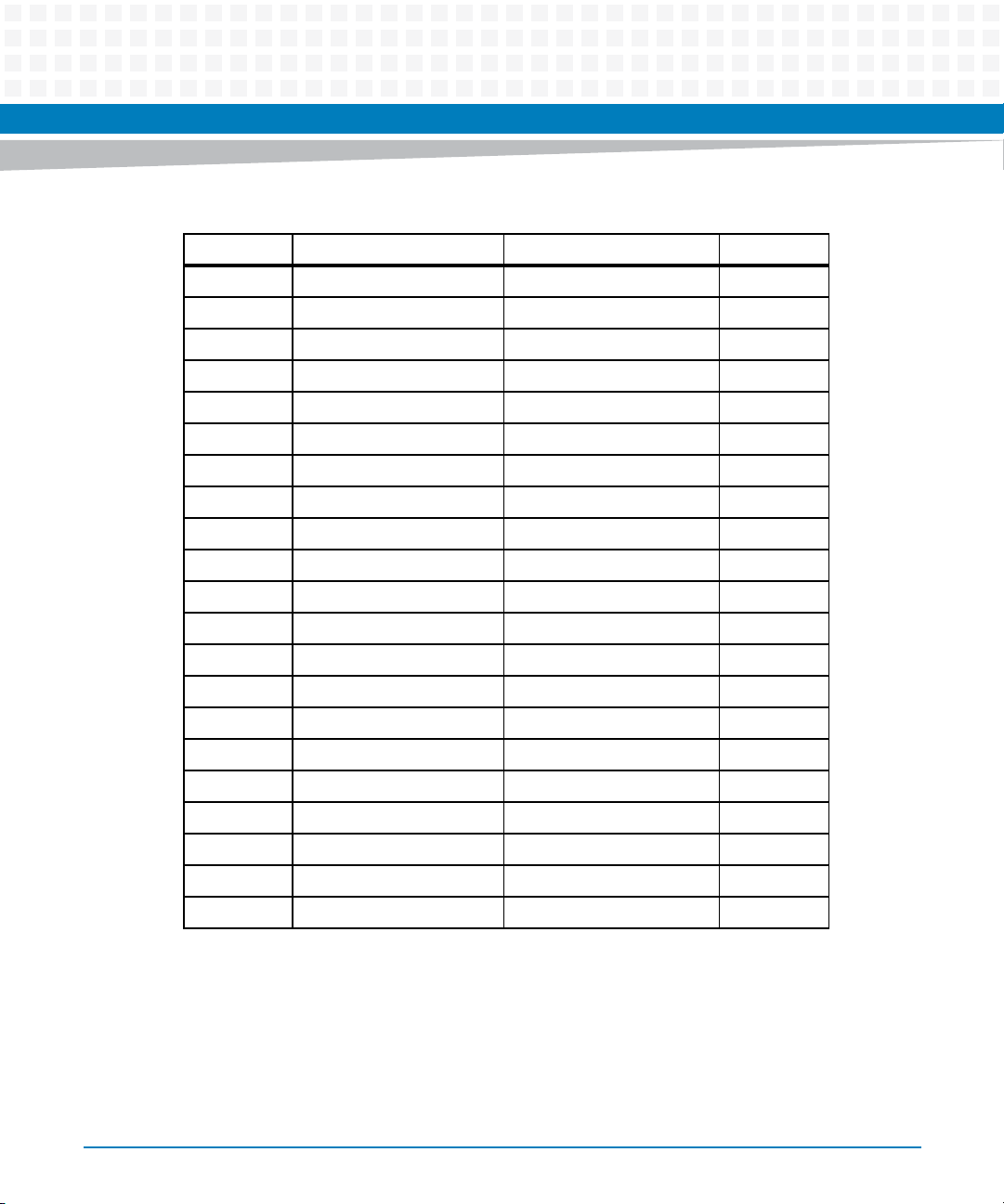
Connector Pin Assignments
Table 4-11 VME Connector (3-Row P2 adapter) (continued)
Pin Signal Signal Pin
12 PRD1 TXD4 44
13 PRD4 GND 45
14 PRD3 RXD4 46
15 PRD6 GND 47
16 PRD5 RTS4 48
17 GND GND 49
18 PRD7 TRXC4 50
19 GND DTR4 51
20 PRACK_L CTS4 52
21 PRPE GND 53
22 PRBSY DCD4 54
23 PRINIT_L GND 55
24 PRSEL RTXC4 56
25 GND GND 57
26 PRFAULT_L TXD2 58
27 GND GND 59
28 TXD3 RXD2 60
29 GND CTS2 61
30 RXD3 RTS2 62
31 CTS3 DCD2 63
32 RTS3 DTR2 64
MVME7616E Transition Module Installation and Use (6806800A43D)
53
Page 54

Connector Pin Assignments
54
MVME7616E Transition Module Installation and Use (6806800A43D)
Page 55

Page 56

Artesyn Embedded Technologies, Artesyn and the Artesyn Embedded Technologies logo are trademarks and service marks of Artesyn Embedded Technologies, Inc.
All other product or service names are the property of their respective owners.
©
2015 Artesyn Embedded Technologies, Inc.
 Loading...