

Page 1
COMX-CAR-210
Installation and Use
P/N: 6806800L14D
August 2014
Page 2

©
Copyright 2014 Artesyn Embedded Technologies, Inc.
All rights reserved.
Trademarks
Artesyn Embedded Technologies, Artesyn and the Artesyn Embedded Technologies logo are trademarks and service marks of
Artesyn Embedded Technologies, Inc.© 2014 Artesyn Embedded Technologies, Inc. All other product or service names are the
property of their respective owners.
Intel® is a trademark or registered trademark of Intel Corporation or its subsidiaries in the United States and other countries.
Java™ and all other Java-based marks are trademarks or registered trademarks of Oracle America, Inc. in the U.S. and other countries.
Microsoft®, Windows® and Windows Me® are registered trademarks of Microsoft Corporation; and Windows XP™ is a trademark of
Microsoft Corporation.
PICMG®, CompactPCI®, AdvancedTCA™ and the PICMG, CompactPCI and AdvancedTCA logos are registered trademarks of the PCI
Industrial Computer Manufacturers Group.
UNIX® is a registered trademark of The Open Group in the United States and other countries.
Notice
While reasonable efforts have been made to assure the accuracy of this document, Artesyn assumes no liability resulting from any
omissions in this document, or from the use of the information obtained therein. Artesyn reserves the right to revise this document
and to make changes from time to time in the content hereof without obligation of Artesyn to notify any person of such revision or
changes.
Electronic versions of this material may be read online, downloaded for personal use, or referenced in another document as a URL to
an Artesyn website. The text itself may not be published commercially in print or electronic form, edited, translated, or otherwise
altered without the permission of Artesyn.
It is possible that this publication may contain reference to or information about Artesyn products (machines and programs),
programming, or services that are not available in your country. Such references or information must not be construed to mean that
Artesyn intends to announce such Artesyn products, programming, or services in your country.
Limited and Restricted Rights Legend
If the documentation contained herein is supplied, directly or indirectly, to the U.S. Government, the following notice shall apply
unless otherwise agreed to in writing by Artesyn.
Use, duplication, or disclosure by the Government is subject to restrictions as set forth in subparagraph (b)(3) of the Rights in
Technical Data clause at DFARS 252.227-7013 (Nov. 1995) and of the Rights in Noncommercial Computer Software and
Documentation clause at DFARS 252.227-7014 (Jun. 1995).
Contact Address
Artesyn Embedded Technologies Artesyn Embedded Technologies
Marketing Communications
2900 S. Diablo Way, Suite 190
Tempe, Arizona 85282
Lilienthalstr. 17-19
85579 Neubiberg/Munich
Germany
Page 3

Contents
Contents
About this Manual . . . . . . . . . . . . . . . . . . . . . . . . . . . . . . . . . . . . . . . . . . . . . . . . . . . . . . . . . . . . . . . . . . . . . . . 11
1 Introduction . . . . . . . . . . . . . . . . . . . . . . . . . . . . . . . . . . . . . . . . . . . . . . . . . . . . . . . . . . . . . . . . . . . . . . . . . 15
1.1 Features . . . . . . . . . . . . . . . . . . . . . . . . . . . . . . . . . . . . . . . . . . . . . . . . . . . . . . . . . . . . . . . . . . . . . . . . . . . 15
1.2 Standard Compliances . . . . . . . . . . . . . . . . . . . . . . . . . . . . . . . . . . . . . . . . . . . . . . . . . . . . . . . . . . . . . . 17
1.3 Mechanical Data . . . . . . . . . . . . . . . . . . . . . . . . . . . . . . . . . . . . . . . . . . . . . . . . . . . . . . . . . . . . . . . . . . . 18
1.4 Ordering Information . . . . . . . . . . . . . . . . . . . . . . . . . . . . . . . . . . . . . . . . . . . . . . . . . . . . . . . . . . . . . . . 19
1.5 Product Information . . . . . . . . . . . . . . . . . . . . . . . . . . . . . . . . . . . . . . . . . . . . . . . . . . . . . . . . . . . . . . . . 20
2 Hardware Preparation and Installation . . . . . . . . . . . . . . . . . . . . . . . . . . . . . . . . . . . . . . . . . . . . . . . . . 21
2.1 Environmental and Power Requirements . . . . . . . . . . . . . . . . . . . . . . . . . . . . . . . . . . . . . . . . . . . . . . 21
2.1.1 Environmental Requirements. . . . . . . . . . . . . . . . . . . . . . . . . . . . . . . . . . . . . . . . . . . . . . . . . . 21
2.1.2 Power Requirements . . . . . . . . . . . . . . . . . . . . . . . . . . . . . . . . . . . . . . . . . . . . . . . . . . . . . . . . . 22
2.2 Unpacking and Inspecting the Board . . . . . . . . . . . . . . . . . . . . . . . . . . . . . . . . . . . . . . . . . . . . . . . . . . 22
2.3 Installation and Removal of the COM Express Module . . . . . . . . . . . . . . . . . . . . . . . . . . . . . . . . . . . 23
2.4 Replacing the Onboard Battery . . . . . . . . . . . . . . . . . . . . . . . . . . . . . . . . . . . . . . . . . . . . . . . . . . . . . . . 24
3 Controls, LEDs, and Connectors . . . . . . . . . . . . . . . . . . . . . . . . . . . . . . . . . . . . . . . . . . . . . . . . . . . . . . . . 25
3.1 Carrier Board Layout . . . . . . . . . . . . . . . . . . . . . . . . . . . . . . . . . . . . . . . . . . . . . . . . . . . . . . . . . . . . . . . . 25
3.2 COM Express Board-to-Board Connector . . . . . . . . . . . . . . . . . . . . . . . . . . . . . . . . . . . . . . . . . . . . . . 26
3.3 LEDs . . . . . . . . . . . . . . . . . . . . . . . . . . . . . . . . . . . . . . . . . . . . . . . . . . . . . . . . . . . . . . . . . . . . . . . . . . . . . . 30
3.4 Connectors . . . . . . . . . . . . . . . . . . . . . . . . . . . . . . . . . . . . . . . . . . . . . . . . . . . . . . . . . . . . . . . . . . . . . . . . 30
3.4.1 Video . . . . . . . . . . . . . . . . . . . . . . . . . . . . . . . . . . . . . . . . . . . . . . . . . . . . . . . . . . . . . . . . . . . . . . . 31
3.4.1.1 LVDS . . . . . . . . . . . . . . . . . . . . . . . . . . . . . . . . . . . . . . . . . . . . . . . . . . . . . . . . . . . . . . 31
3.4.1.2 VGA . . . . . . . . . . . . . . . . . . . . . . . . . . . . . . . . . . . . . . . . . . . . . . . . . . . . . . . . . . . . . . . 33
3.4.1.3 SDVO to DVI . . . . . . . . . . . . . . . . . . . . . . . . . . . . . . . . . . . . . . . . . . . . . . . . . . . . . . . 33
3.4.2 Audio. . . . . . . . . . . . . . . . . . . . . . . . . . . . . . . . . . . . . . . . . . . . . . . . . . . . . . . . . . . . . . . . . . . . . . . 34
3.4.2.1 Audio Jack . . . . . . . . . . . . . . . . . . . . . . . . . . . . . . . . . . . . . . . . . . . . . . . . . . . . . . . . . 34
3.4.2.2 Audio Header . . . . . . . . . . . . . . . . . . . . . . . . . . . . . . . . . . . . . . . . . . . . . . . . . . . . . . 35
3.4.3 LAN . . . . . . . . . . . . . . . . . . . . . . . . . . . . . . . . . . . . . . . . . . . . . . . . . . . . . . . . . . . . . . . . . . . . . . . . 36
3.4.4 PCI Express . . . . . . . . . . . . . . . . . . . . . . . . . . . . . . . . . . . . . . . . . . . . . . . . . . . . . . . . . . . . . . . . . . 36
3.4.5 USB . . . . . . . . . . . . . . . . . . . . . . . . . . . . . . . . . . . . . . . . . . . . . . . . . . . . . . . . . . . . . . . . . . . . . . . . 37
3.4.5.1 USB 2.0 . . . . . . . . . . . . . . . . . . . . . . . . . . . . . . . . . . . . . . . . . . . . . . . . . . . . . . . . . . . . 37
3.4.6 Storage . . . . . . . . . . . . . . . . . . . . . . . . . . . . . . . . . . . . . . . . . . . . . . . . . . . . . . . . . . . . . . . . . . . . . 38
COMX-CAR-210 Installation and Use (6806800L14D)
3
Page 4

Contents
Contents
Contents
3.4.6.1 SATA . . . . . . . . . . . . . . . . . . . . . . . . . . . . . . . . . . . . . . . . . . . . . . . . . . . . . . . . . . . . . . 38
3.4.6.2 IDE . . . . . . . . . . . . . . . . . . . . . . . . . . . . . . . . . . . . . . . . . . . . . . . . . . . . . . . . . . . . . . . . 39
3.4.6.3 CF Card . . . . . . . . . . . . . . . . . . . . . . . . . . . . . . . . . . . . . . . . . . . . . . . . . . . . . . . . . . . . 40
3.4.7 Super I/O. . . . . . . . . . . . . . . . . . . . . . . . . . . . . . . . . . . . . . . . . . . . . . . . . . . . . . . . . . . . . . . . . . . . 42
3.4.7.1 Fan . . . . . . . . . . . . . . . . . . . . . . . . . . . . . . . . . . . . . . . . . . . . . . . . . . . . . . . . . . . . . . . . 42
3.4.7.2 PS/2 . . . . . . . . . . . . . . . . . . . . . . . . . . . . . . . . . . . . . . . . . . . . . . . . . . . . . . . . . . . . . . . 43
3.4.7.3 LPT Port . . . . . . . . . . . . . . . . . . . . . . . . . . . . . . . . . . . . . . . . . . . . . . . . . . . . . . . . . . . 43
3.4.7.4 Serial Ports . . . . . . . . . . . . . . . . . . . . . . . . . . . . . . . . . . . . . . . . . . . . . . . . . . . . . . . . 44
3.5 Headers . . . . . . . . . . . . . . . . . . . . . . . . . . . . . . . . . . . . . . . . . . . . . . . . . . . . . . . . . . . . . . . . . . . . . . . . . . . 46
3.5.1 Low Pin Count . . . . . . . . . . . . . . . . . . . . . . . . . . . . . . . . . . . . . . . . . . . . . . . . . . . . . . . . . . . . . . . 46
3.5.2 Trusted Platform Module. . . . . . . . . . . . . . . . . . . . . . . . . . . . . . . . . . . . . . . . . . . . . . . . . . . . . . 47
3.5.3 GPIO . . . . . . . . . . . . . . . . . . . . . . . . . . . . . . . . . . . . . . . . . . . . . . . . . . . . . . . . . . . . . . . . . . . . . . . 47
3.5.4 SMBus . . . . . . . . . . . . . . . . . . . . . . . . . . . . . . . . . . . . . . . . . . . . . . . . . . . . . . . . . . . . . . . . . . . . . . 48
3.5.5 Miscellaneous I/O . . . . . . . . . . . . . . . . . . . . . . . . . . . . . . . . . . . . . . . . . . . . . . . . . . . . . . . . . . . . 49
3.5.6 SPI Flash . . . . . . . . . . . . . . . . . . . . . . . . . . . . . . . . . . . . . . . . . . . . . . . . . . . . . . . . . . . . . . . . . . . . 50
3.5.7 EEPPROM . . . . . . . . . . . . . . . . . . . . . . . . . . . . . . . . . . . . . . . . . . . . . . . . . . . . . . . . . . . . . . . . . . . 51
3.5.8 Jumper Setting Description. . . . . . . . . . . . . . . . . . . . . . . . . . . . . . . . . . . . . . . . . . . . . . . . . . . . 51
4 Functional Description . . . . . . . . . . . . . . . . . . . . . . . . . . . . . . . . . . . . . . . . . . . . . . . . . . . . . . . . . . . . . . . . 55
4.1 Block Diagram . . . . . . . . . . . . . . . . . . . . . . . . . . . . . . . . . . . . . . . . . . . . . . . . . . . . . . . . . . . . . . . . . . . . . 55
4.2 Video . . . . . . . . . . . . . . . . . . . . . . . . . . . . . . . . . . . . . . . . . . . . . . . . . . . . . . . . . . . . . . . . . . . . . . . . . . . . . 55
4.2.1 LVDS . . . . . . . . . . . . . . . . . . . . . . . . . . . . . . . . . . . . . . . . . . . . . . . . . . . . . . . . . . . . . . . . . . . . . . . 55
4.2.2 VGA . . . . . . . . . . . . . . . . . . . . . . . . . . . . . . . . . . . . . . . . . . . . . . . . . . . . . . . . . . . . . . . . . . . . . . . . 56
4.2.3 SDVO to DVI. . . . . . . . . . . . . . . . . . . . . . . . . . . . . . . . . . . . . . . . . . . . . . . . . . . . . . . . . . . . . . . . . 56
4.3 Audio . . . . . . . . . . . . . . . . . . . . . . . . . . . . . . . . . . . . . . . . . . . . . . . . . . . . . . . . . . . . . . . . . . . . . . . . . . . . . 56
4.3.1 Audio Jack. . . . . . . . . . . . . . . . . . . . . . . . . . . . . . . . . . . . . . . . . . . . . . . . . . . . . . . . . . . . . . . . . . . 56
4.3.2 Audio Header. . . . . . . . . . . . . . . . . . . . . . . . . . . . . . . . . . . . . . . . . . . . . . . . . . . . . . . . . . . . . . . . 56
4.4 LAN . . . . . . . . . . . . . . . . . . . . . . . . . . . . . . . . . . . . . . . . . . . . . . . . . . . . . . . . . . . . . . . . . . . . . . . . . . . . . . . 57
4.5 PCI . . . . . . . . . . . . . . . . . . . . . . . . . . . . . . . . . . . . . . . . . . . . . . . . . . . . . . . . . . . . . . . . . . . . . . . . . . . . . . . 57
4.6 PCI Express . . . . . . . . . . . . . . . . . . . . . . . . . . . . . . . . . . . . . . . . . . . . . . . . . . . . . . . . . . . . . . . . . . . . . . . . 58
4.6.1 PCIe Mini-Card for WiFi/WiMAX . . . . . . . . . . . . . . . . . . . . . . . . . . . . . . . . . . . . . . . . . . . . . . . . 59
4.7 USB . . . . . . . . . . . . . . . . . . . . . . . . . . . . . . . . . . . . . . . . . . . . . . . . . . . . . . . . . . . . . . . . . . . . . . . . . . . . . . . 59
4.8 Storage . . . . . . . . . . . . . . . . . . . . . . . . . . . . . . . . . . . . . . . . . . . . . . . . . . . . . . . . . . . . . . . . . . . . . . . . . . . 59
4.8.1 SATA . . . . . . . . . . . . . . . . . . . . . . . . . . . . . . . . . . . . . . . . . . . . . . . . . . . . . . . . . . . . . . . . . . . . . . . 60
4.8.2 IDE . . . . . . . . . . . . . . . . . . . . . . . . . . . . . . . . . . . . . . . . . . . . . . . . . . . . . . . . . . . . . . . . . . . . . . . . . 60
4
COMX-CAR-210 Installation and Use (6806800L14D)
Page 5

Contents
4.8.3 CF Card . . . . . . . . . . . . . . . . . . . . . . . . . . . . . . . . . . . . . . . . . . . . . . . . . . . . . . . . . . . . . . . . . . . . . 60
4.9 Super I/O . . . . . . . . . . . . . . . . . . . . . . . . . . . . . . . . . . . . . . . . . . . . . . . . . . . . . . . . . . . . . . . . . . . . . . . . . . 60
4.9.1 Voltage and Thermal Monitoring. . . . . . . . . . . . . . . . . . . . . . . . . . . . . . . . . . . . . . . . . . . . . . . 61
4.9.2 Fan Control. . . . . . . . . . . . . . . . . . . . . . . . . . . . . . . . . . . . . . . . . . . . . . . . . . . . . . . . . . . . . . . . . . 61
4.9.3 PS/2 . . . . . . . . . . . . . . . . . . . . . . . . . . . . . . . . . . . . . . . . . . . . . . . . . . . . . . . . . . . . . . . . . . . . . . . . 61
4.9.4 LPT . . . . . . . . . . . . . . . . . . . . . . . . . . . . . . . . . . . . . . . . . . . . . . . . . . . . . . . . . . . . . . . . . . . . . . . . . 62
4.9.5 RS-232 and RS-422/485 Ports . . . . . . . . . . . . . . . . . . . . . . . . . . . . . . . . . . . . . . . . . . . . . . . . . 62
4.10 SPI Flash . . . . . . . . . . . . . . . . . . . . . . . . . . . . . . . . . . . . . . . . . . . . . . . . . . . . . . . . . . . . . . . . . . . . . . . . . . . 63
4.11 Watchdog Timer . . . . . . . . . . . . . . . . . . . . . . . . . . . . . . . . . . . . . . . . . . . . . . . . . . . . . . . . . . . . . . . . . . . 64
4.12 Real Time Clock (RTC) . . . . . . . . . . . . . . . . . . . . . . . . . . . . . . . . . . . . . . . . . . . . . . . . . . . . . . . . . . . . . . . 64
A Related Documentation . . . . . . . . . . . . . . . . . . . . . . . . . . . . . . . . . . . . . . . . . . . . . . . . . . . . . . . . . . . . . . . 65
A.1 Artesyn Embedded Technologies - Embedded Computing Documentation . . . . . . . . . . . . . . . . 65
Safety Notes . . . . . . . . . . . . . . . . . . . . . . . . . . . . . . . . . . . . . . . . . . . . . . . . . . . . . . . . . . . . . . . . . . . . . . . . . . . . . 67
Sicherheitshinweise . . . . . . . . . . . . . . . . . . . . . . . . . . . . . . . . . . . . . . . . . . . . . . . . . . . . . . . . . . . . . . . . . . . . . . 71
COMX-CAR-210 Installation and Use (6806800L14D)
5
Page 6

Contents
Contents
Contents
6
COMX-CAR-210 Installation and Use (6806800L14D)
Page 7

List of Tables
Table 1-1 Carrier Board Features . . . . . . . . . . . . . . . . . . . . . . . . . . . . . . . . . . . . . . . . . . . . . . . . . . . . . . . . . . 15
Table 1-2 Board Variants . . . . . . . . . . . . . . . . . . . . . . . . . . . . . . . . . . . . . . . . . . . . . . . . . . . . . . . . . . . . . . . . . 19
Table 2-1 Environmental Requirements . . . . . . . . . . . . . . . . . . . . . . . . . . . . . . . . . . . . . . . . . . . . . . . . . . . . 21
Table 2-2 Power requirement . . . . . . . . . . . . . . . . . . . . . . . . . . . . . . . . . . . . . . . . . . . . . . . . . . . . . . . . . . . . 22
Table 3-1 COM EXPRESS Connector Pin Definition . . . . . . . . . . . . . . . . . . . . . . . . . . . . . . . . . . . . . . . . . . 26
Table 3-2 LED function description . . . . . . . . . . . . . . . . . . . . . . . . . . . . . . . . . . . . . . . . . . . . . . . . . . . . . . . . 30
Table 3-3 P8, LVDS Inverter Header Pin-out . . . . . . . . . . . . . . . . . . . . . . . . . . . . . . . . . . . . . . . . . . . . . . . . . 31
Table 3-4 P6, LVDS Connector Pin Definition . . . . . . . . . . . . . . . . . . . . . . . . . . . . . . . . . . . . . . . . . . . . . . . 31
Table 3-5 P7, LVDS Power Supply Jumper Configuration . . . . . . . . . . . . . . . . . . . . . . . . . . . . . . . . . . . . . . 32
Table 3-6 P35, LVDS Power Supply Jumper Configuration . . . . . . . . . . . . . . . . . . . . . . . . . . . . . . . . . . . . 32
Table 3-7 P26, 5V Stand-by Jumper Setting . . . . . . . . . . . . . . . . . . . . . . . . . . . . . . . . . . . . . . . . . . . . . . . . . 33
Table 3-8 J5, VGA Connector Pin-out . . . . . . . . . . . . . . . . . . . . . . . . . . . . . . . . . . . . . . . . . . . . . . . . . . . . . . 33
Table 3-9 P13, SDVO to DVI Jumper Setting . . . . . . . . . . . . . . . . . . . . . . . . . . . . . . . . . . . . . . . . . . . . . . . . 33
Table 3-10 J5, DVI Connector Pin-out . . . . . . . . . . . . . . . . . . . . . . . . . . . . . . . . . . . . . . . . . . . . . . . . . . . . . . . 34
Table 3-11 J10, Audio Jack Pin-out . . . . . . . . . . . . . . . . . . . . . . . . . . . . . . . . . . . . . . . . . . . . . . . . . . . . . . . . . . 34
Table 3-12 P11, Audio Header 1 Pin-out . . . . . . . . . . . . . . . . . . . . . . . . . . . . . . . . . . . . . . . . . . . . . . . . . . . . . 35
Table 3-13 P53, Audio Header 2 Pin-out . . . . . . . . . . . . . . . . . . . . . . . . . . . . . . . . . . . . . . . . . . . . . . . . . . . . . 35
Table 3-14 P50, P51, P52 Jumper setting for side-surround output . . . . . . . . . . . . . . . . . . . . . . . . . . . . . 35
Table 3-15 J1, LAN Connectors Pin-Out . . . . . . . . . . . . . . . . . . . . . . . . . . . . . . . . . . . . . . . . . . . . . . . . . . . . . 36
Table 3-16 P13, PCIe MUX Configuration . . . . . . . . . . . . . . . . . . . . . . . . . . . . . . . . . . . . . . . . . . . . . . . . . . . . 36
Table 3-17 P25, PCIe MUX Configuration . . . . . . . . . . . . . . . . . . . . . . . . . . . . . . . . . . . . . . . . . . . . . . . . . . . . 36
Table 3-18 J15, Dual USB 2.0 x2 ports on rear IO Pin-out . . . . . . . . . . . . . . . . . . . . . . . . . . . . . . . . . . . . . . 37
Table 3-19 P14, One USB 2.0 Header . . . . . . . . . . . . . . . . . . . . . . . . . . . . . . . . . . . . . . . . . . . . . . . . . . . . . . . 37
Table 3-20 P15, USB 2.0 Header for eUSB Flash . . . . . . . . . . . . . . . . . . . . . . . . . . . . . . . . . . . . . . . . . . . . . . 38
Table 3-21 P10, USB MUX Configuration . . . . . . . . . . . . . . . . . . . . . . . . . . . . . . . . . . . . . . . . . . . . . . . . . . . . 38
Table 3-22 J11-J12, SATA Sockets Pin-out . . . . . . . . . . . . . . . . . . . . . . . . . . . . . . . . . . . . . . . . . . . . . . . . . . . . 38
Table 3-23 P38 & J14, SATA Sockets Pin-out . . . . . . . . . . . . . . . . . . . . . . . . . . . . . . . . . . . . . . . . . . . . . . . . . 39
Table 3-24 J7 & J14 IDE Socket Pin-out . . . . . . . . . . . . . . . . . . . . . . . . . . . . . . . . . . . . . . . . . . . . . . . . . . . . . . 39
Table 3-25 P39, IDE Master/Slave Jumper Setting . . . . . . . . . . . . . . . . . . . . . . . . . . . . . . . . . . . . . . . . . . . . . 40
Table 3-26 J7 & J14, CF Card Socket Pin-out . . . . . . . . . . . . . . . . . . . . . . . . . . . . . . . . . . . . . . . . . . . . . . . . . . 40
Table 3-27 P9, CF Card Master/Slave Jumper Settings . . . . . . . . . . . . . . . . . . . . . . . . . . . . . . . . . . . . . . . . . 41
Table 3-28 P3, P42, P27, System and Module Fan Headers Pin-out . . . . . . . . . . . . . . . . . . . . . . . . . . . . . 42
Table 3-29 J13, PS/2 Connector Pin-Out . . . . . . . . . . . . . . . . . . . . . . . . . . . . . . . . . . . . . . . . . . . . . . . . . . . . 43
Table 3-30 P32 LPT Header Pin-out . . . . . . . . . . . . . . . . . . . . . . . . . . . . . . . . . . . . . . . . . . . . . . . . . . . . . . . . . 43
Table 3-31 P5, Dual Rear IO RS232 Ports Pin-out . . . . . . . . . . . . . . . . . . . . . . . . . . . . . . . . . . . . . . . . . . . . . 44
Table 3-32 P20, P21, P22, P23 RS232 Headers Pin-Out . . . . . . . . . . . . . . . . . . . . . . . . . . . . . . . . . . . . . . . . 44
COMX-CAR-210 Installation and Use (6806800L14D)
7
Page 8

List of Tables
Table 3-34 P34, P41, PS232, RS422/485 Ports Configuration . . . . . . . . . . . . . . . . . . . . . . . . . . . . . . . . . .45
Table 3-33 P37, P33, RS422/485 Headers Pin-Out . . . . . . . . . . . . . . . . . . . . . . . . . . . . . . . . . . . . . . . . . . . . 45
Table 3-35 P29, Low Pin Count Header Pin-out . . . . . . . . . . . . . . . . . . . . . . . . . . . . . . . . . . . . . . . . . . . . . . .46
Table 3-36 P28 Trust Platform Module Header Pin-out . . . . . . . . . . . . . . . . . . . . . . . . . . . . . . . . . . . . . . . . 47
Table 3-37 P30 Module GPIO Header Pin-Out . . . . . . . . . . . . . . . . . . . . . . . . . . . . . . . . . . . . . . . . . . . . . . . .47
Table 3-38 P19, SIO GPIO Header Pin-Out . . . . . . . . . . . . . . . . . . . . . . . . . . . . . . . . . . . . . . . . . . . . . . . . . . . 48
Table 3-39 P18, SMBus Header Pin-out . . . . . . . . . . . . . . . . . . . . . . . . . . . . . . . . . . . . . . . . . . . . . . . . . . . . . . 48
Table 3-40 P16, Miscellaneous I/O Header Pin-out . . . . . . . . . . . . . . . . . . . . . . . . . . . . . . . . . . . . . . . . . . . . 49
Table 3-41 P47, SF100 Header Pin-out . . . . . . . . . . . . . . . . . . . . . . . . . . . . . . . . . . . . . . . . . . . . . . . . . . . . . . 50
Table 3-42 P46, SPI Flash Configuration . . . . . . . . . . . . . . . . . . . . . . . . . . . . . . . . . . . . . . . . . . . . . . . . . . . . . 50
Table 3-43 P12, BIOS Configuration on the module . . . . . . . . . . . . . . . . . . . . . . . . . . . . . . . . . . . . . . . . . . . 50
Table 3-44 P43, BIOS Configuration on the module . . . . . . . . . . . . . . . . . . . . . . . . . . . . . . . . . . . . . . . . . . . 50
Table 3-45 P45, EEPROM Header Pin-out . . . . . . . . . . . . . . . . . . . . . . . . . . . . . . . . . . . . . . . . . . . . . . . . . . . . 51
Table 3-46 P36 PEG Enable . . . . . . . . . . . . . . . . . . . . . . . . . . . . . . . . . . . . . . . . . . . . . . . . . . . . . . . . . . . . . . . . 51
Table 3-47 P7 LVDS PWR1 Set . . . . . . . . . . . . . . . . . . . . . . . . . . . . . . . . . . . . . . . . . . . . . . . . . . . . . . . . . . . . . . 51
Table 3-48 P25 PCIE Switch . . . . . . . . . . . . . . . . . . . . . . . . . . . . . . . . . . . . . . . . . . . . . . . . . . . . . . . . . . . . . . . . 51
Table 3-49 P17 Case Open . . . . . . . . . . . . . . . . . . . . . . . . . . . . . . . . . . . . . . . . . . . . . . . . . . . . . . . . . . . . . . . . . 52
Table 3-50 P43 SPI1 Boot Sel . . . . . . . . . . . . . . . . . . . . . . . . . . . . . . . . . . . . . . . . . . . . . . . . . . . . . . . . . . . . . . . 52
Table 3-51 P41 COM6 Mode Sel . . . . . . . . . . . . . . . . . . . . . . . . . . . . . . . . . . . . . . . . . . . . . . . . . . . . . . . . . . . . 52
Table 3-52 P39 IDE Master/Slave Set . . . . . . . . . . . . . . . . . . . . . . . . . . . . . . . . . . . . . . . . . . . . . . . . . . . . . . . .52
Table 3-53 P35 LVDS PWR2 Set . . . . . . . . . . . . . . . . . . . . . . . . . . . . . . . . . . . . . . . . . . . . . . . . . . . . . . . . . . . . 52
Table 3-54 P13 SDVO Switch . . . . . . . . . . . . . . . . . . . . . . . . . . . . . . . . . . . . . . . . . . . . . . . . . . . . . . . . . . . . . . . 53
Table 3-55 P46 SF100 PROG PART SEL . . . . . . . . . . . . . . . . . . . . . . . . . . . . . . . . . . . . . . . . . . . . . . . . . . . . . . 53
Table 3-56 P40 PS ON SEL . . . . . . . . . . . . . . . . . . . . . . . . . . . . . . . . . . . . . . . . . . . . . . . . . . . . . . . . . . . . . . . . . 53
Table 3-57 P34 COMS Mode Sel . . . . . . . . . . . . . . . . . . . . . . . . . . . . . . . . . . . . . . . . . . . . . . . . . . . . . . . . . . . .53
Table 3-58 P9 CF Card Master/Slave . . . . . . . . . . . . . . . . . . . . . . . . . . . . . . . . . . . . . . . . . . . . . . . . . . . . . . . . 53
Table 3-59 P10 USB Switch . . . . . . . . . . . . . . . . . . . . . . . . . . . . . . . . . . . . . . . . . . . . . . . . . . . . . . . . . . . . . . . . 54
Table 3-60 P50, P51, P52 Stereo Speaker . . . . . . . . . . . . . . . . . . . . . . . . . . . . . . . . . . . . . . . . . . . . . . . . . . . . 54
Table 3-61 P12 SPI0 Boot Select . . . . . . . . . . . . . . . . . . . . . . . . . . . . . . . . . . . . . . . . . . . . . . . . . . . . . . . . . . . . 54
Table 3-62 P26 Module STB PWR SEL . . . . . . . . . . . . . . . . . . . . . . . . . . . . . . . . . . . . . . . . . . . . . . . . . . . . . . . 54
Table 4-1 PCI Resource Table . . . . . . . . . . . . . . . . . . . . . . . . . . . . . . . . . . . . . . . . . . . . . . . . . . . . . . . . . . . . . 57
Table A-1 Artesyn Embedded Technologies - Embedded Computing Publications . . . . . . . . . . . . . . . 65
8
COMX-CAR-210 Installation and Use (6806800L14D)
Page 9

List of Figures
Figure 1-1 Declaration of Conformity . . . . . . . . . . . . . . . . . . . . . . . . . . . . . . . . . . . . . . . . . . . . . . . . 17
Figure 1-2 COMX-CAR-210 Mechanical Data (Top and side view) . . . . . . . . . . . . . . . . . . . . . . . . 18
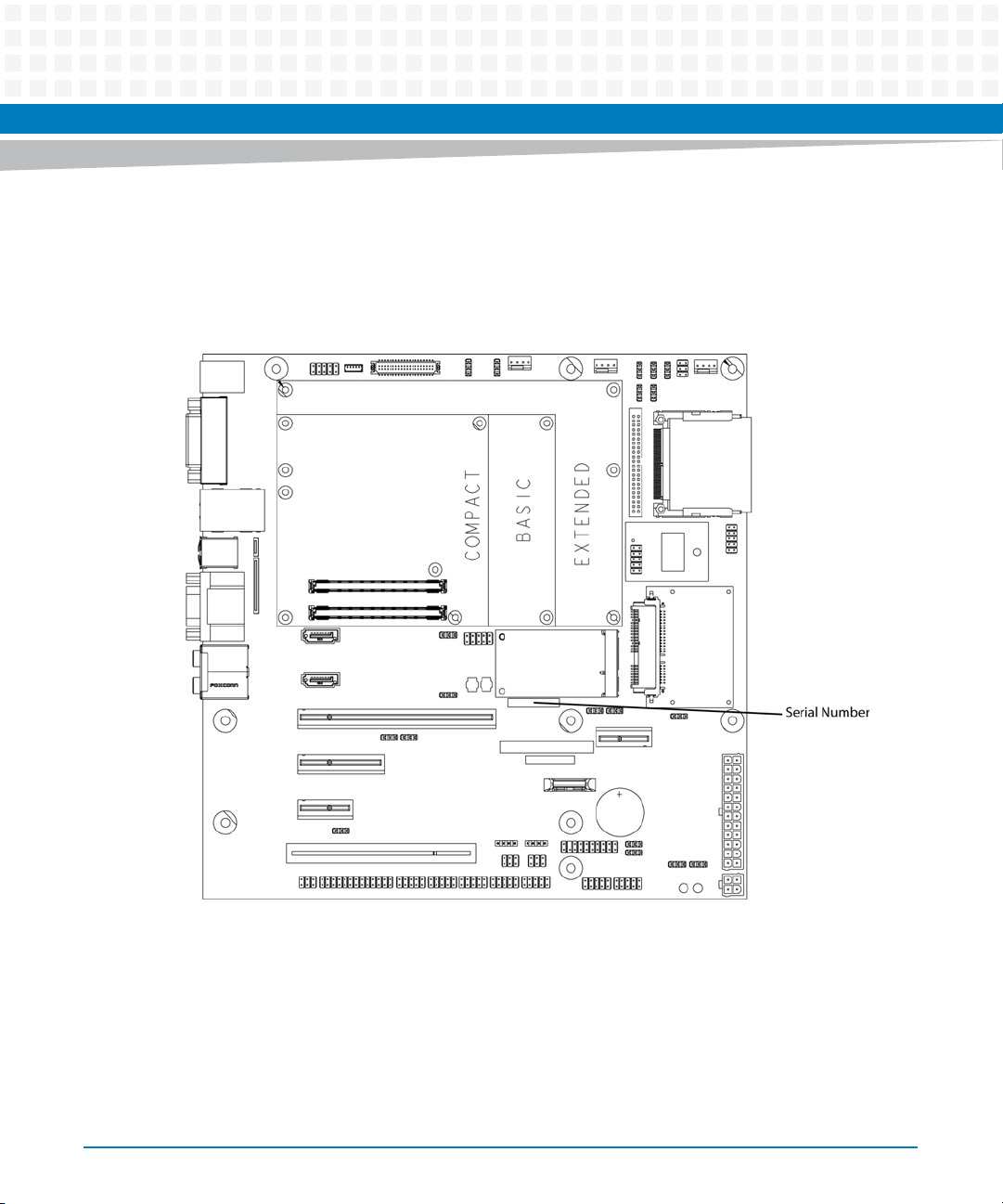
Figure 1-3 COMX-CAR-210 Serial Number . . . . . . . . . . . . . . . . . . . . . . . . . . . . . . . . . . . . . . . . . . . 20
Figure 3-1 COMX-CAR-210 Board Layout . . . . . . . . . . . . . . . . . . . . . . . . . . . . . . . . . . . . . . . . . . . . 25
Figure 3-2 LVDS Inverter Header (P8) . . . . . . . . . . . . . . . . . . . . . . . . . . . . . . . . . . . . . . . . . . . . . . . . 31
Figure 3-3 HDA Audio Header (P11) . . . . . . . . . . . . . . . . . . . . . . . . . . . . . . . . . . . . . . . . . . . . . . . . . 35
Figure 3-4 USB Header (P14, P15) . . . . . . . . . . . . . . . . . . . . . . . . . . . . . . . . . . . . . . . . . . . . . . . . . . . 37
Figure 3-5 FAN Connector (P3, P27, P42) . . . . . . . . . . . . . . . . . . . . . . . . . . . . . . . . . . . . . . . . . . . . 42
Figure 3-6 Serial port header (P20, P21, P22, P23) . . . . . . . . . . . . . . . . . . . . . . . . . . . . . . . . . . . . 45
Figure 3-7 LPC Header (P29) . . . . . . . . . . . . . . . . . . . . . . . . . . . . . . . . . . . . . . . . . . . . . . . . . . . . . . . 46
Figure 3-8 Front Panel Header (P16) . . . . . . . . . . . . . . . . . . . . . . . . . . . . . . . . . . . . . . . . . . . . . . . . . 49
Figure 4-1 Carrier Board Block Diagram . . . . . . . . . . . . . . . . . . . . . . . . . . . . . . . . . . . . . . . . . . . . . . 55
Figure 4-2 Side surround output switch . . . . . . . . . . . . . . . . . . . . . . . . . . . . . . . . . . . . . . . . . . . . . . 57
Figure 4-3 PCI Express block diagram . . . . . . . . . . . . . . . . . . . . . . . . . . . . . . . . . . . . . . . . . . . . . . . . 58
Figure 4-4 PCIe Mini-Card Setting . . . . . . . . . . . . . . . . . . . . . . . . . . . . . . . . . . . . . . . . . . . . . . . . . . . 59
Figure 4-5 Super I/O Block Diagram . . . . . . . . . . . . . . . . . . . . . . . . . . . . . . . . . . . . . . . . . . . . . . . . . 61
Figure 4-6 SPI Flash Block Diagram . . . . . . . . . . . . . . . . . . . . . . . . . . . . . . . . . . . . . . . . . . . . . . . . . . 63
Figure 4-7 Watchdog Timer Block Diagram . . . . . . . . . . . . . . . . . . . . . . . . . . . . . . . . . . . . . . . . . . 64
COMX-CAR-210 Installation and Use (6806800L14D)
9
Page 10

List of Figures
10
COMX-CAR-210 Installation and Use (6806800L14D)
Page 11
About this Manual
Overview of Contents
This manual is divided into the following chapters and appendices.
Introduction provides an overview of the product's features.
Hardware Preparation and Installation provides instructions on installing and removing the
module.
Controls, LEDs, and Connectors provides information on the pin assignments of the various
connectors on the board.
Functional Description discuss the functions of various components on the board.
Related Documentation lists the related documents.
Safety Notes provides a summary of the safety notices applicable to the product.
Sicherheitshinweise is a German version of the Safety Notes.
Abbreviations
This document uses the following abbreviations:
Abbreviation Definition
ANSI American National Standard Institute
ASIC Application Specific Integrated Circuit
ACPI Advanced Configuration and Power Interface
BIOS Basic Input/Output System
BLT Block Transfer
COM Communications
DVI Digital Visual Interface
EEPROM Electrically Erasable Programmable Read-Only Memory
EPROM Erasable Programmable Read-Only Memory
EHCI Enhanced Host Controller Interface
IEEE Institute of Electrical and Electronic Engineers
I2C Inter IC
COMX-CAR-210 Installation and Use (6806800L14D)
11
Page 12
About this Manual
Abbreviation Definition
LFM Linear Feer per Minute
LVDS Low Voltage Differential Signaling
MII Media Independent Interface
PEG PCI Express Graphics
PCI Peripheral Component Interconnect
PIC Programmable Interrupt Controller
RTC Real-Time Clock
SATA Serial Advanced Technology Attachment
SPI Serial Peripheral Interface
SSD Solid State Disk
SDVO Serialized Digital Video Output
UHCI Universal Host Controller Interface
About this Manual
VGA Visual Graphic Array
Conventions
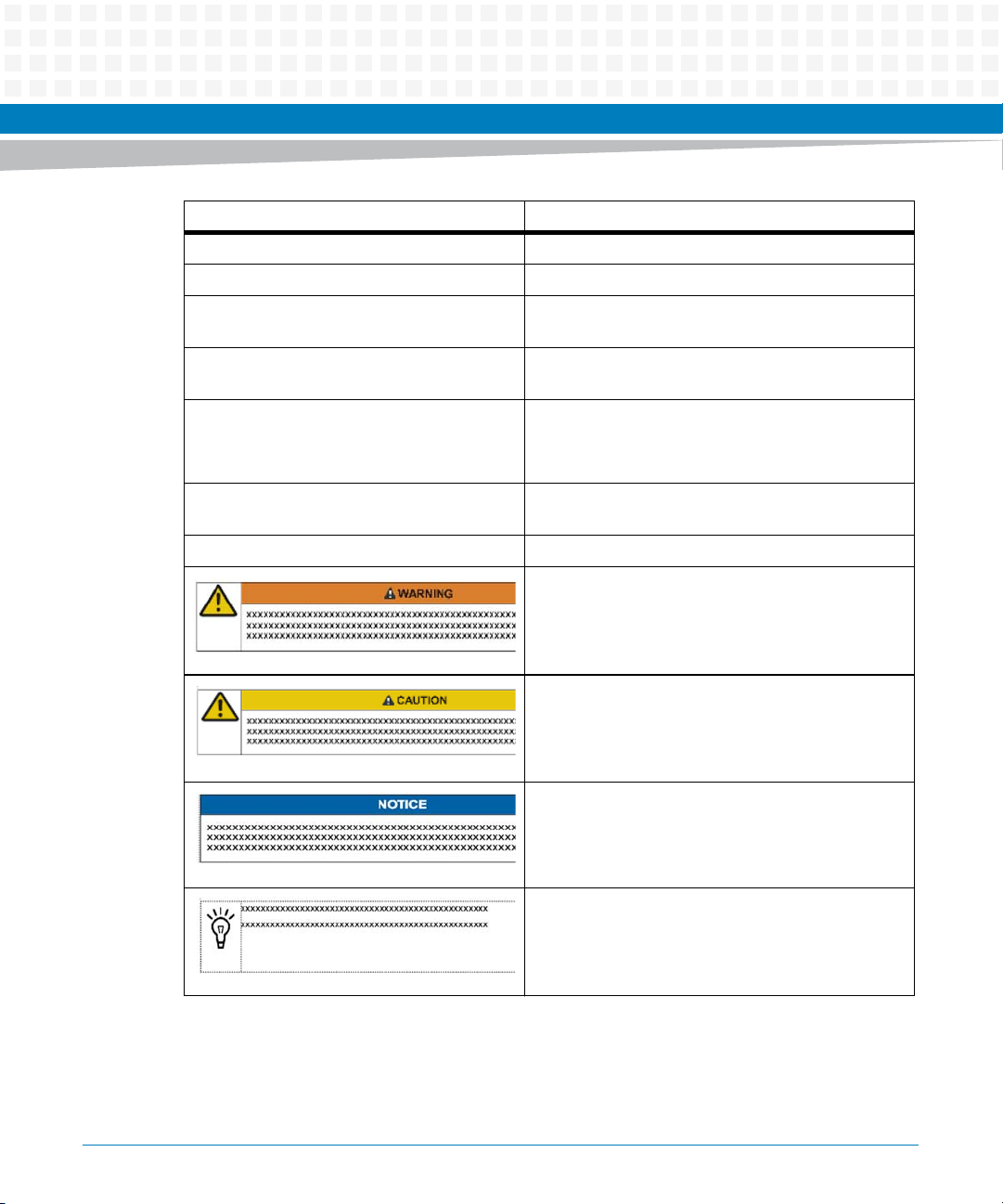
The following table describes the conventions used throughout this manual.
Notation Description
0x00000000 Typical notation for hexadecimal numbers (digits are
0b0000 Same for binary numbers (digits are 0 and 1)
bold Used to emphasize a word
Screen Used for on-screen output and code related elements
Courier + Bold Used to characterize user input and to separate it
Reference Used for references and for table and figure descrip-
12
0 through F), for example used for addresses and offsets
or commands in body text
from system output
tions
COMX-CAR-210 Installation and Use (6806800L14D)
Page 13
About this Manual
Notation Description
File > Exit Notation for selecting a submenu
<text> Notation for variables and keys
[text] Notation for software buttons to click on the screen
and parameter description
... Repeated item for example node 1, node 2, ..., node
12
.
.
.
.. Ranges, for example: 0..4 means one of the integers
| Logical OR
Omission of information from example/command
that is not necessary at the time being
0,1,2,3, and 4 (used in registers)
Indicates a hazardous situation which, if not avoided,
could result in death or serious injury
Indicates a hazardous situation which, if not avoided,
may result in minor or moderate injury
Indicates a property damage message
No danger encountered. Pay attention to important
information
COMX-CAR-210 Installation and Use (6806800L14D)
13
Page 14
About this Manual
Summary of Changes
This manual has been revised and replaces all prior editions.
Part Number Publication Date Description
6806800L14A June 2010 Creation of document, first draft
6806800L14B July 2010 Second draft, updated information, added decla-
6806800L14B August 2010 Third draft, updated figures, updated saftey
6806800L14C December 2012 UpdatedStandard Compliances on page 17
6806800L14D August 2014 Re-branded to Artesyn template.
About this Manual
ration of conformity, mechanical informtion, etc.
notes, edited tables.
Added Declaration of Conformity on page19.
14
COMX-CAR-210 Installation and Use (6806800L14D)
Page 15
Introduction
1.1 Features
The COMX-CAR-210 Express Carrier Board is a Type 2 carrier board. It is designed to support
the COM Express Type 2 specification and is compatible with the COM Express Type 1
specification. This board supports the following COM Express factors: compact, basic and
extended.
Table 1-1 Carrier Board Features
Feature Description
Form factor Micro-ATX (9.6" x 9.6")
Video One LVDS connector
Audio One audio header: MICIN, LOUT, CEN & LEF, Surround, SIDES-
Chapter 1
One DVI & VGA connector
URR, LIN
Two internal headers: MIC IN, Stereo Headphone Out, Stereo
Speaker Out (Multiply used with SIDESURR Out)
LPT One LPT header from Super I/O
KBMS One PS/2 keyboard and mouse connector
COM Four RS232 ports (COM1-COM4)
Two RS232/RS422/RS485 ports
LAN One GbE from COM-E to the RJ45 connector
USB Four USB 2.0 ports on rear IO
One internal header for two USB 2.0 ports
One eUSB flash header (two USB ports implemented, one is mul-
tiplied with Mini-PCIE slot)
PCIe slot One PCIe x16 slot
One PCIe x4 slot
Two PCIe x1 slots (one is optional)
PCI slot One 32-bit PCI slot
CF card One CF card slot, supports both Type I and Type II CF cards
PCIe Mini-card One PCIe Mini-card for WiFi or WiMax
COMX-CAR-210 Installation and Use (6806800L14D)
15
Page 16
Introduction
Table 1-1 Carrier Board Features (continued)
Feature Description
Serial ATA Two seven-pin SATA-II ports
SPI Two SPI sockets with BIOS. Disable headers are implemented.
Trusted Platform Module One onboard TPM header
GPIO Two GPIO headers. One is direct from the module, the other is from
SMbus One SMbus header from module for customer’s use
Power supply One 24-pin ATX power header
One twenty-two pin right-angle SSD connector
One twenty-two pin vertical power SATA connector
One SF100 header to support the onboard program
the SIO WG83624UHG.
One 4-pin ATX 12V header
One header for option to use 5V stand-by module or not
Hardware Monitor and
Controller
Supported module size Compact form-factor
Standard compliance COM Express Module Base Specification revision 2.0
Three-channel voltage sensors: 5V, 3.3V and 12V
Two-channel temperature sensors: module and system
Three-channel fan speed control: one module fan and two sys-
tem fans
Basic form-factor
Extended form-factor
PCI Express Mini Card Electromechanical Specification revision
1.0
PCI Express revision 1.1
PCI Local Bus revision 2.3
SMBus Version 2.0
Universal Host Controller Interface revision 1.1 (UHCI)
Enhanced Host Controller Interface specification for Universal
Serial Bus revision 1.0 (EHCI)
Serial ATA II: extensions to SATA 1.0, revision 1.0
VESA specification
PC 2001 compliance
ACPI
16
COMX-CAR-210 Installation and Use (6806800L14D)
Page 17
1.2 Standard Compliances
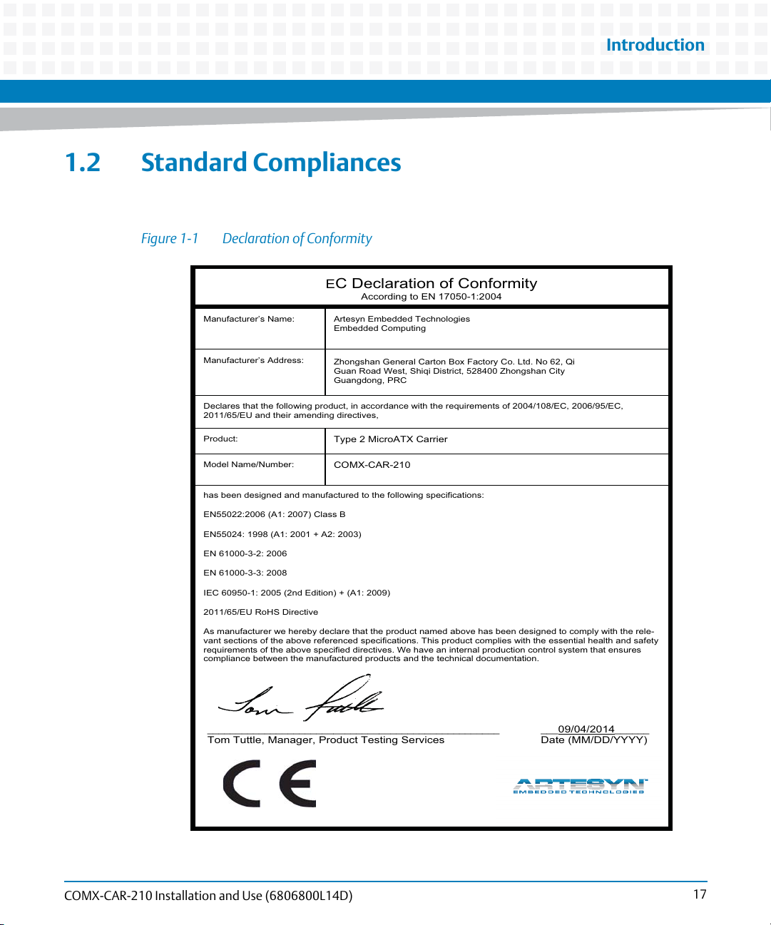
Figure 1-1 Declaration of Conformity
E
C Declaration of Conformity
According to EN 17050-1:2004
Manufacturer’s Name:
Artesyn Embedded Technologies
Embedded Computing
Introduction
Manufacturer’s Address:
Declares that the following product, in accordance with the requirements of 2004/108/EC, 2006/95/EC,
2011/65/EU and their amending directives,
Product:
Model Name/Number:
has been designed and manufactured to the following specifications:
EN55022:2006 (A1: 2007) Class B
EN55024: 1998 (A1: 2001 + A2: 2003)
EN 61000-3-2: 2006
EN 61000-3-3: 2008
IEC 60950-1: 2005 (2nd Edition) + (A1: 2009)
2011/65/EU RoHS Directive
As manufacturer we hereby declare that the product named above has been designed to comply with the rele-
vant sections of the above referenced specifications. This product complies with the essential health and safety
requirements of the above specified directives. We have an internal production control system that ensures
compliance between the manufactured products and the technical documentation.
___________________________________________________ ___
Tom Tuttle, Manager, Product Testing Services Date (MM/DD/YYYY)
Zhongshan General Carton Box Factory Co. Ltd. No 62, Qi
Guan Road West, Shiqi District, 528400 Zhongshan City
Guangdong, PRC
Type 2 MicroATX Carrier
COMX-CAR-210
09/04/2014
______
COMX-CAR-210 Installation and Use (6806800L14D)
17
Page 18
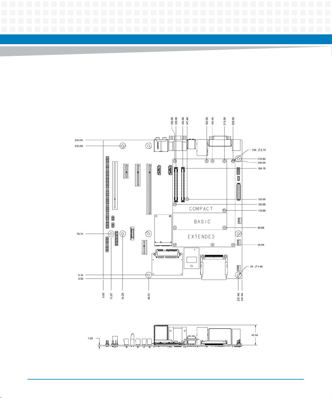
Introduction
1.3 Mechanical Data
Figure 1-2 COMX-CAR-210 Mechanical Data (Top and side view)
18
COMX-CAR-210 Installation and Use (6806800L14D)
Page 19
1.4 Ordering Information
Table 1-2 Board Variants
Order Number Description
TYPE 2 CARRIER MICROATX COMX-CAR-210
Introduction
COMX-CAR-210 Installation and Use (6806800L14D)
19
Page 20
Introduction
1.5 Product Information
This section shows the location of the serial number on the COMX-CAR-210.
Figure 1-3 COMX-CAR-210 Serial Number
20
COMX-CAR-210 Installation and Use (6806800L14D)
Page 21
Hardware Preparation and Installation
2.1 Environmental and Power Requirements
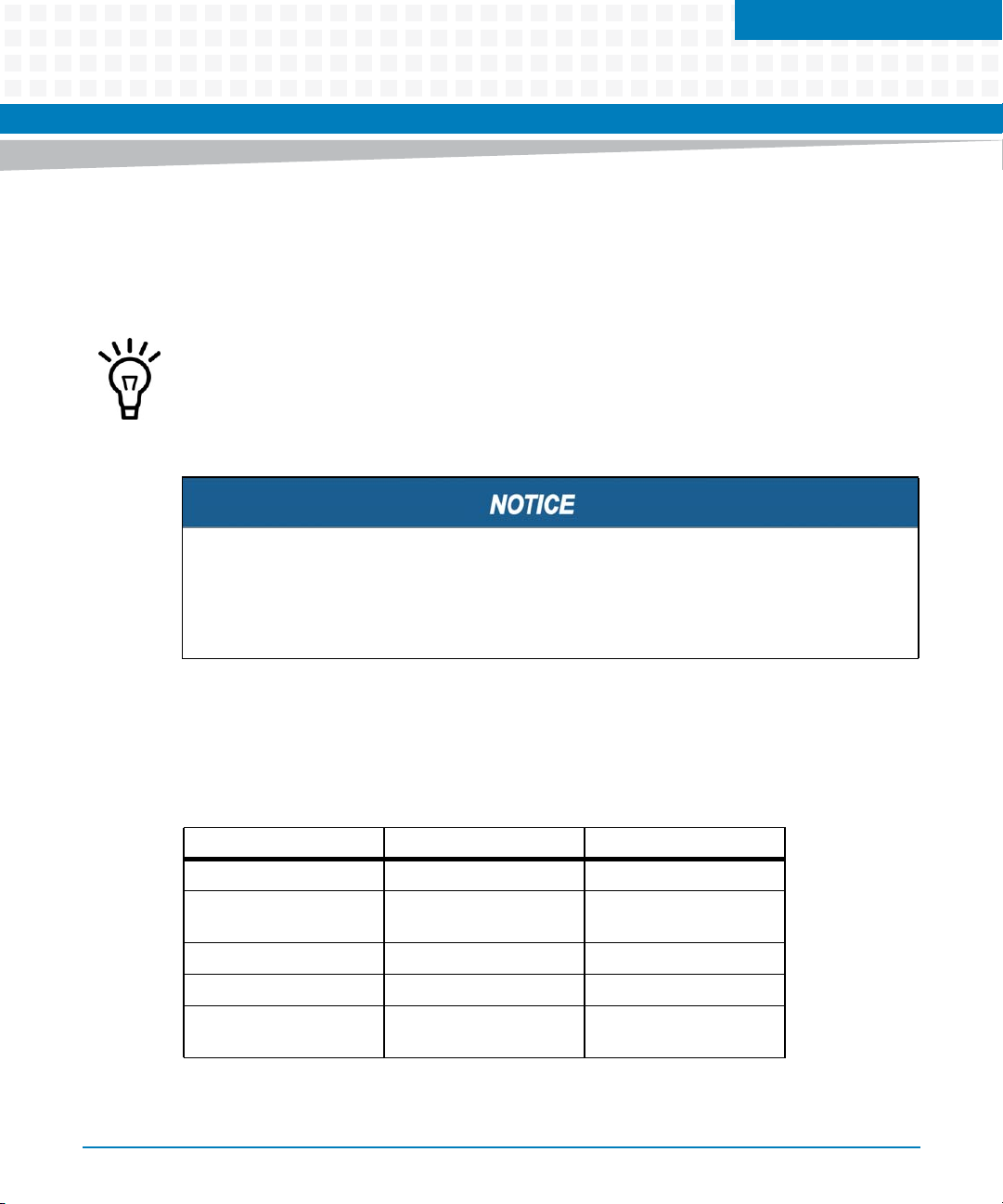
The following table lists the environmentl requirments that the board must meet when
operated in your particular system configuration.
Operating temperatures refer to the temperature of the air circulating around the board and
not to the component temperature.
Product Damage
High humidity and condensation on surfaces causes short circuits.
Do not operate the system outside the specified environmental limits. Make sure the product is completely dry and there is no moisture on any surface before applying power.
Chapter 2
2.1.1 Environmental Requirements
Table 2-1 Environmental Requirements
Environmental Factor Operating Non-Operating
Temperature 0 to +55° C -40 to +85° C
Vibration 0.01g ^2/Hz at 5-500 Hz
Random Vibration
Shock 20g 11 ms sine or saw
Air Flow 400 LFM at 0 to 55°C
Humidity 10-90% (non-condens-
ing)
COMX-CAR-210 Installation and Use (6806800L14D)
21
Page 22
Hardware Preparation and Installation
2.1.2 Power Requirements
The COMX-CAR-210 uses a single 12V power solution where all types of power except the
standby power on the board are generated from the VCC12V. This design consideration is for
the single power input application on most of the industrial usage.
Table 2-2 Power requirement
Voltage 12V 5V_STB
Maximum Current 15A 2A
Maximum Power consumption
190W
2.2 Unpacking and Inspecting the Board
Damage of Circuits
Electrostatic discharge as well as incorrect installation and removal of the product can damage circuits or shorten its life.
Before touching the product, make sure that you are working in an ESD-safe environment;
and wearing ESD wrist strap or ESD shoes. Hold the product by its edges and do not touch
any components or circuits.
1. Verify that you have received all items of your shipment:
Printed Quick Start Guide and Safety Notes
COMX-CAR-210 COM Express Carrier Board
22
Accessories:
– URAT cable, 2x5 pin housing for DB9 pin connector, with I/O panel, 300 mm
length
– USB cable, 2x5 pin housing for USB x2 connector, with I/O panel, 300 mm length
COMX-CAR-210 Installation and Use (6806800L14D)
Page 23
Hardware Preparation and Installation
– LPT cable, 2x13 pin housing for DB25 pin connector, with I/O panel, 300 mm
length
– PS/2 cable, mini DIN6P to PS/2 connector, 300 mm length
– COMX-CAR-210 Carrier Board I/O board shield
2. Check the product for any damage or differences, and immediately report any to customer
service.
3. Remove the desiccant bag shipped together with the product.
Environmental Damage
Improper disposal of used products may harm the environment.
Always dispose of used products according to your country’s legislation and manufacturer’s
instructions.
2.3 Installation and Removal of the COM Express Module
The assembled COM Express module with the attached heat spreader is attached to a carrier
board.
Installing the COM Express Module on the Carrier Board
1. Line up the board-to-board connector for the COM Express module with the board-to-
board connector of the COMX-CAR-210.
2. Make sure that the interconnectors are properly aligned, and that the standoffs have
contact with the top of the COMX-CAR-210.
3. Turn over the COM Express module and the COMX-CAR-210.
4. Locate the screw holes from the back side of the COMX-CAR-210.
5. Use the screws to fasten the COM Express module assembly to the COMX-CAR-210.
COMX-CAR-210 Installation and Use (6806800L14D)
23
Page 24
Hardware Preparation and Installation
Removing the COM Express Module from the Carrier Board
1. Turn over the COM Express module and the COMX-CAR-210.
2. Locate the screws that connect the COM Express module to the COMX-CAR-210.
3. Loosen and remove the screws.
4. Hold the edges and pull the COM Express module from the COMX-CAR-210.
2.4 Replacing the Onboard Battery
Product Damage
Incorrect replacement of lithium batteries can result in a hazardous explosion.
When exchanging the onboard lithium battery, make sure that the new and old batteries are
exactly the same models.
If the respective battery model is not available, contact your local Artesyn sales representative for the availability of officially approved alternate battery models.
24
PCB and Battery Holder Damage
Remove the battery with a screw driver may damage the PCB or the battery holder.
Do not use a screw driver to remove the battery from its holder.
Data Loss
Installing another battery type than the one that is mounted at product delivery may cause
data loss since other battery types may be specified for other environments or may have a
shorter lifespan.
Use only the same type of lithium battery that is already installed.
1. Remove the old battery.
2. Install the new battery with the plus (+) sign facing up.
Dispose of the old battery according to your country’s legislation and in an environmentally
safe way.
COMX-CAR-210 Installation and Use (6806800L14D)
Page 25
Controls, LEDs, and Connectors
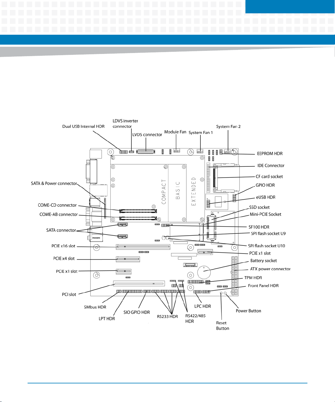
3.1 Carrier Board Layout
Figure 3-1 COMX-CAR-210 Board Layout
Chapter 3
COMX-CAR-210 Installation and Use (6806800L14D)
25
Page 26
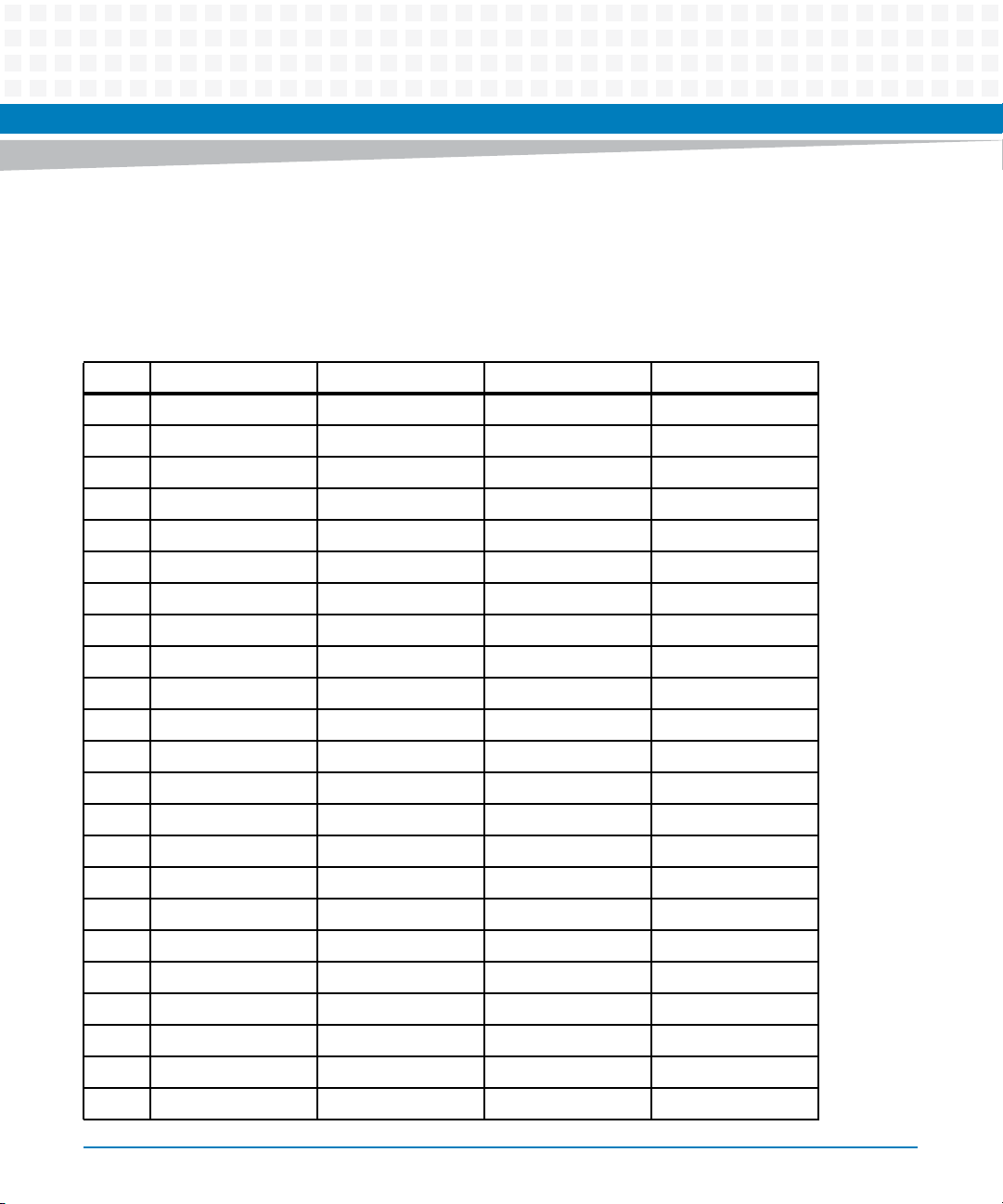
Controls, LEDs, and Connectors
3.2 COM Express Board-to-Board Connector
This section details the pin assignments on the COM Express connector based on the Type 2
specification.
Table 3-1 COM EXPRESS Connector Pin Definition
Row A B C D
1 GND (FIXED) GND (FIXED) GND (FIXED) GND (FIXED)
2 GBE0_MDI3- GBE0_ACT# IDE_D7 IDE_D5
3 GBE0_MDI3+ LPC_FRAME# IDE_D6 IDE_D10
4 GBE0_LINK100# LPC_AD0 IDE_D3 IDE_D11
5 GBE0_LINK1000# LPC_AD1 IDE_D15 IDE_D12
6 GBE0_MDI2- LPC_AD2 IDE_D8 IDE_D4
7 GBE0_MDI2+ LPC_AD3 IDE_D9 IDE_D0
8 GBE0_LINK# LPC_DRQ0# IDE_D2 IDE_REQ
9 GBE0_MDI1- LPC_DRQ1# IDE_D13 IDE_IOW#
10 GBE0_MDI1+ LPC_CLK IDE_D1 IDE_ACK#
11 GND (FIXED) GND (FIXED) GND (FIXED) GND (FIXED)
12 GBE0_MDI0- PWRBTN# IDE_D14 IDE_IRQ
13 GBE0_MDI0+ SMB_CK IDE_IORY IDE_A0
14 GBE0_CTREF SMB_DAT IDE_IOR# IDE_A1
15 SUS_S3# SMB_ALERT# PCI_PME# IDE_A2
16 SATA0_TX+ SATA1_TX+ PCI_GNT2# IDE_CS1#
17 SATA0_TX- SATA1_TX- PCI_REQ2# IDE_CS3#
18 SUS_S4# SUS_STAT# PCI_GNT1# PCI_GNT#3
19 SATA0_RX+ SATA1_RX+ PCI_REQ1# PCI_GNT3#
20 SATA0_RX- SATA1_RX- PCI_GNT0# PCI_REQ3#
21 GND (FIXED) GND (FIXED) GND (FIXED) GND (FIXED)
22 SATA2_TX+ SATA3_TX+ PCI_REQ0# PCI_AD1
23 SATA2_TX- SATA3_TX- PCI_RESET# PCI_AD3
26
COMX-CAR-210 Installation and Use (6806800L14D)
Page 27
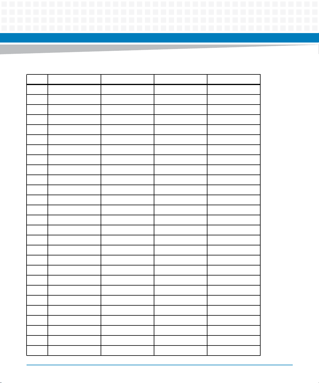
Controls, LEDs, and Connectors
Table 3-1 COM EXPRESS Connector Pin Definition (continued)
Row A B C D
24 SUS_S5# PWR_OK PCI_AD0 PCI_AD5
25 SATA2_RX+ SATA3_RX+ PCI_AD2 PCI_AD7
26 SATA2_RX- SATA3_RX- PCI_AD4 PCI_C/BE0#
27 BATLOW# WDT PCI_AD6 PCI_AD9
28 (S)ATA_ACT# NC PCI_AD8 PCI_AD11
29 AC/HDA_SYNC NC PCI_AD10 PCI_AD13
30 AC/HDA_RST# AC/HDA_SDIN0 PCI_AD12 PCI_AD15
31 GND (FIXED) GND (FIXED) GND (FIXED) GND (FIXED)
32 AC/HDA_BITCLK SPKR PCI_AD14 PCI_PAR
33 AC/HDA_SDOUT I2C_CK PCI_C/BE1# PCI_SERR
34 BIOS_DIS0# I2C_DAT PCI_PERR# PCI_STOP#
35 THRMTRIP# THRM# PCI_LOCK# PCI_TRDY#
36 USB6- USB7- PCI_DEVSEL# PCI_FRAME#
37 USB6+ USB7+ PCI_IRDY# PCI_AD16
38 USB_6_7_OC# USB_4_5_OC# PCI_C/BE2# PCI_AD18
39 USB4- USB5- PCI_AD17 PCI_AD20
40 USB4+ USB5+ PCI_AD19 PCI_AD22
41 GND (FIXED) GND (FIXED) GND (FIXED) GND (FIXED)
42 USB2- USB3- PCI_AD21 PCI_AD24
43 USB2+ USB3+ PCI_AD23 PCI_AD26
44 USB_2_3_OC# USB_0_1_OC# PCI_C/BE3# PCI_AD28
45 USB0- USB1- PCI_AD25 PCI_AD30
46 USB0+ USB1+ PCI_AD27 PCI_IRQC#
47 VCC_RTC NC PCI_AD29 PCI_IRQD#
48 EXCD0_PERST# NC PCI_AD31 PCI_CLKRUN#
49 EXCD0_CPPE# SYS_RESET# PCI_IRQA# PCI_M66EN
50 LPC_SERIRQ CB_RESET# PCI_IRQB# PCI_CLK
COMX-CAR-210 Installation and Use (6806800L14D)
27
Page 28
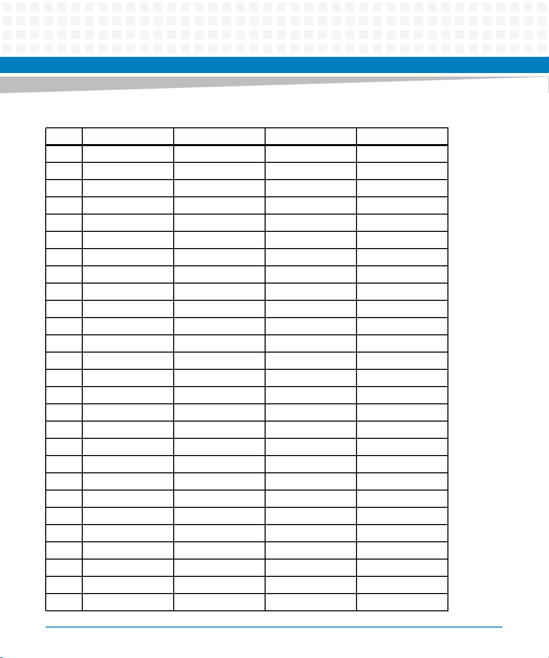
Controls, LEDs, and Connectors
Table 3-1 COM EXPRESS Connector Pin Definition (continued)
Row A B C D
51 GND (FIXED) GND (FIXED) GND (FIXED) GND (FIXED)
52 PCIE_TX5+ PCIE_RX5+ PEG_RX0+ PEG_TX0+
53 PCIE_TX5- PCIE_RX5- PEG_RX0- PEG_TX0-
54 GPI0 GPO1 TYPE0# PEG_LANE_RV#
55 PCIE_TX4+ PCIE_RX4+ PEG_RX1+ PEX_TX1+
56 PCIE_TX4- PCIE_RX4- PEG-RX1- PEX_TX1-
57 GND GPO2 TYPE1# TYPE2#
58 PCIE_TX3+ PCIE_RX3+ PEG_RX2+ PEG_TX2+
59 PCIE_TX3- PCIE_RX3- PEG_RX2- PEG_TX2-
60 GND (FIXED) GND (FIXED) GND (FIXED) GND (FIXED)
61 PCIE_TX2+ PCIE_RX2+ PEG_RX3+ PEG_TX3+
62 PCIE_TX2- PCIE_RX2- PEG_RX3- PEG_TX3-
63 GPI1 GPO3 RSVD RSVD
64 PCIE_TX1+ PCIE_RX1+ RSVD RSVD
65 PCIE_TX1- PCIE_RX1- PEG_RX4+ PEG_TX4+
66 GND WAKE0# PEG_RX4- PEG_TX4-
67 GPI2 WAKE1# FAN_PWMOUT GND
68 PCIE_TX0+ PCIE_RX0+ PEG_RX5+ PEG_TX5+
69 PCIE_TX0- PCIE_RX0- PEG_RX5- PEG_TX5-
70 GND (FIXED) GND (FIXED) GND (FIXED) GND (FIXED)
71 LVDS_A0+ LVDS_B0+ PEG_RX6+ PEG_TX6+
72 LVDS_A0- LVDS_B0- PEG_RX6- PEG_TX6-
73 LVDS_A1+ LVDS_B1+ SDVO_DATA SDVO_CLK
74 LVDS_A1- LVDS_B1- PEG_RX7+ PEG_TX7+
75 LVDS_A2+ LVDS_B2+ PEG_RX7- PEG_TX7-
76 LVDS_A2- LVDS_B2- GND GND
77 LVDS_VDD_EN LVDS_B3+ FAN_TACHOIN IDE_CBLID#
28
COMX-CAR-210 Installation and Use (6806800L14D)
Page 29
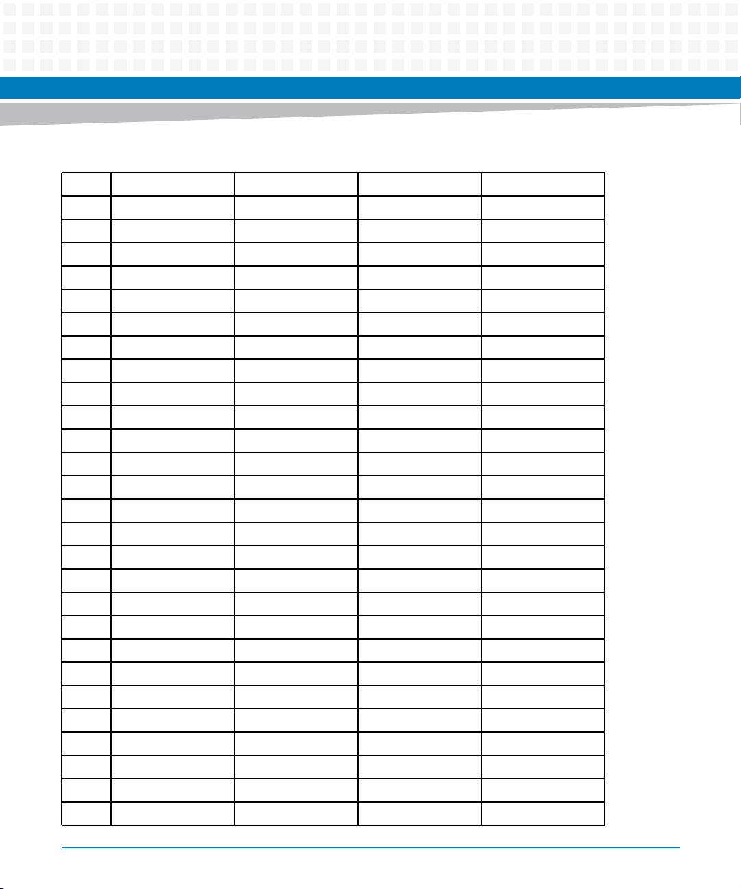
Controls, LEDs, and Connectors
Table 3-1 COM EXPRESS Connector Pin Definition (continued)
Row A B C D
78 LVDS_A3+ LVDS_B3- PEG_RX8+ PEG_TX8+
79 LVDS_A3- LVDS_BKLT_EN PEG_RX8- PEG_TX8-
80 GND (FIXED) GND (FIXED) GND (FIXED) GND (FIXED)
81 LVDS_A_CK+ LVDS_B_CK+ PEG_RX9+ PEG_TX9+
82 LVDS_A_CK- LVDS_B_CK- PEG_RX9- PEG_TX9-
83 LVDS_I2C_CK LVDS_BKLT_CTRL PP_TPM RSVD
84 LVDS_I2C_DAT VCC_5V_SBY GND GND
85 GPI3 VCC_5V_SBY PEG_RX10+ PEG_TX10+
86 KBD_RST# VCC_5V_SBY PEG_RX10- PEG_TX10-
87 KBD_A20GATE VCC_5V_SBY GND GND
88 PCIE0_CK_REF+ SPI_CS1#
10
89 PCIE0_CK_REF- VGA_RED PEG_RX11- PEG_TX11-
PEG_RX11+ PEG_TX11+
90 GND (FIXED) GND (FIXED) GND (FIXED) GND (FIXED)
91 SPI_CS0#
92 SPI_MISO
10
10
VGA_GRN PEG_RX12+ PEG_TX12+
VGA_BLU PEN_RX12- PEG_TX12-
93 GPO0 VGA_HSYNC GND GND
94 SPI_CLK
95 SPI_MOSI
10
10
VGA_VSYNC PEG_RX13+ PEG_TX13+
VGA_I2C_CK PEG_RX13- PEG_TX13-
96 GND VGA_I2C_DAT GND GND
97 VCC_12V BIOS_DIS1# RSVD PEG_ENABLE#
98 VCC_12V NC PEG_RX14+ PEG_RX14+
99 VCC_12V NC PEG_RX14- PEG_TX14-
100 GND (FIXED) GND (FIXED) GND (FIXED) GND (FIXED)
101 VCC_12V VCC_12V PEG_RX15+ PEG_TX15+
102 VCC_12V VCC_12V PEG_RX15- PEG_TX15-
103 VCC_12V VCC_12V GND GND
104 VCC_12V VCC_12V VCC_12V VCC_12V
COMX-CAR-210 Installation and Use (6806800L14D)
29
Page 30
Controls, LEDs, and Connectors
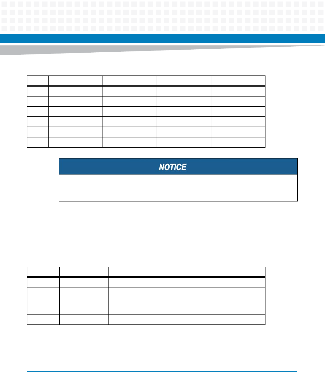
Table 3-1 COM EXPRESS Connector Pin Definition (continued)
Row A B C D
105 VCC_12V VCC_12V VCC_12V VCC_12V
106 VCC_12V VCC_12V VCC_12V VCC_12V
107 VCC_12V VCC_12V VCC_12V VCC_12V
108 VCC_12V VCC_12V VCC_12V VCC_12V
109 VCC_12V VCC_12V VCC_12V VCC_12V
110 GND (FIXED) GND (FIXED) GND (FIXED) GND (FIXED)
The signals group of PEG_TX [0:3] and PEG_RX [0:2] are routed to two PCIE Mux to switch
the signals between PEG and SDVO.
3.3 LEDs
The COMX-CAR-210 implemented some LEDs to indicate system status. The detailed function
description is listed below.
Table 3-2 LED function description
Location Status Description
D34 Type 2 Error ON: Module does not comply with Type 2 spec
D26 Thermal Trip ON: CPU is hot, system will shut down (only when the system is
running)
D21 Platform reset ON: All power is OK and system is ready to start
D28 Suspend ON: The module status is suspended
3.4 Connectors
This section lists down the information on the connectors of the COMX-CAR-210.
30
COMX-CAR-210 Installation and Use (6806800L14D)
Page 31
3.4.1 Video
3.4.1.1 LVDS
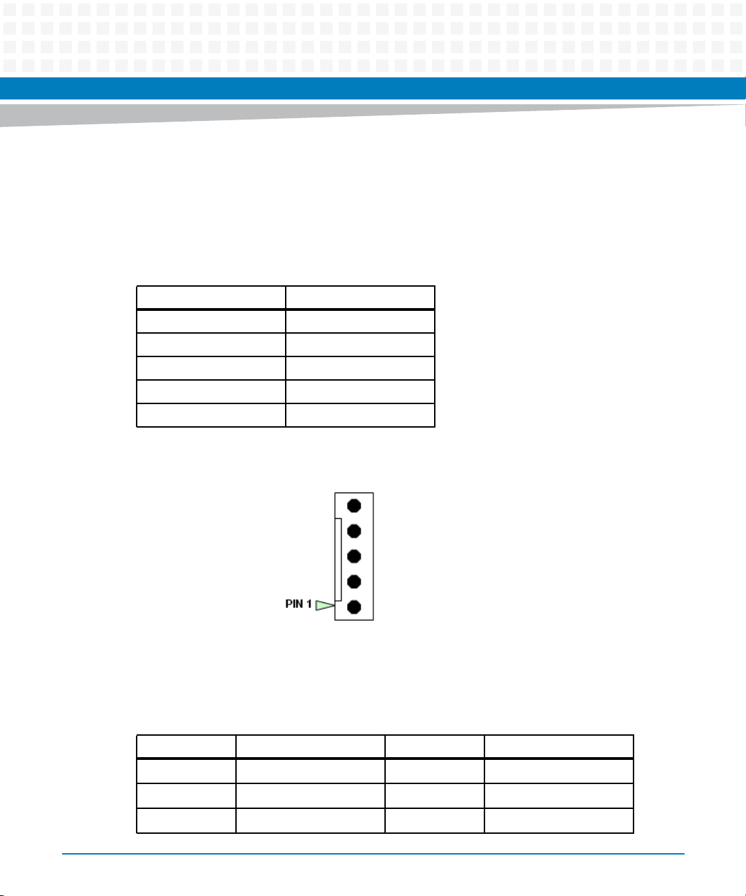
Table 3-3 P8, LVDS Inverter Header Pin-out
Pin Signal
1 12V
2 BKLT_EN
3GND
4 BKLT_CTRL
55V
Controls, LEDs, and Connectors
Figure 3-2 LVDS Inverter Header (P8)
Table 3-4 P6, LVDS Connector Pin Definition
Pin Signal Pin Signal
1 LVDSA_DATA0_P 2 LVDSB_DATA0_P
3 LVDSA_DATA0_N 4 LVDSB_DATA0_N
7 LVDSA_DATA1_P 8 LVDSB_DATA1_P
COMX-CAR-210 Installation and Use (6806800L14D)
31
Page 32
Controls, LEDs, and Connectors
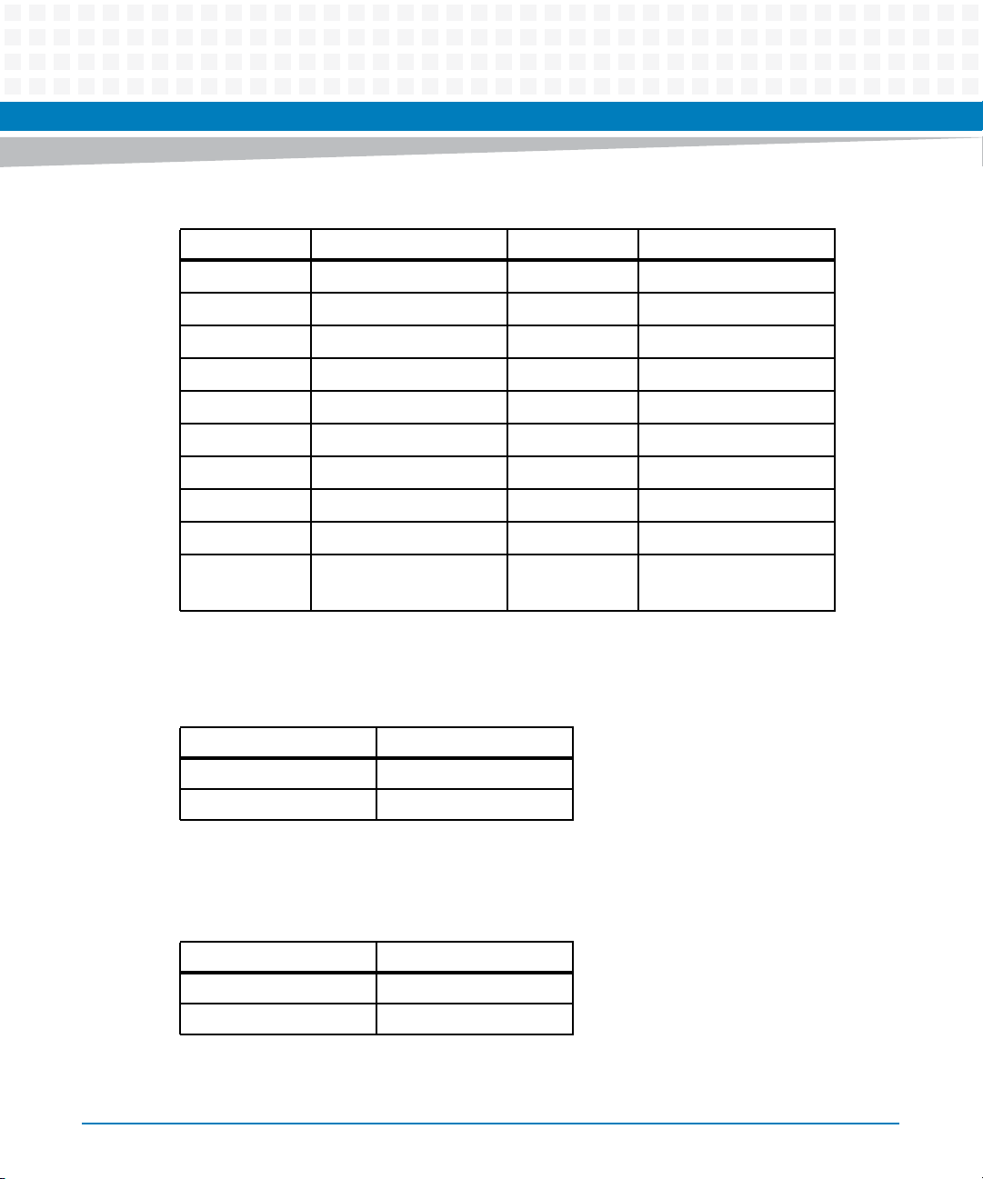
Table 3-4 P6, LVDS Connector Pin Definition (continued)
Pin Signal Pin Signal
9 LVDSA_DATA1_N 10 LVDSB_DATA1_N
13 LVDSA_DATA2_P 14 LVDSB_DATA2_P
15 LVDSA_DATA2_N 16 LVDSB_DATA2_N
19 LVDSA_DATA3_P 20 LVDSB_DATA3_P
21 LVDSA_DATA3_N 22 LVDSB_DATA3_N
25 LVDSA_CLK_P 26 LVDSB_CLK_P
27 LVDSA_CLK_N 28 LVDSB_CLK_N
31 LVDS_I2C_CLK 32 LVDS_I2C_DATA
33,35,37,39 VDD (3.3V OR 5V) 36,38,40 VDD (12V)
5,
11,17,23,29
GND 6,12,18,24,30
,34
GND
The 3V or 5V DC for the LVDS power supply is configured through the 3-pin jumper P7.
Table 3-5 P7, LVDS Power Supply Jumper Configuration
Jumper Setting Configuration
P7 (1-2) 3.3 V (Default)
P7 (2-3) 5V
The 12V DC LVDS power supply is configured through the 3-pin header P35.
Table 3-6 P35, LVDS Power Supply Jumper Configuration
Jumper Setting Configuration
P35 (1-2) Enable 12V
P35 (2-3) NC (Default)
32
COMX-CAR-210 Installation and Use (6806800L14D)
Page 33
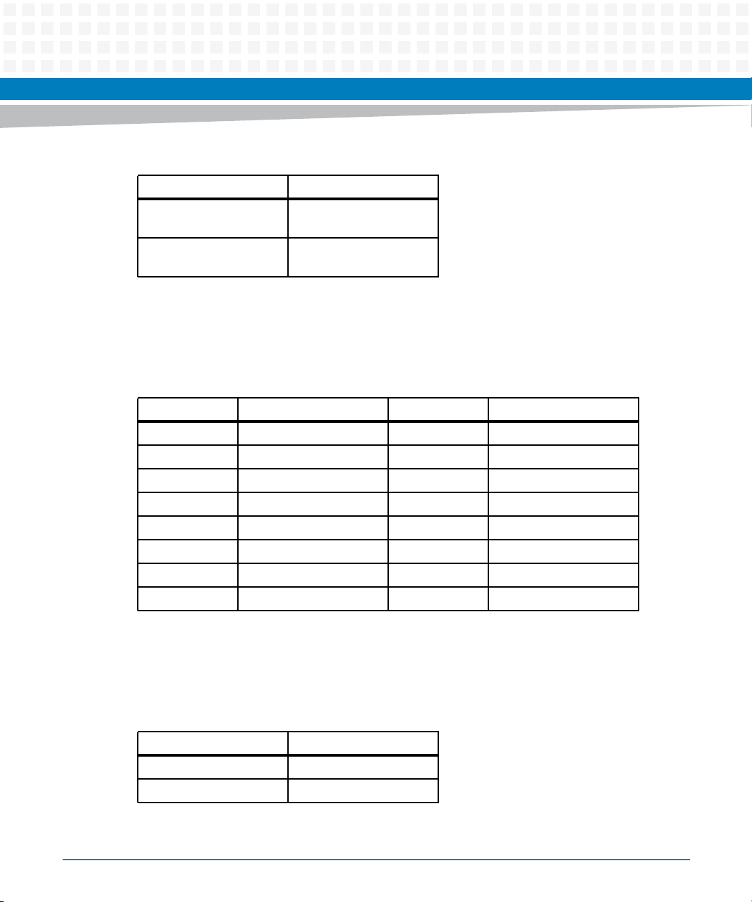
Table 3-7 P26, 5V Stand-by Jumper Setting
Jumper Setting Configuration
P26 (1-2) Enable 5V_standby to
P26 (2-3) Disable 5V_standby to
3.4.1.2 VGA
Table 3-8 J5, VGA Connector Pin-out
Pin Signal Pin Signal
1C CRT_R 2C CRT_G
Controls, LEDs, and Connectors
module (default
module
3C CRT_B 4C NC
5C GND 6C GND
7C GND 8C GND
9C 5V 10C NC
11C NC 12C DDCDATA
13C HSYNC 14C VSYNC
15C DDCCLK
3.4.1.3 SDVO to DVI
Table 3-9 P13, SDVO to DVI Jumper Setting
Jumper Setting Configuration
P13 (1-2) Switch to DVI
P13 (2-3) Switch to PEG (Default)
COMX-CAR-210 Installation and Use (6806800L14D)
33
Page 34
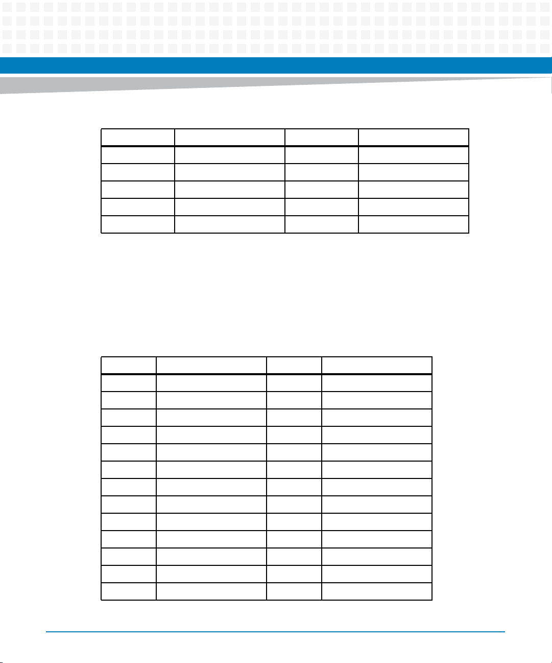
Controls, LEDs, and Connectors
Table 3-10 J5, DVI Connector Pin-out
Pin Signal Pin Signal
1A DVI_TX2_N 2A DVI_TX2_P
9A DVI_TX1_N 10A DVI_TX1_P
14A VCC5_DVI 16A DVI_PLUG_DET
17A DVI_TX0_N 18A DVI_TX0_P
23A DVI_CLK_P 24A DVI_CLK_N
3.4.2 Audio
3.4.2.1 Audio Jack
Table 3-11 J10, Audio Jack Pin-out
Pin Signal Pin Signal
1 GND 2 SIDE_L_CONN_B
3 GND 4 SIDESURR_JD_B
5 SIDE_R_CONN_B 22 SURR_L_CONN
23 GND 24 SURR_JD
25 SURR_R_CONN 32 CENTER_CONN
33 GND 34 CEN_JD
35 LFE_CONN 41 GND
42 MIC1_L_CONN 43 GND
44 MIC1_JD 45 MIC1_R_CONN
52 LOUT_L_CONN 53 GND
54 LOUT_JD 55 LOUT_R_CONN
62 LIN_L_CONN 63 GND
64 LIN_JD 65 LIN_R_CONN
34
COMX-CAR-210 Installation and Use (6806800L14D)
Page 35
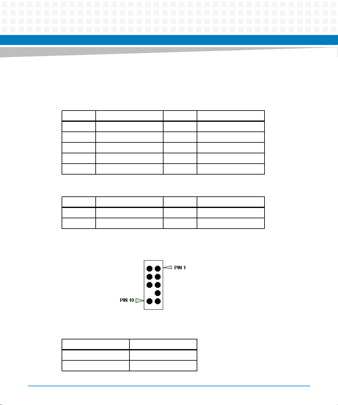
3.4.2.2 Audio Header
Table 3-12 P11, Audio Header 1 Pin-out
Pin Signal Pin Signal
1 MIC2_L 2 GND
3 MIC_2_R 4 NC
5 LOUT2_R 6 MIC2_JD
7GND 8KEY
9 LOUT2_L 10 LOUT2_JD
Table 3-13 P53, Audio Header 2 Pin-out
Controls, LEDs, and Connectors
Pin Signal Pin Signal
1 SIDE_R_CONN_H 2 SIDE_R_CONN_H
3 SIDE_R_JD_H 4 GND
Figure 3-3 HDA Audio Header (P11)
Table 3-14 P50, P51, P52 Jumper setting for side-surround output
Jumper Setting Configuration
P50, P51, P52 (1-2) Switch to rear IO (default)
P50, P51, P52 (2-3) Switch to internal header
COMX-CAR-210 Installation and Use (6806800L14D)
35
Page 36
Controls, LEDs, and Connectors
3.4.3 LAN
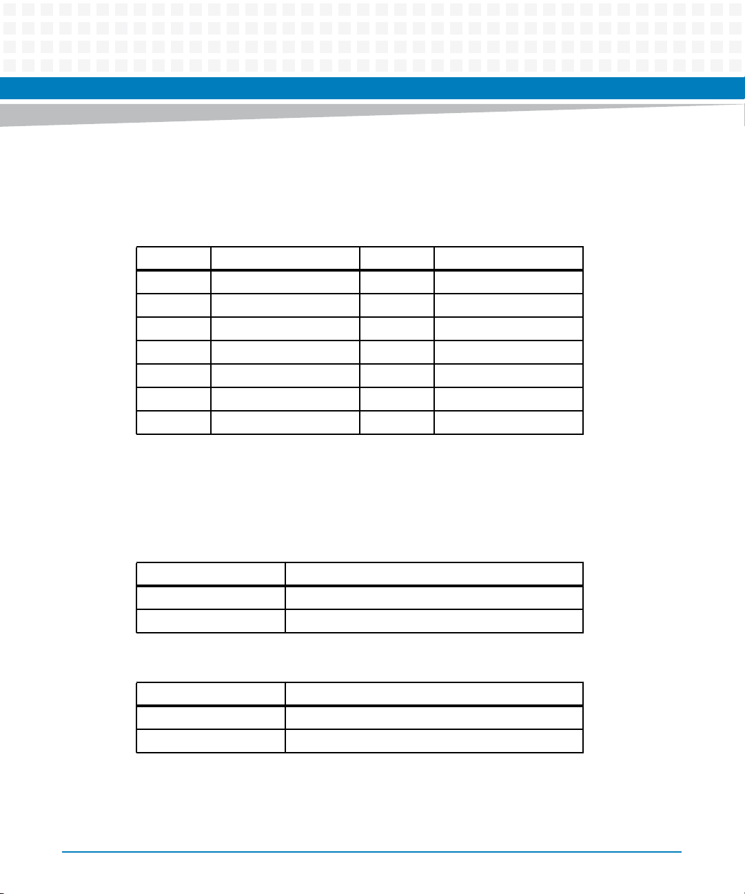
Table 3-15 J1, LAN Connectors Pin-Out
Pin Signal Pin Signal
9 GBE0_CTREF 16 LAN_MDI3_P
10 LAN_MDI0_P 17 LAN_MDI3_N
11 LAN_MDI0_N 18 GND
12 LAN_MDI1_N 19 LAN_LED_LINK1000_N
13 LAN_MDI1_N 20 LAN_LED_LINK100_N
14 LAN_MDI1_P 21 VCC3V3_DUAL
15 LAN_MDI2_N 22 LAN_LED_ACT_N
3.4.4 PCI Express
Jumpers P13 and P25 are used to configure the PCIe MUX devices.
Table 3-16 P13, PCIe MUX Configuration
Jumper Setting Configuration
P13 (1-2) SDVO Output
P13 (2-3) PEG Output (Default)
Table 3-17 P25, PCIe MUX Configuration
Jumper Setting Configuration
P25 (1-2) PCIE X1 slot (Default)
P25 (2-3) PCIE Mini-card
36
COMX-CAR-210 Installation and Use (6806800L14D)
Page 37
3.4.5 USB
3.4.5.1 USB 2.0
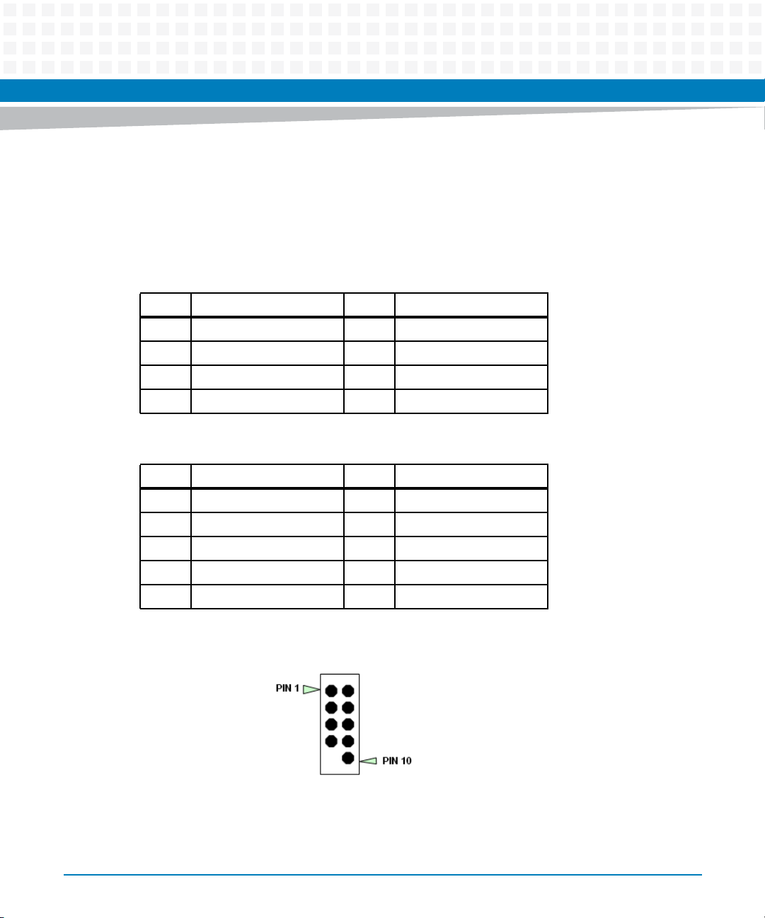
Table 3-18 J15, Dual USB 2.0 x2 ports on rear IO Pin-out
Pin Signal Pin Signal
A1 5VDUAL B1 5VDUAL
A2 USB2_N B2 USB3_N
A3 USB2_P B3 USB3_P
A4 GND B4 GND
Table 3-19 P14, One USB 2.0 Header
Controls, LEDs, and Connectors
Pin Signal Pin Signal
1 5VDUAL 2 5VDUAL
3 USB4_N 4 USB5_N
5 USB4_P 6 USB5_P
7GND 8GND
9NC 10GND
Figure 3-4 USB Header (P14, P15)
COMX-CAR-210 Installation and Use (6806800L14D)
37
Page 38
Controls, LEDs, and Connectors
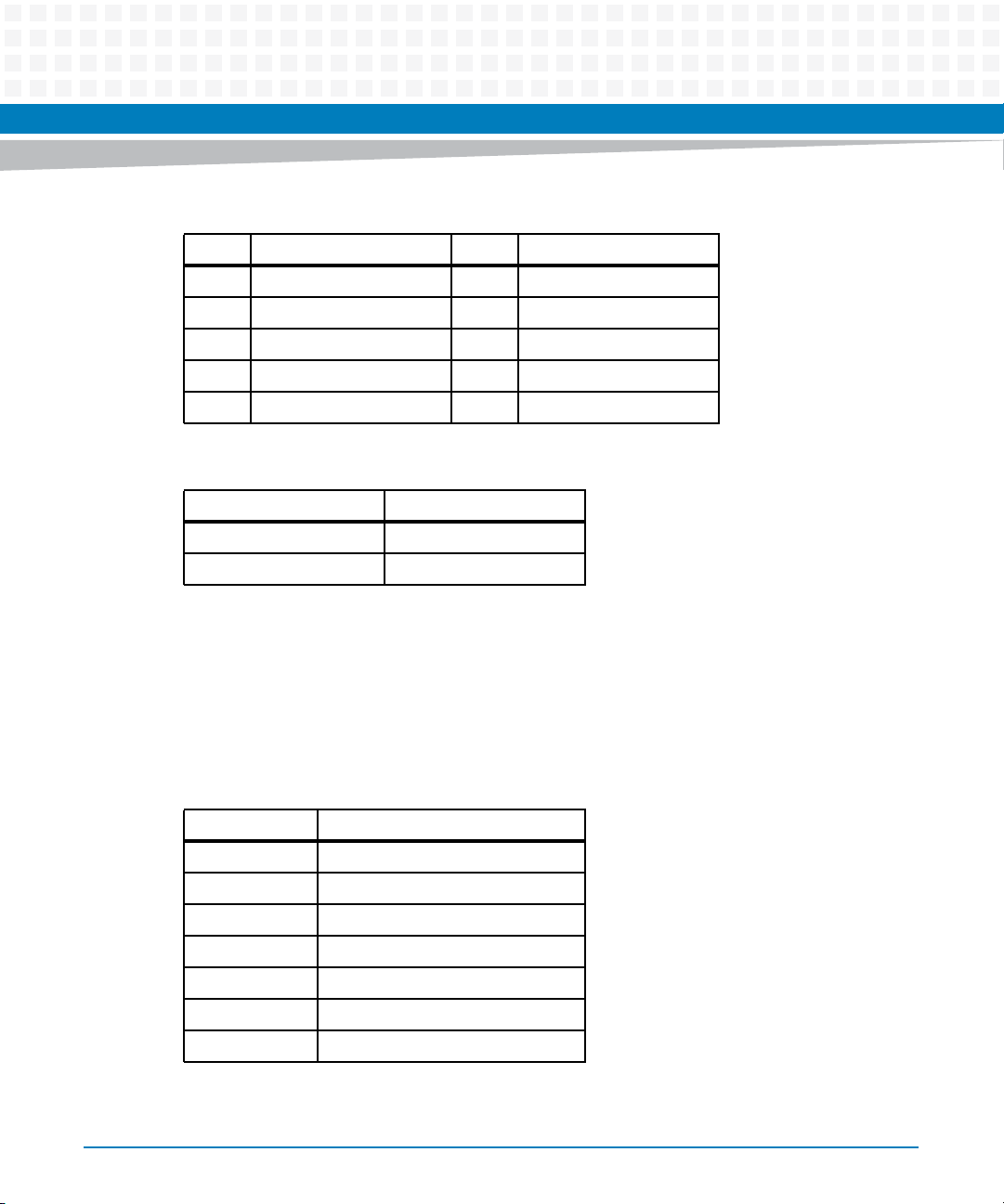
Table 3-20 P15, USB 2.0 Header for eUSB Flash
Pin Signal Pin Signal
1 5VDUAL 2 NC
3 USB6_N 4 USB7_N
5 USB6_P 6 USB7_P
7GND 8GND
9 Key 10 NC
Table 3-21 P10, USB MUX Configuration
Jumper Setting Configuration
P10 (1-2) USB 2.0 Onboard
P10 (2-3) Mini-card (Default)
3.4.6 Storage
3.4.6.1 SATA
Table 3-22 J11-J12, SATA Sockets Pin-out
Pin Signal
1GND
2 SATA_TX_P
3 SATA_TX_N
4GND
5 SATA_RX_N
6 SATA_RX_P
7GND
38
COMX-CAR-210 Installation and Use (6806800L14D)
Page 39
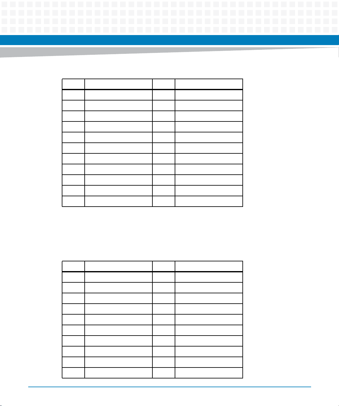
Table 3-23 P38 & J14, SATA Sockets Pin-out
Pin Signal Pin Signal
S1 GND S2 SATA_TX_P
S3 SATA_TX_N S4 GND
S5 SATA_RX_N S6 SATA_RX_P
S7 GND P1 VCC3V3
P2 VCC3V3 P3 VCC3V3
P4 GND P5 GND
P6 GND P7 VCC5V
P8 VCC5V P9 VCC5V
P10 GND P11 NC
P12 GND P13 VCC12V
P14 VCC12V P15 VCC12V
Controls, LEDs, and Connectors
3.4.6.2 IDE
Table 3-24 J7 & J14 IDE Socket Pin-out
Pin Signal Pin Signal
1 IDE_CF_RESET 2 GND
3 IDE_D<7> 4 IDE_D<8>
5 IDE_D<6> 6 IDE_D<9>
7 IDE_D<5> 8 IDE_D<10>
9 IDE_D<4> 10 IDE_D<11>
11 IDE_D<3> 12 IDE_D<12>
13 IDE_D<2> 14 IDE_D<13>
15 IDE_D<1> 16 IDE_D<14>
17 IDE_D<0> 18 IDE_D<15>
19 GND 20 NC
COMX-CAR-210 Installation and Use (6806800L14D)
39
Page 40
Controls, LEDs, and Connectors
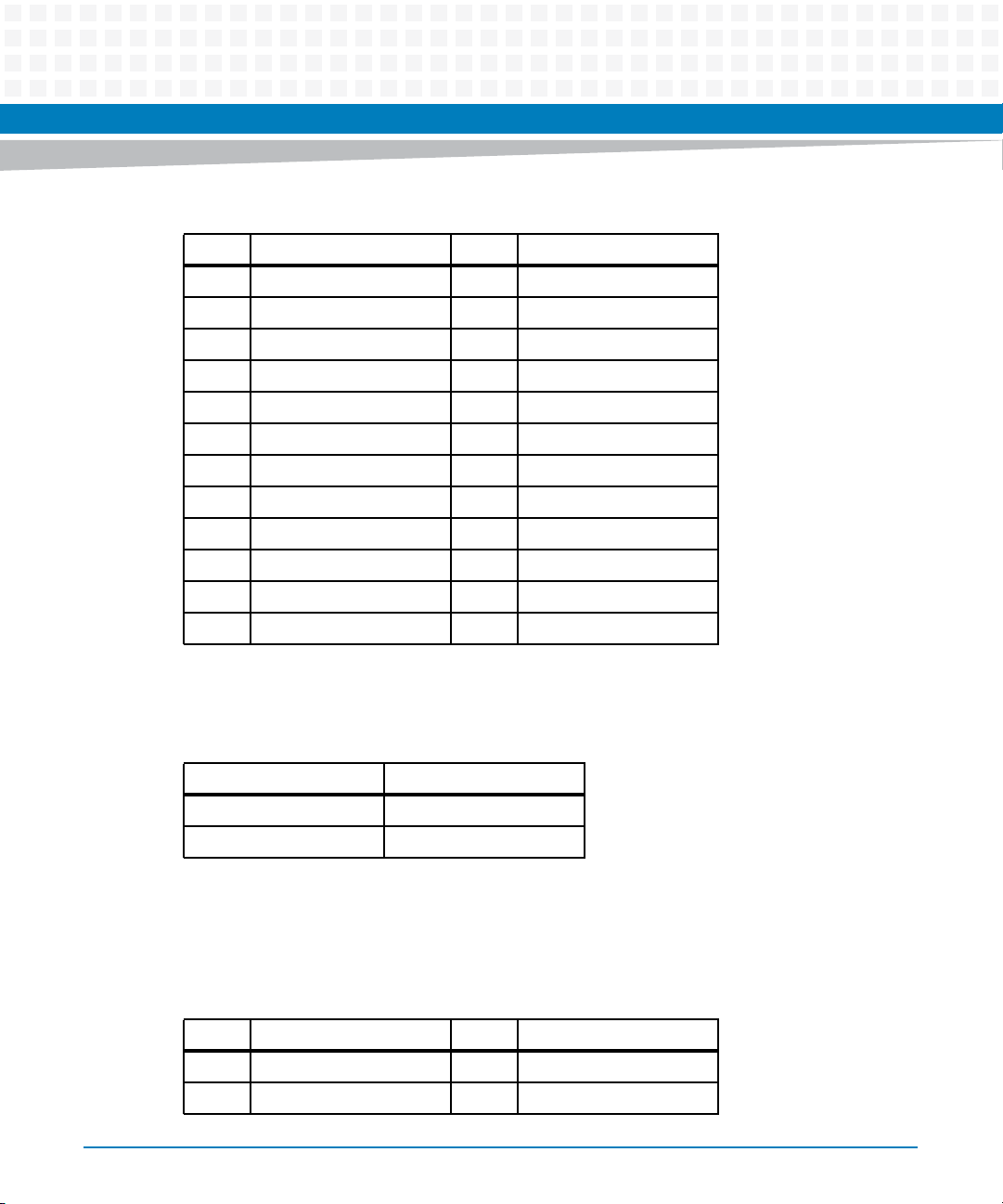
Table 3-24 J7 & J14 IDE Socket Pin-out
Pin Signal Pin Signal
21 IDE_REQ 22 GND
23 IDE_IOW_N 24 GND
25 IDE_IOR_N 26 GND
27 IDE_IORDY 28 IDE_SEL
29 IDE_ACK_N 30 GND
31 IDE_IRQ 32 NC
33 IDE_A1 34 IDE_CBLID
35 IDE_A0 36 IDE_A2
37 IDE_CS1_N 38 IDE_CS3_N
39 IDE_ACT_N 40 GND
41 VCC5V 42 VCC5V
43 GND 44 GND
Table 3-25 P39, IDE Master/Slave Jumper Setting
Jumper setting Configuration
P39 (1-2) SLAVE
P39 (2-3) Master (Default)
3.4.6.3 CF Card
Table 3-26 J7 & J14, CF Card Socket Pin-out
Pin Signal Pin Signal
1 GND 2 IDE_D<3>
3 IDE_D<4> 4 IDE_D<5>
40
COMX-CAR-210 Installation and Use (6806800L14D)
Page 41
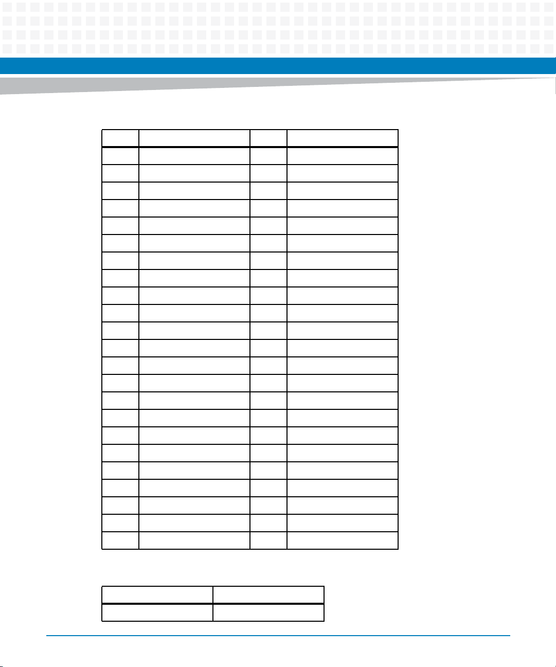
Table 3-26 J7 & J14, CF Card Socket Pin-out (continued)
Pin Signal Pin Signal
5 IDE_D<6> 6 IDE_D<7>
7 IDE_CS1_N 8 GND
9 GND 10 GND
11 GND 12 GND
13 VCC5V 14 GND
15 GND 16 GND
17 GND 18 IDE_A2
19 IDE_A1 20 IDE_A0
21 IDE_D<0> 22 IDE_D<1>
23 IDE_D<2> 24 NC
25 CF_CD2_N 26 CF_CD1_N
Controls, LEDs, and Connectors
27 IDE_D<11> 28 IDE_D<12>
29 IDE_D<13> 30 IDE_D<14>
31 IDE_D<15> 32 IDE_CS3_N
33 NC 34 IDE_IOR_N
35 IDE_IOW_N 36 CF_WE_N
37 IDE_IRQ 38 VCC5V
39 CF_MASTER_SLAVE_SEL 40 NC
41 IDE_CF_RESET 42 IDE_IORDY
43 IDE_REQ 44 IDE_ACK_N
45 CF_ACT_N 46 IDE_CBLID
47 IDE_D<8> 48 IDE_D<9>
49 IDE_D<10> 50 GND
Table 3-27 P9, CF Card Master/Slave Jumper Settings
Jumper Setting Configuration
P9 (1-2) SLAVE (Default)
COMX-CAR-210 Installation and Use (6806800L14D)
41
Page 42
Controls, LEDs, and Connectors
Table 3-27 P9, CF Card Master/Slave Jumper Settings
Jumper Setting Configuration
P9 (2-3) Master
3.4.7 Super I/O
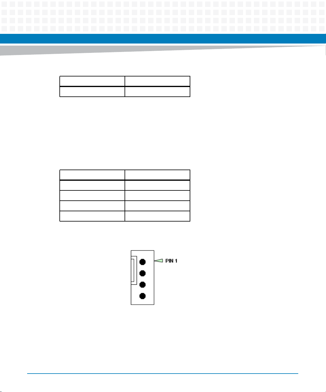
3.4.7.1 Fan
Table 3-28 P3, P42, P27, System and Module Fan Headers Pin-out
Pin Signal
1GND
2 12V
3TACH
4 PWM
Figure 3-5 FAN Connector (P3, P27, P42)
42
COMX-CAR-210 Installation and Use (6806800L14D)
Page 43
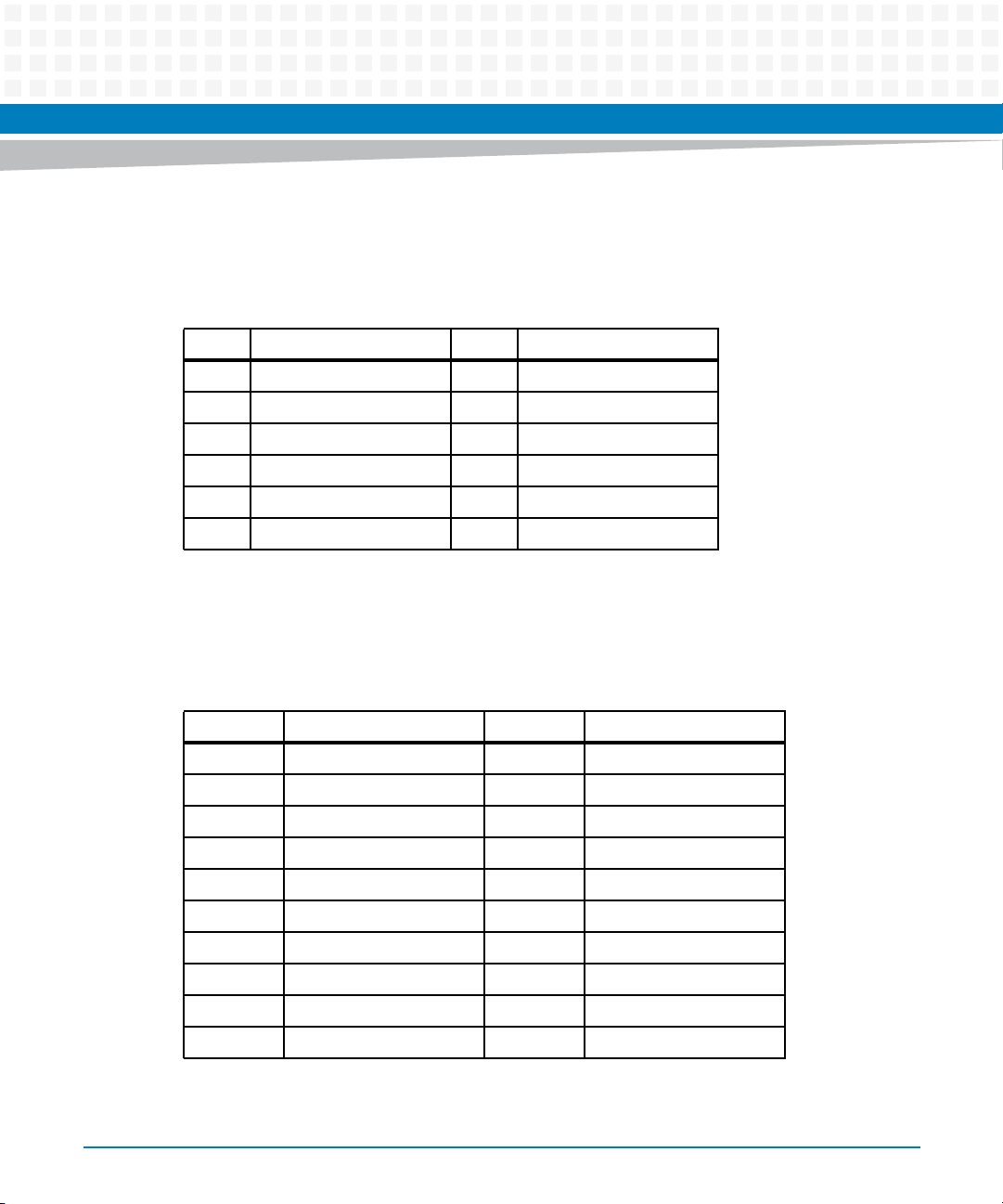
3.4.7.2 PS/2
Table 3-29 J13, PS/2 Connector Pin-Out
Pin Signal Pin Signal
1 KB_DATA 2 NC
3 GND 4 VCC5V_DUAL
5 KB_CLK 6 NC
7 MS_DATA 8 NC
9 GND 10 VCC5V_DUAL
11 MS_CLK 12 NC
3.4.7.3 LPT Port
Controls, LEDs, and Connectors
Table 3-30 P32 LPT Header Pin-out
Pin Signal Pin Signal
1 STB_N 2 PD0
3PD1 4PD2
5PD3 6PD4
7PD5 8PD6
9 PD7 10 ACK_N
11 BUSY_N 12 PE_N
13 SLCT_N 14 AFD_N
15 ERR_N 16 INIT_N
17 SLIN_N 18~25 GND
26 Key
COMX-CAR-210 Installation and Use (6806800L14D)
43
Page 44
Controls, LEDs, and Connectors
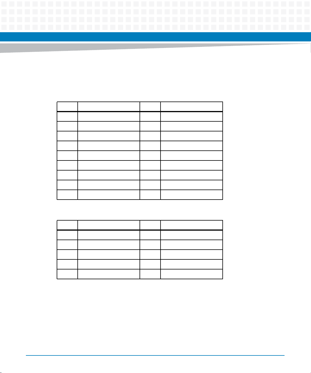
3.4.7.4 Serial Ports
Table 3-31 P5, Dual Rear IO RS232 Ports Pin-out
Pin Signal Pin Signal
A1 DCD1_N B1 DCD2_N
A2 RXD1 B2 RXD2
A3 TXD1 B3 TXD2
A4 DTR1 B4 DTR2
A5 GND B5 GND
A6 DSR1_N B6 DSR2_N
A7 RTS1_N B7 RTS2_N
A8 CTS1_N B8 CTS2_N
44
A9 RI1_N B9 RI2_N
Table 3-32 P20, P21, P22, P23 RS232 Headers Pin-Out
Pin Signal Pin Signal
1 DCD_N 2 DSR_N
3 RXD 4 RTS_N
5 TXD 6 CTS_N
7 DTR 8 RI_N
9 GND 10 NC
COMX-CAR-210 Installation and Use (6806800L14D)
Page 45
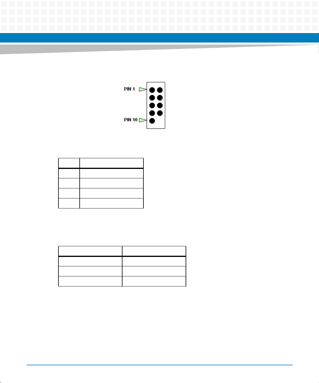
Figure 3-6 Serial port header (P20, P21, P22, P23)
Table 3-33 P37, P33, RS422/485 Headers Pin-Out
Pin Signal
1 RS422_RX_N
2 RS422_RX_P
Controls, LEDs, and Connectors
3 RS422_TX_N/RS485_N
4 RS422_TX_P/RS485_P
Table 3-34 P34, P41, PS232, RS422/485 Ports Configuration
Jumper setting Configuration
P34,P41 (1-2) RS232 (Default)
P34,P41 (3-4) RS422
P34,P41 (5-6) RS485
COMX-CAR-210 Installation and Use (6806800L14D)
45
Page 46
Controls, LEDs, and Connectors
3.5 Headers
3.5.1 Low Pin Count
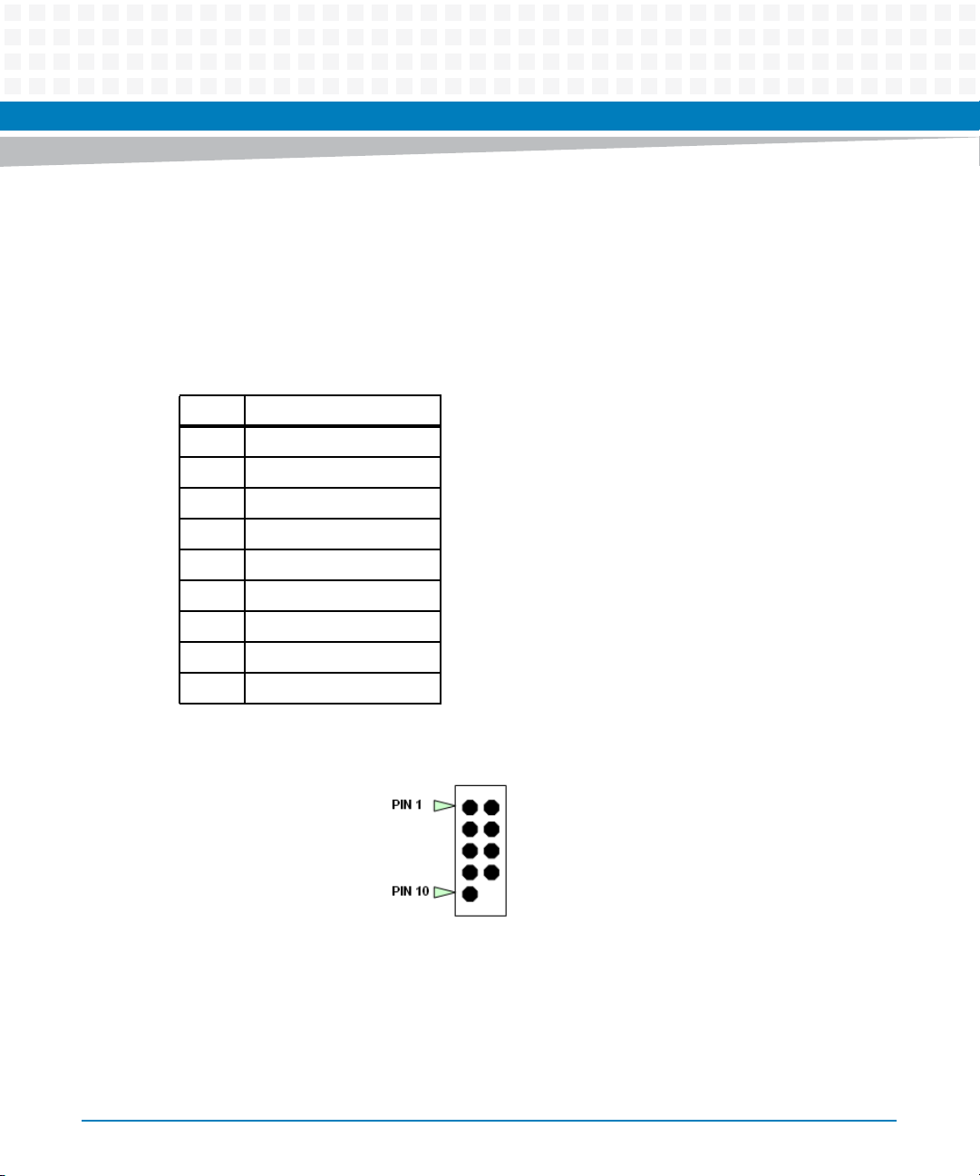
The COMX-CAR-210 supports extended Low Pin Count bus by supplying a 2 x 5 pin header.
Table 3-35 P29, Low Pin Count Header Pin-out
Pin Signal
1 CLK_33M
2 AD1
3 RST_N
4 AD0
5 FRAME_N
6 3.3V
7 AD3
8GND
9 AD2
Figure 3-7 LPC Header (P29)
46
COMX-CAR-210 Installation and Use (6806800L14D)
Page 47
3.5.2 Trusted Platform Module
Table 3-36 P28 Trust Platform Module Header Pin-out
Pin Signal Pin Signal
1 CLK_33M 2 GND
3 FRAME_N 4 NC
5RST_N 65V
7 AD3 8 AD2
9 3.3V 10 AD1
11 AD0 12 GND
13 SMB_CLK 14 SMB_DATA
Controls, LEDs, and Connectors
15 3VDUAL 16 INT_SERIRQ
17 GND 18 CLKRUN_N
19 3.3V 20 DRQ0_N
3.5.3 GPIO
Table 3-37 P30 Module GPIO Header Pin-Out
Pin Signal
1GPO0
2GPI0
3GPO1
4GPI1
5GPO2
6GPI2
7GPO3
COMX-CAR-210 Installation and Use (6806800L14D)
47
Page 48
Controls, LEDs, and Connectors
Table 3-37 P30 Module GPIO Header Pin-Out (continued)
Pin Signal
8GPI3
9 3.3V
10 GND
Table 3-38 P19, SIO GPIO Header Pin-Out
Pin Signal
1 SIO_GPIO63
2 SIO_GPIO62
3 SIO_GPIO61
4 SIO_GPIO60
5 SIO_GPIO22
6 SIO_GPIO23
7 SIO_GPIO24
8 SIO_GPIO27
9 3.3V
10 GND
3.5.4 SMBus
Table 3-39 P18, SMBus Header Pin-out
Pin Signal
1 VCC3V3
2 SMB_CLK
3 SMB_DATA
4GND
48
COMX-CAR-210 Installation and Use (6806800L14D)
Page 49
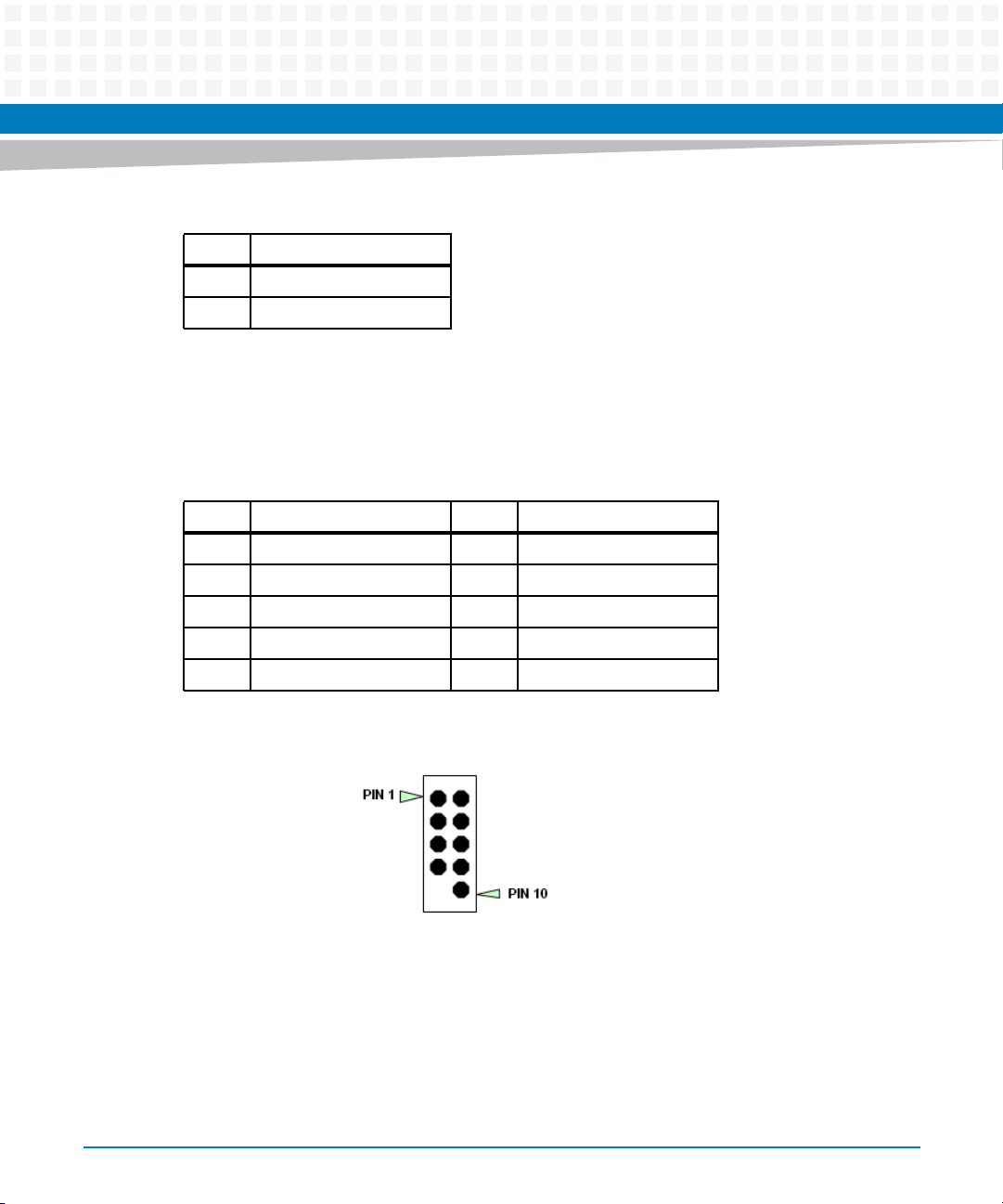
Table 3-39 P18, SMBus Header Pin-out (continued)
Pin Signal
5NC
6NC
3.5.5 Miscellaneous I/O
Table 3-40 P16, Miscellaneous I/O Header Pin-out
Pin Signal Pin Signal
1 HD_LED 2 POWER_LED
3 HD_LED# 4 POWER_LED#
Controls, LEDs, and Connectors
5 GND 6 EXT_PWRBTN_N
7 PM_SYSRST_N 8 GND
9 Key 10 NC
Figure 3-8 Front Panel Header (P16)
COMX-CAR-210 Installation and Use (6806800L14D)
49
Page 50
Controls, LEDs, and Connectors
3.5.6 SPI Flash
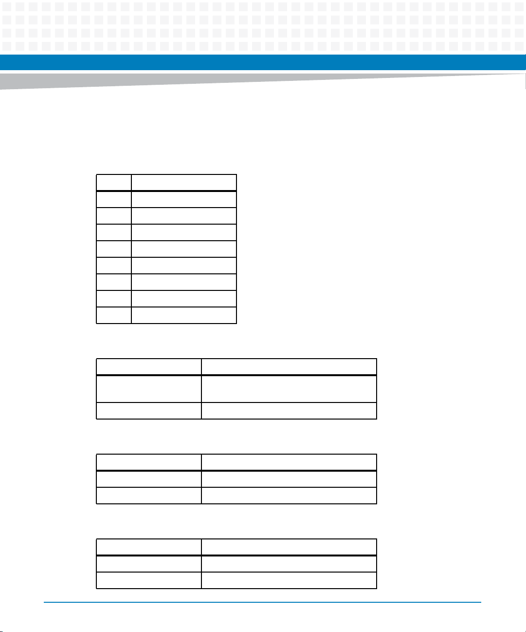
Table 3-41 P47, SF100 Header Pin-out
Pin Signal
1 3.3V
2GND
3 SPI_CS_N
4 SF_SPI_CLK
5 SF_SPI_SO
6 SF_SPI_SI
7NC
8NC
Table 3-42 P46, SPI Flash Configuration
Jumper setting Configuration
P46 (1-2) Enable SPI flash chip U9 and disable U10
(Default)
P46 (2-3 ) Enable SPI flash chip U10 and disable U9
Table 3-43 P12, BIOS Configuration on the module
Jumper setting Configuration
P12 (1-2) Enable CS0 of BIOS on the Module (Default)
P12 (2-3) Disable CS0 of BIOS on the Module
Table 3-44 P43, BIOS Configuration on the module
Jumper setting Configuration
P43 (1-2) Enable CS1 of BIOS on the Module (Default)
P43 (2-3) Disable CS1 of BIOS on the Module
50
COMX-CAR-210 Installation and Use (6806800L14D)
Page 51
3.5.7 EEPPROM
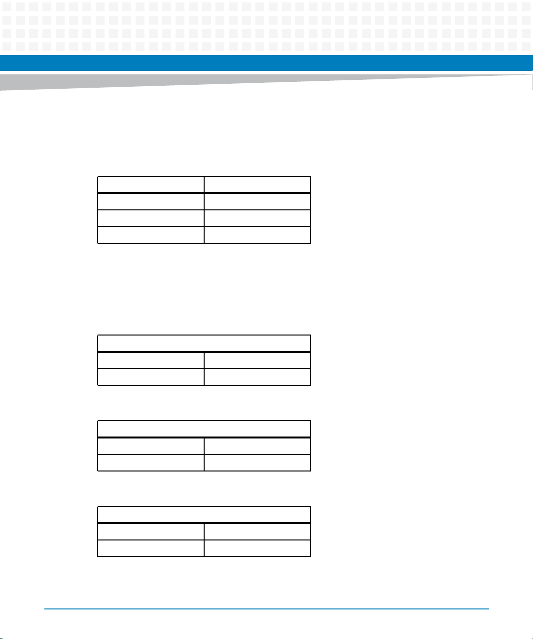
Table 3-45 P45, EEPROM Header Pin-out
Pin Signal
1 I2C_DATA
2GND
3 I2C_CLK
3.5.8 Jumper Setting Description
Controls, LEDs, and Connectors
Table 3-46 P36 PEG Enable
P36 PEG Enable
1-2 DIS PEG (Default)
2-3 Enable PEG
Table 3-47 P7 LVDS PWR1 Set
P7 LVDS PWR1 Set
1-2 3.3V (Default)
2-3 5V
Table 3-48 P25 PCIE Switch
P25 PCIE Switch
1-2 J3 PCIE X1 (Default)
2-3 Mini Card
COMX-CAR-210 Installation and Use (6806800L14D)
51
Page 52
Controls, LEDs, and Connectors
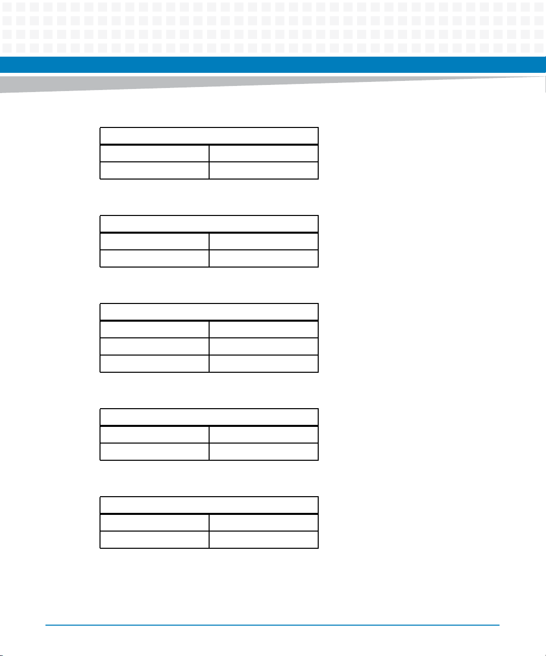
Table 3-49 P17 Case Open
P17 Case Open
1-2 Disbale (Default)
2-3 Enable
Table 3-50 P43 SPI1 Boot Sel
P43 SPI1 Boot Sel
1-2 Module (Default)
2-3 Carrier
Table 3-51 P41 COM6 Mode Sel
P41 COM6 Mode Sel
1-2 RS232 (Default)
3-4 RS422
5-6 RS485
Table 3-52 P39 IDE Master/Slave Set
P39 IDE Master/Slave Set
1-2 Slave
2-3 Master (Default)
Table 3-53 P35 LVDS PWR2 Set
P35 LVDS PWR2 Set
1-2 12V
2-3 NC (Default)
52
COMX-CAR-210 Installation and Use (6806800L14D)
Page 53
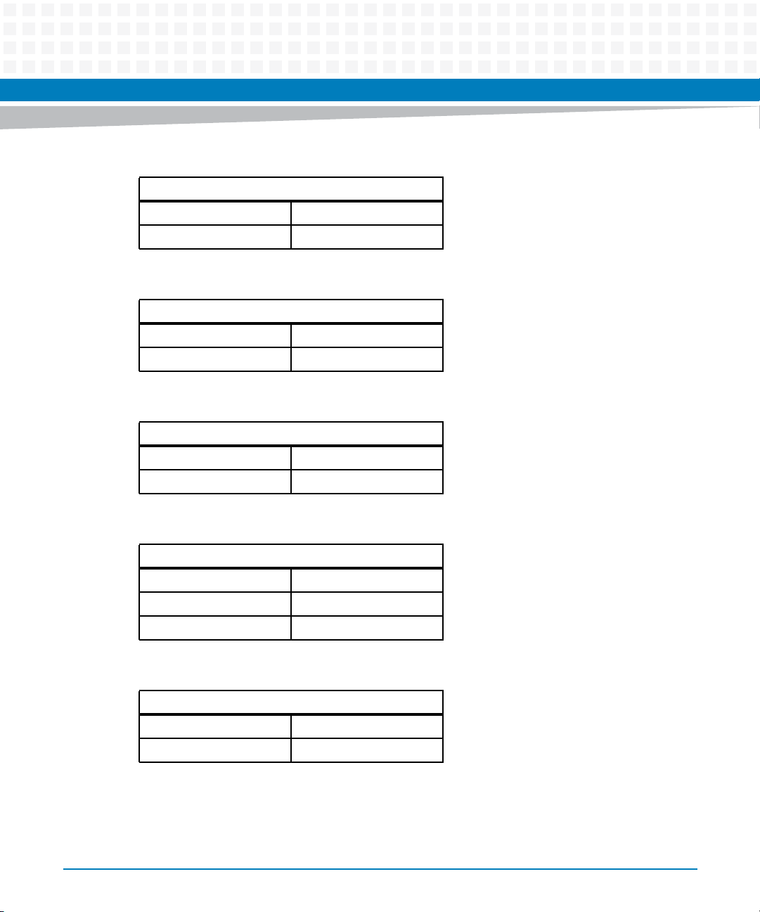
Table 3-54 P13 SDVO Switch
P13 SDVO Switch
1-2 SDVO Output
2-3 PEG Output (Default)
Table 3-55 P46 SF100 PROG PART SEL
P46 SF100 PROG PART SEL
1-2 U9 (Default)
2-3 U10
Table 3-56 P40 PS ON SEL
P40 PS ON SEL
Controls, LEDs, and Connectors
1-2 Thru SIO (Default)
2-3 S3 AND TYPE
Table 3-57 P34 COMS Mode Sel
P34 COMS Mode Sel
1-2 RS232 (Default)
3-4 RS422
5-6 RS485
Table 3-58 P9 CF Card Master/Slave
P9 CF Card Master/Slave
1-2 Slave (Default)
2-3 Master
COMX-CAR-210 Installation and Use (6806800L14D)
53
Page 54
Controls, LEDs, and Connectors
Table 3-59 P10 USB Switch
P10 USB Switch
1-2 P15 USB HDR
2-3 Mini Card (Default)
Table 3-60 P50, P51, P52 Stereo Speaker
P50, P51, P52 Stereo Speaker
1-2 Rear IO (Default)
2-3 P53 Output
Table 3-61 P12 SPI0 Boot Select
P12 SPI0 Boot Select
1-2 Module (Default)
2-3 Carrier
Table 3-62 P26 Module STB PWR SEL
P26 Module STB PWR SEL
1-2 IN (Default)
2-3 NC
Do not change the default setting of the P24 (2-3). This jumper is only for the power mode
debug usage.
54
COMX-CAR-210 Installation and Use (6806800L14D)
Page 55
Functional Description
4.1 Block Diagram
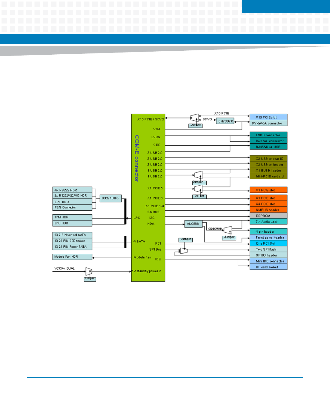
Figure 4-1 Carrier Board Block Diagram
Chapter 4
4.2 Video
The COMX-CAR-210 supports the following graphic interfaces:
4.2.1 LVDS
The graphic controller supports dual channel LVDS and up to 24-bit colors per channel.
COMX-CAR-210 Installation and Use (6806800L14D)
55
Page 56

Functional Description
The board provides an LVDS and backlight headers. The LVDS header is a 40-pin, dual-row
header, while the backlight is a 5-pin wafer header.
For information on pin assignements, see LV DS on page 31
4.2.2 VGA
The carrier board supports VGA output from the COM Express connector.
For information on pin assignments, see Table "J5, VGA Connector Pin-out" on page 33
4.2.3 SDVO to DVI
The carrier board supports both PEG and SDVO functions. It has a jumper that can choose the
signal output from the COME connector.
For information on pin assignments, seeTable "J5, DVI Connector Pin-out" on page 34
4.3 Audio
4.3.1 Audio Jack
The COMX-CAR-210 supports line output, microphone, input, line input, side surround
output, center & left, surrounding output using industry standard 7.1 channel audio-jack
connectors.
For information on pin assignments, see Table "J10, Audio Jack Pin-out" on page 34.
4.3.2 Audio Header
The board provides two internal audio headers to support the following functions:
microphone input, stereo headphone output and stereo speaker output.
56
COMX-CAR-210 Installation and Use (6806800L14D)
Page 57
Functional Description
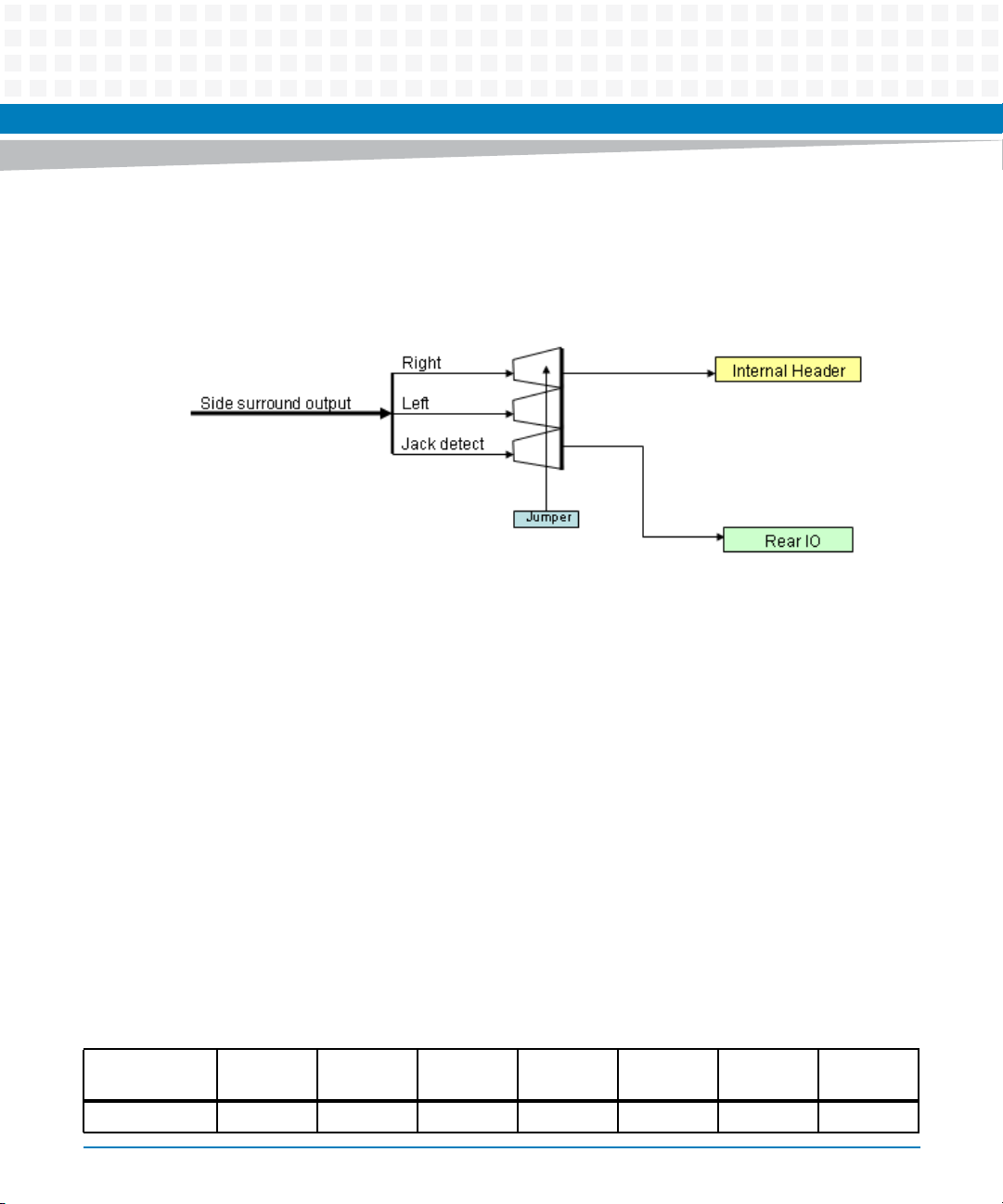
The carrier also utilizes a group of jumpers In order to support both stereo headphone output
and stereo output functions.
Figure 4-2 Side surround output switch
For information on pin-outs, see Table "P11, Audio Header 1 Pin-out" on page 35 and Table
"P53, Audio Header 2 Pin-out" on page 35.
4.4 LAN
The COMX-CAR-210 has one Gbe port. The MDI signals are directly routed from the COME
module to the RJ45 connector.
For information on pin assisgnments, see Table "J1, LAN Connectors Pin-Out" on page 36.
4.5 PCI
The COMX-CAR-210 supports a PCI slot in the PCI resource of the module.
Table 4-1 PCI Resource Table
COME Connector IRQ A IRQ B IRQ C IRQ D AD<20> PCI_REQ0 PCI_GNT0
PCI Slot INTA INTB INTC INTD IDSEL REQ0 GNT0
COMX-CAR-210 Installation and Use (6806800L14D)
57
Page 58
Functional Description
4.6 PCI Express
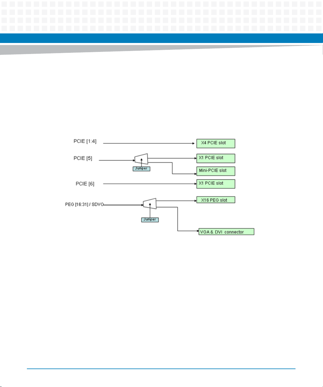
The COMX-CAR-210 has defined six groups of PCIe x1 signals. All of these signals should be
routed to the slots or devices. The lanes 1-4 are x4 PCIE slot. The lane 5 is multiplexed as a PCIe
x1 slot and a PCIe mini-card slot. The lane 6 is routed to an optional x1 slot, which is placed on
the opposite side of the rear IO. It can be described by the following block diagram.
Figure 4-3 PCI Express block diagram
58
The design also provides one x16 PCIe slot which can be used for PEG. The PEG signal lane is
multiplexed with the SDVO signals.
For information on jumper settings, see Table "P13, PCIe MUX Configuration" on page 36 and
Table "P25, PCIe MUX Configuration" on page 36.
COMX-CAR-210 Installation and Use (6806800L14D)
Page 59
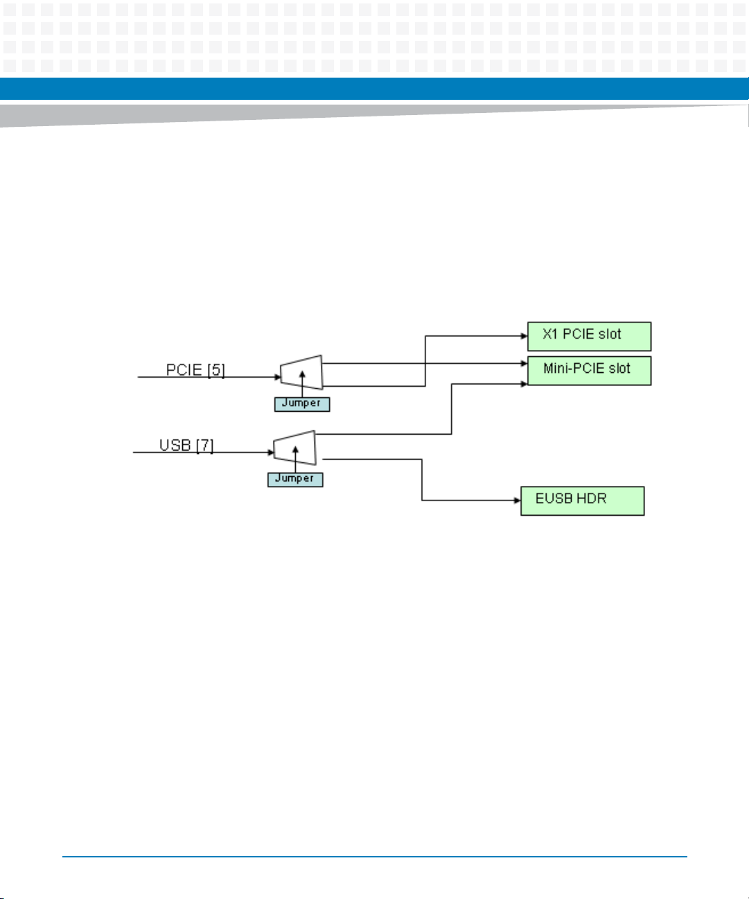
4.6.1 PCIe Mini-Card for WiFi/WiMAX
The COMX-CAR-210 has a PCI Express Mini-Card connector that conforms to and supports PCI
Express Mini-Card Electromechanical Specification 1.1 wireless devices, such as the Intel®
WiMAX/WiFi Link 5050 and the Intel® WiFi Link 5000 series, implementing both PCI Express
and USB interfaces.
Figure 4-4 PCIe Mini-Card Setting
Functional Description
4.7 USB
There are eight USB 2.0 ports on the board. Four of them are on the rear IO port, with one fixed
port for the eUSB flash and another that switches between the Mini-Card and eUSB flash header
through a USB MUX device. The next two ports are on a nine-pin header and all support lowspeed, full-speed, and high-spreed transfer rates using the USB 2.0 Enhanced Host Controller
Interface (EHCI).
For information on pin assignments, see Chapter 3, USB, on page 37.
4.8 Storage
The COMX-CAR-210 supports the following storage media: SATA, IDE and CF Card.
COMX-CAR-210 Installation and Use (6806800L14D)
59
Page 60
Functional Description
4.8.1 SATA
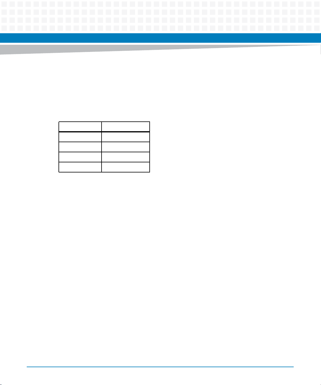
The board supports four SATA ports. Two seven pin vertical headers, one SATA port with rightangle 22-pin Power Data connector that supports a JEDEC MO-297A Slim-Lite, and one 22-pin
standard vertical power plus SATA connector.
The following table describes the group signals used by each pin.
Pin Group signals
j14 SATA0
J11 SATA1
J12 SATA2
P38 SATA3
For more information, see Chapter 3, SATA, on page 38
4.8.2 IDE
The board provides a 44-pin mini-IDE socket and a jumper to set the Master/Slave mode.
For information on the pin assignment and jumper settings, see Chapter 3, IDE, on page 39
4.8.3 CF Card
The board provides a CF card socket which can support both Type I and Type II cards.
For information on the pin assignment and jumper settings, see Chapter 3, CF Card, on page 40.
4.9 Super I/O
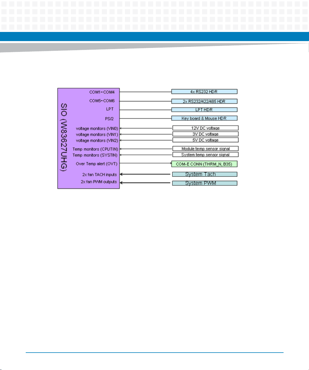
The COMX-CAR-210 provides a Super I/O for extending several function modules.
60
COMX-CAR-210 Installation and Use (6806800L14D)
Page 61
Functional Description
For information on pin assignments, see Chapter 3, Super I/O, on page 42.
Figure 4-5 Super I/O Block Diagram
4.9.1 Voltage and Thermal Monitoring
The COMX-CAR-210 provides voltage monitoring capabilities on 3 V, 5 V, and 12 V rails, and
also provides thermal monitoring capabilities for the COM Express module and its
environment.
4.9.2 Fan Control
There are three 4-wire fan headers on the COMX-CAR-210 for module fan and system fan. Fans
support fan TACH input and PWN fan speed control. The board uses a 4-pin locking connector
equivalent to the Molex 47053-1000.
For information on pin assignments, see Table "P3, P42, P27, System and Module Fan Headers
Pin-out" on page 42.
4.9.3 PS/2
The COMX-CAR-210 has one rear I/O PS/2 connector for the keyboard and mouse.
COMX-CAR-210 Installation and Use (6806800L14D)
61
Page 62

Functional Description
For information on pin assignments, see Table "J13, PS/2 Connector Pin-Out" on page 43
4.9.4 LPT
There is a 2 x 13 pin header for the LPT interface of the COMX-CAR-210.
For information on the pin assignments, see Table "P32 LPT Header Pin-out" on page 43
4.9.5 RS-232 and RS-422/485 Ports
The COMX-CAR-210 implements up to six serial ports, all default as RS-232, two of which can
be switched to RS-422 or RS-485 ports by setting two jumpers on the 2 x 3 pin header. Two RS232 ports are on the rear IO; the other two RS-232 ports are implemented as 2 x 5 pin, dualrow headers.
For information on pin-assignments, see Table "P20, P21, P22, P23 RS232 Headers Pin-Out" on
page 44 and Table "P37, P33, RS422/485 Headers Pin-Out" on page 45.
62
COMX-CAR-210 Installation and Use (6806800L14D)
Page 63
4.10 SPI Flash
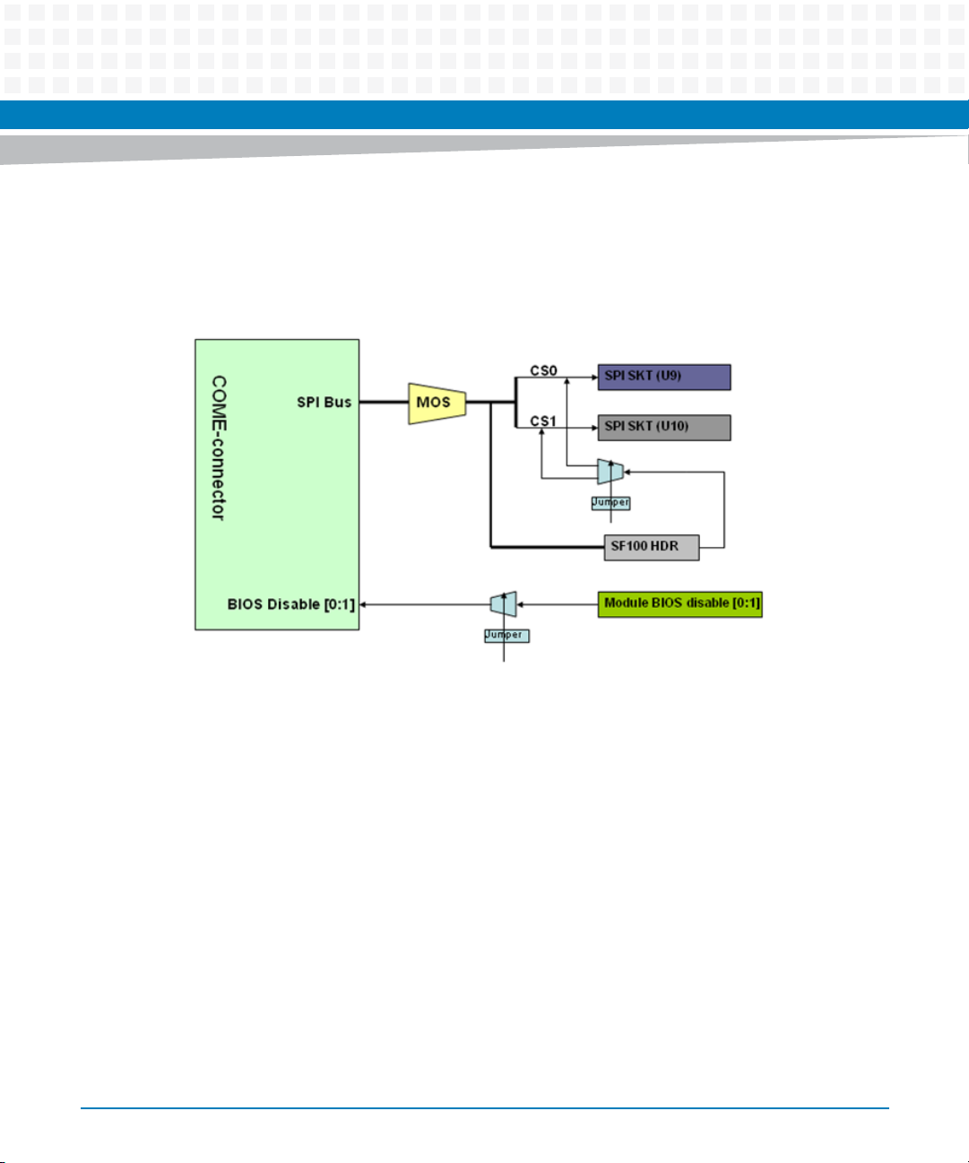
There are two SPI flash headers.
Figure 4-6 SPI Flash Block Diagram
Functional Description
The chips can be accessed through a 2x4-pin SP100 header, either by chipset or external
devices with SPI interface .
When using the SF100 on board program function, the AC power of the system should be fully
cut to avoid damage to the module. A 3-pin jumper (P46) is supplied to configure which SPI
flash will be programmed. The chip select signal from the Module CS0# is routed to the U9 and
the CS1# is routed to the U10. For information on pin assignments, see Table "P46, SPI Flash
Configuration" on page 50
COMX-CAR-210 Installation and Use (6806800L14D)
63
Page 64
Functional Description
4.11 Watchdog Timer
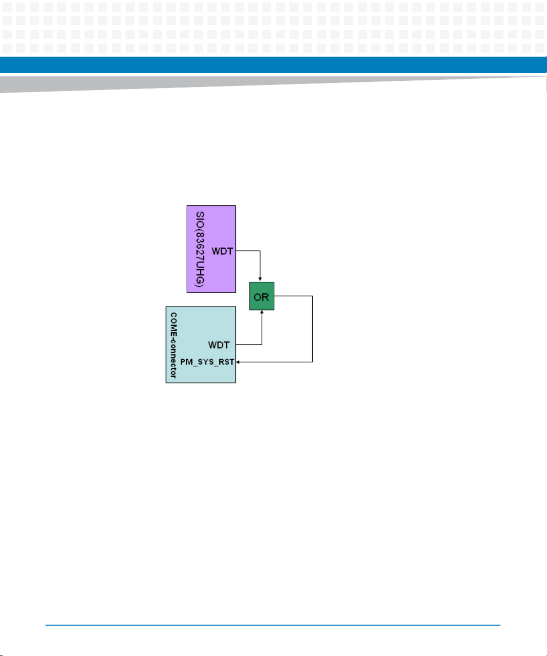
The COMX-CAR-210 provides a watchdog timer (WDT), which is a combination of two
watchdog timers coming from the COM Express connector and Super I/O.
Figure 4-7 Watchdog Timer Block Diagram
A valid WDT output signal resets the COMX-CAR-210. The BIOS disables the boot device
(software is enabled when watchdog application loads). The WDT is disabled before enterting
S3 state, and re-enabled upon exiting S3.
4.12 Real Time Clock (RTC)
There is an onboard battery holder. The battery holder allows for the quick and easy
replacement of a 3 V button cell lithium battery which provides backup power to the onboard
RTC.
64
COMX-CAR-210 Installation and Use (6806800L14D)
Page 65
Appendix A
A Related Documentation
A.1 Artesyn Embedded Technologies - Embedded
Computing Documentation
The publications listed below are referenced in this manual. You can obtain electronic copies of
Artesyn Embedded Technologies - Embedded Computing publications by contacting your
local Artesyn sales office. For released products, you can also visit our Web site for the latest
copies of our product documentation.
1. Go to www.artesyn.com/computing.
2. Under SUPPORT, click TECHNICAL DOCUMENTATION.
3. Under FILTER OPTIONS, click the Document types drop-down list box to select the type of
document you are looking for.
4. In the Search text box, type the product name and click GO.
Table A-1 Artesyn Embedded Technologies - Embedded Computing Publications
Document Title Publication Number
COMX-CAR-210 Quick Start Guide 6806800L15
COMX-CAR-210 Safety Notes Summary 6806800L16
COMX-CAR-210 Installation and Use (6806800L14D)
65
Page 66

Related Documentation
66
COMX-CAR-210 Installation and Use (6806800L14D)
Page 67

Safety Notes
This section provides warnings that precede potentially dangerous procedures throughout
this manual. Instructions contained in the warnings must be followed during all phases of
operation, service, and repair of this equipment. You should also employ all other safety
precautions necessary for the operation of the equipment in your operating environment.
Failure to comply with these precautions or with specific warnings elsewhere in this manual
could result in personal injury or damage to the equipment.
Artesyn Embedded Technologies intends to provide all necessary information to install and
handle the product in this manual. Because of the complexity of this product and its various
uses, we do not guarantee that the given information is complete. If you need additional
information, ask your Artesyn Embedded Technologies representative.
The product has been designed to meet the standard industrial safety requirements. It must
only be used in its specific area of office telecommunication industry, industrial control, and
development. It must not be used in safety critical components, life supporting devices or on
aircraft.
Only personnel trained by Artesyn Embedded Technologies or persons qualified in electronics
or electrical engineering are authorized to install, remove or maintain the product. The
information given in this manual is meant to complete the knowledge of a specialist and must
not be used as replacement for qualified personnel.
Keep away from live circuits inside the equipment. Operating personnel must not remove
equipment covers. Only factory authorized service personnel or other qualified service
personnel is allowed to remove equipment covers for internal subassembly or component
replacement or any internal adjustment.
This product operates with dangerous voltages that can cause injury or death. Use extreme
caution when handling, testing, and adjusting this equipment and its components.
Operation
Product Damage
High humidity and condensation on surfaces cause short circuits.
Do not operate the product outside the specified environmental limits. Make sure the product
is completely dry and there is no moisture on any surface before applying power.
COMX-CAR-210 Installation and Use (6806800L14D)
67
Page 68

Safety Notes
System Overheating
Cooling Vents
Improper cooling can lead to system damage and can void the manufacturer's warranty.
To ensure proper cooling and undisturbed airflow through the system do not obstruct the
ventilation openings of the system. Make sure that the fresh air supply is not mixed with hot
exhaust from other devices.
Installation
Damage of Circuits
Electrostatic discharge and incorrect installation and removal of the product can damage
circuits or shorten their life.
Before touching the product make sure that your are working in an ESD-safe environment or
wear an ESD wrist strap or ESD shoes. Hold the product by its edges and do not touch any
components or circuits.
Damage of the Product and Additional Devices and Modules
Incorrect installation or removal of additional devices or modules damages the product or the
additional devices or modules.
Before installing or removing additional devices or modules, read the respective
documentation and use appropriate tools.
Fans/ Blowers
Pin Damage
Forcing the module into the system may damage connector pins.
If the module hangs during insertion, pull it out and insert it again.
68
COMX-CAR-210 Installation and Use (6806800L14D)
Page 69

Environment
Environmental Damage
Improperly disposing of used products may harm the environment.
Always dispose of used products according to your country’s legislation and manufacturer’s
instructions.
Expansion and FRU Replacement
Personal Injury
During operation, hot surfaces may be present on the heat sinks and components of the
product.
To prevent injury from hot surface do not touch any of the exposed components or heatsinks
on the product when handing. Use the handle and face plate, where applicable, or the board
edge when removing the product from the enclosure.
Safety Notes
COMX-CAR-210 Installation and Use (6806800L14D)
69
Page 70

Safety Notes
70
COMX-CAR-210 Installation and Use (6806800L14D)
Page 71

Sicherheitshinweise
Dieses Kapitel enthält Hinweise, die potentiell gefährlichen Prozeduren innerhalb dieses
Handbuchs vorrangestellt sind. Beachten Sie unbedingt in allen Phasen des Betriebs, der
Wartung und der Reparatur des Systems die Anweisungen, die diesen Hinweisen enthalten
sind. Sie sollten eaußerdem alle anderen Vorsichtsmaßnahmen treffen, die für den Betrieb des
Systems innerhalb Ihrer Betriebsumgebung notwendig sind. Wenn Sie diese
Vorsichtsmaßnahmen oder Sicherheitshinweise, die an anderer Stelle diese Handbuchs
enthalten sind, nicht beachten, kann das Verletzungen oder Schäden am System zur Folge
haben.
Artesyn Embedded Technologies ist darauf bedacht, alle notwendigen Informationen zum
Einbau und zum Umgang mit dem System in diesem Handbuch bereit zu stellen. Da es sich
jedoch bei dem System um ein komplexes Produkt mit vielfältigen Einsatzmöglichkeiten
handelt, können wir die Vollständigkeit der im Handbuch enthaltenen Informationen nicht
garantieren. Falls Sie weitere Informationen benötigen sollten, wenden Sie sich bitte an die für
Sie zuständige Geschäftsstelle von Artesyn Embedded Technologies.
Das Produkt erfüllt die für die Industrie geforderten Sicherheitsvorschriften und darf
ausschließlich für Anwendungen in der Telekommunikationsindustrie, im Zusammenhang mit
Industriesteuerungen und in der Entwicklung verwendet werden. Es darf nicht in
sicherheitskritischen Anwendungen, lebenserhaltenden Geräten oder in Flugzeugen
verwendet werden.
Einbau, Wartung und Betrieb dürfen nur von durch Artesyn Embedded Technologies
ausgebildetem oder im Bereich Elektronik oder Elektrotechnik qualifiziertem Personal
durchgeführt werden. Die in diesem Handbuch enthaltenen Informationen dienen
ausschließlich dazu, das Wissen von Fachpersonal zu ergänzen, können dieses jedoch nicht
ersetzen.
Halten Sie sich von stromführenden Leitungen innerhalb des Systems fern. Entfernen Sie auf
keinen Fall die Systemabdeckung. Nur werksseitig zugelassenes Wartungspersonal oder
anderweitig qualifiziertes Wartungspersonal darf die Systemabdeckung entfernen, um
Systemkomponenten zu ersetzen oder andere Anpassungen vorzunehmen.
Installieren Sie keine Ersatzteile oder führen Sie keine unerlaubten Veränderungen am System
durch, sonst verfällt die Garantie. Wenden Sie sich für Wartung oder Reparatur bitte an die für
Sie zuständige Geschäftsstelle von Artesyn Embedded Technologies. So stellen Sie sicher, dass
alle sicherheitsrelevanten Aspekte beachtet werden.
COMX-CAR-210 Installation and Use (6806800L14D)
71
Page 72

Sicherheitshinweise
Artesyn Embedded Technologies und unsere Zulieferer unternehmen größte Anstrengungen
um sicherzustellen, dass sich Pins und Stecker von Boards vor dem Verlassen der
Produktionsstätte in einwandfreiem Zustand befinden. Verbogene Pins, verursacht durch
fehlerhafte Installation oder durch Installation von Boards mit beschädigten Steckern kann die
durch Artesyn Embedded Technologies gewährte Garantie für Boards und Backplanes
erlöschen lassen.
Dieses Produkt wird mit gefährlichen Spannungen betrieben, die zu Verletzungen und Tod
führen können. Seien Sie im Umgang mit dem Produkt und beim Testen und Anpassen des
Produktes und seiner Komponenten äußerst vorsichtig.
Betrieb
Beschädigung des Systems
Hohe Luftfeuchtigkeit und Kondensat auf den Oberflächen der Produkte kann zu
Kurzschlüssen führen.
Betreiben Sie die Produkte nur innerhalb der angegebenen Grenzwerte für die relative
Luftfeuchtigkeit und Temperatur und stellen Sie vor dem Einschalten des Stroms sicher, dass
sich auf den Produkten kein Kondensat befindet.
System Installation
Beschädigung von Schaltkreisen
Elektrostatische Entladung und unsachgemäßer Ein- und Ausbau des Produktes kann
Schaltkreise beschädigen oder ihre Lebensdauer verkürzen.
Bevor Sie das Produkt oder elektronische Komponenten berühren, vergewissern Sie sich, daß
Sie in einem ESD-geschützten Bereich arbeiten.
Beschädigung des Produktes und der Zusatzmodule
Fehlerhafter Ein- oder Ausbau von Zusatzmodulen führt zu Beschädigung des Produktes oder
der Zusatzmodule.
Lesen Sie deshalb vor dem Ein- oder Ausbau von Zusatzmodulen die Dokumentation und
benutzen Sie angemessenes Werkzeug.
72
COMX-CAR-210 Installation and Use (6806800L14D)
Page 73

Umweltschutz
Umweltverschmutzung
Falsche Entsorgung der Produkte schadet der Umwelt.
Entsorgen Sie alte Produkte gemäß der in Ihrem Land gültigen Gesetzgebung und den
Empfehlungen des Herstellers.
Lüfter
Schäden an Steckern
Wenn Sie das Modul mit Gewalt installieren, können die Anschlussstifte in den Steckern
beschädigt werden.
Falls sich das Modul während der Installation verkantet, ziehen Sie es wieder heraus und führen
Sie sie erneut ein.
Sicherheitshinweise
Erweiterung und FRU Austausch
Verletzungsgefahr
Während des Betriebs können Oberflächen an den Kühlkörpern oder anderen Komponenten
sehr heiß werden.
Um Verletzungen durch Verbrennung zu vermeiden, berühren Sie während der Arbeit keine
Komponenten oder Kühlkörper auf dem Produkt. Fassen Sie das Produkt an den Handles und
der Frontblende an, wenn Sie es aus dem System herausnehmen.
COMX-CAR-210 Installation and Use (6806800L14D)
73
Page 74

Sicherheitshinweise
74
COMX-CAR-210 Installation and Use (6806800L14D)
Page 75

Page 76
Artesyn Embedded Technologies, Artesyn and the Artesyn Embedded Technologies logo are trademarks and service marks of Artesyn Embedded Technologies, Inc.
All other product or service names are the property of their respective owners.
©
2014 Artesyn Embedded Technologies, Inc.
 Loading...