

Page 1

COMX-P40x0 ENP2
Installation and Use
P/N: 6806800R95B
August 2014
Page 2

©
Copyright 2014 Artesyn Embedded Technologies, Inc.
All rights reserved.
Trademarks
Artesyn Embedded Technologies, Artesyn and the Artesyn Embedded Technologies logo are trademarks and service marks of
Artesyn Embedded Technologies, Inc.© 2014 Artesyn Embedded Technologies, Inc. All other product or service names are the
property of their respective owners.
Intel® is a trademark or registered trademark of Intel Corporation or its subsidiaries in the United States and other countries.
Java™ and all other Java-based marks are trademarks or registered trademarks of Oracle America, Inc. in the U.S. and other countries.
Microsoft®, Windows® and Windows Me® are registered trademarks of Microsoft Corporation; and Windows XP™ is a trademark of
Microsoft Corporation.
PICMG®, CompactPCI®, AdvancedTCA™ and the PICMG, CompactPCI and AdvancedTCA logos are registered trademarks of the PCI
Industrial Computer Manufacturers Group.
UNIX® is a registered trademark of The Open Group in the United States and other countries.
Notice
While reasonable efforts have been made to assure the accuracy of this document, Artesyn assumes no liability resulting from any
omissions in this document, or from the use of the information obtained therein. Artesyn reserves the right to revise this document
and to make changes from time to time in the content hereof without obligation of Artesyn to notify any person of such revision or
changes.
Electronic versions of this material may be read online, downloaded for personal use, or referenced in another document as a URL to
an Artesyn website. The text itself may not be published commercially in print or electronic form, edited, translated, or otherwise
altered without the permission of Artesyn.
It is possible that this publication may contain reference to or information about Artesyn products (machines and programs),
programming, or services that are not available in your country. Such references or information must not be construed to mean that
Artesyn intends to announce such Artesyn products, programming, or services in your country.
Limited and Restricted Rights Legend
If the documentation contained herein is supplied, directly or indirectly, to the U.S. Government, the following notice shall apply
unless otherwise agreed to in writing by Artesyn.
Use, duplication, or disclosure by the Government is subject to restrictions as set forth in subparagraph (b)(3) of the Rights in
Technical Data clause at DFARS 252.227-7013 (Nov. 1995) and of the Rights in Noncommercial Computer Software and
Documentation clause at DFARS 252.227-7014 (Jun. 1995).
Contact Address
Artesyn Embedded Technologies Artesyn Embedded Technologies
Marketing Communications
2900 S. Diablo Way, Suite 190
Tempe, Arizona 85282
Lilienthalstr. 17-19
85579 Neubiberg/Munich
Germany
Page 3

Contents
Contents
About this Manual . . . . . . . . . . . . . . . . . . . . . . . . . . . . . . . . . . . . . . . . . . . . . . . . . . . . . . . . . . . . . . . . . . . . . . . 11
1 Introduction . . . . . . . . . . . . . . . . . . . . . . . . . . . . . . . . . . . . . . . . . . . . . . . . . . . . . . . . . . . . . . . . . . . . . . . . . 15
1.1 Overview . . . . . . . . . . . . . . . . . . . . . . . . . . . . . . . . . . . . . . . . . . . . . . . . . . . . . . . . . . . . . . . . . . . . . . . . . . 15
1.2 Standard Compliances . . . . . . . . . . . . . . . . . . . . . . . . . . . . . . . . . . . . . . . . . . . . . . . . . . . . . . . . . . . . . . 16
1.3 Mechanical Data . . . . . . . . . . . . . . . . . . . . . . . . . . . . . . . . . . . . . . . . . . . . . . . . . . . . . . . . . . . . . . . . . . . 19
1.3.1 COMX-P4080 ENP2. . . . . . . . . . . . . . . . . . . . . . . . . . . . . . . . . . . . . . . . . . . . . . . . . . . . . . . . . . . 21
1.3.2 COMX-P4040 ENP2. . . . . . . . . . . . . . . . . . . . . . . . . . . . . . . . . . . . . . . . . . . . . . . . . . . . . . . . . . . 23
1.4 Ordering Information . . . . . . . . . . . . . . . . . . . . . . . . . . . . . . . . . . . . . . . . . . . . . . . . . . . . . . . . . . . . . . . 24
1.5 Product Identification . . . . . . . . . . . . . . . . . . . . . . . . . . . . . . . . . . . . . . . . . . . . . . . . . . . . . . . . . . . . . . . 24
1.5.1 COMX-P4080 ENP2. . . . . . . . . . . . . . . . . . . . . . . . . . . . . . . . . . . . . . . . . . . . . . . . . . . . . . . . . . . 25
1.5.2 COMX-P4040 ENP2. . . . . . . . . . . . . . . . . . . . . . . . . . . . . . . . . . . . . . . . . . . . . . . . . . . . . . . . . . . 25
2 Hardware Preparation and Installation . . . . . . . . . . . . . . . . . . . . . . . . . . . . . . . . . . . . . . . . . . . . . . . . . 27
2.1 Environmental and Power Requirements . . . . . . . . . . . . . . . . . . . . . . . . . . . . . . . . . . . . . . . . . . . . . . 27
2.1.1 Environmental Requirements. . . . . . . . . . . . . . . . . . . . . . . . . . . . . . . . . . . . . . . . . . . . . . . . . . 27
2.2 Unpacking and Inspecting the Enclosure . . . . . . . . . . . . . . . . . . . . . . . . . . . . . . . . . . . . . . . . . . . . . . 29
2.3 Installing and Removing the Module on the Carrier Board . . . . . . . . . . . . . . . . . . . . . . . . . . . . . . . 30
3 Controls, LEDs, and Connectors . . . . . . . . . . . . . . . . . . . . . . . . . . . . . . . . . . . . . . . . . . . . . . . . . . . . . . . . 35
3.1 Connectors and Switches . . . . . . . . . . . . . . . . . . . . . . . . . . . . . . . . . . . . . . . . . . . . . . . . . . . . . . . . . . . . 35
3.1.1 On-Board Connectors . . . . . . . . . . . . . . . . . . . . . . . . . . . . . . . . . . . . . . . . . . . . . . . . . . . . . . . . 35
3.1.2 ON-BOARD LEDS . . . . . . . . . . . . . . . . . . . . . . . . . . . . . . . . . . . . . . . . . . . . . . . . . . . . . . . . . . . . . 37
3.1.3 COMX AB-CD Connectors . . . . . . . . . . . . . . . . . . . . . . . . . . . . . . . . . . . . . . . . . . . . . . . . . . . . . 37
4 Functional Description . . . . . . . . . . . . . . . . . . . . . . . . . . . . . . . . . . . . . . . . . . . . . . . . . . . . . . . . . . . . . . . . 57
4.1 Overview . . . . . . . . . . . . . . . . . . . . . . . . . . . . . . . . . . . . . . . . . . . . . . . . . . . . . . . . . . . . . . . . . . . . . . . . . . 57
4.2 Block Diagram . . . . . . . . . . . . . . . . . . . . . . . . . . . . . . . . . . . . . . . . . . . . . . . . . . . . . . . . . . . . . . . . . . . . . 58
4.3 Processor Core and Cache Memory Complex . . . . . . . . . . . . . . . . . . . . . . . . . . . . . . . . . . . . . . . . . . . 59
4.4 Integrated Memory Controller . . . . . . . . . . . . . . . . . . . . . . . . . . . . . . . . . . . . . . . . . . . . . . . . . . . . . . . 59
4.5 Local Bus . . . . . . . . . . . . . . . . . . . . . . . . . . . . . . . . . . . . . . . . . . . . . . . . . . . . . . . . . . . . . . . . . . . . . . . . . . 60
4.5.1 Clock . . . . . . . . . . . . . . . . . . . . . . . . . . . . . . . . . . . . . . . . . . . . . . . . . . . . . . . . . . . . . . . . . . . . . . . 61
4.5.2 NOR FLASH. . . . . . . . . . . . . . . . . . . . . . . . . . . . . . . . . . . . . . . . . . . . . . . . . . . . . . . . . . . . . . . . . . 61
COMX-P40x0 ENP2 Installation and Use (6806800R95B)
3
Page 4

Contents
Contents
Contents
4.5.3 NAND FLASH . . . . . . . . . . . . . . . . . . . . . . . . . . . . . . . . . . . . . . . . . . . . . . . . . . . . . . . . . . . . . . . . 62
4.6 SERDES Block . . . . . . . . . . . . . . . . . . . . . . . . . . . . . . . . . . . . . . . . . . . . . . . . . . . . . . . . . . . . . . . . . . . . . . 62
4.7 Thermal Management . . . . . . . . . . . . . . . . . . . . . . . . . . . . . . . . . . . . . . . . . . . . . . . . . . . . . . . . . . . . . . 65
4.8 Main Memory . . . . . . . . . . . . . . . . . . . . . . . . . . . . . . . . . . . . . . . . . . . . . . . . . . . . . . . . . . . . . . . . . . . . . . 66
4.8.1 Memory Interface . . . . . . . . . . . . . . . . . . . . . . . . . . . . . . . . . . . . . . . . . . . . . . . . . . . . . . . . . . . . 66
4.8.2 Memory Map . . . . . . . . . . . . . . . . . . . . . . . . . . . . . . . . . . . . . . . . . . . . . . . . . . . . . . . . . . . . . . . . 67
4.9 GPIO . . . . . . . . . . . . . . . . . . . . . . . . . . . . . . . . . . . . . . . . . . . . . . . . . . . . . . . . . . . . . . . . . . . . . . . . . . . . . . 68
4.10 SDHC . . . . . . . . . . . . . . . . . . . . . . . . . . . . . . . . . . . . . . . . . . . . . . . . . . . . . . . . . . . . . . . . . . . . . . . . . . . . . 70
4.11 SPI Interface . . . . . . . . . . . . . . . . . . . . . . . . . . . . . . . . . . . . . . . . . . . . . . . . . . . . . . . . . . . . . . . . . . . . . . . 70
4.12 LAN . . . . . . . . . . . . . . . . . . . . . . . . . . . . . . . . . . . . . . . . . . . . . . . . . . . . . . . . . . . . . . . . . . . . . . . . . . . . . . . 71
4.12.1 MDIO . . . . . . . . . . . . . . . . . . . . . . . . . . . . . . . . . . . . . . . . . . . . . . . . . . . . . . . . . . . . . . . . . . . . . . . 71
4.13 PHY . . . . . . . . . . . . . . . . . . . . . . . . . . . . . . . . . . . . . . . . . . . . . . . . . . . . . . . . . . . . . . . . . . . . . . . . . . . . . . . 73
4.14 UART Interface . . . . . . . . . . . . . . . . . . . . . . . . . . . . . . . . . . . . . . . . . . . . . . . . . . . . . . . . . . . . . . . . . . . . . 73
4.15 Real Time Clock . . . . . . . . . . . . . . . . . . . . . . . . . . . . . . . . . . . . . . . . . . . . . . . . . . . . . . . . . . . . . . . . . . . . 73
4.16 Watchdog Timer . . . . . . . . . . . . . . . . . . . . . . . . . . . . . . . . . . . . . . . . . . . . . . . . . . . . . . . . . . . . . . . . . . . 73
4.17 USB . . . . . . . . . . . . . . . . . . . . . . . . . . . . . . . . . . . . . . . . . . . . . . . . . . . . . . . . . . . . . . . . . . . . . . . . . . . . . . . 73
4.18 I2C Interface . . . . . . . . . . . . . . . . . . . . . . . . . . . . . . . . . . . . . . . . . . . . . . . . . . . . . . . . . . . . . . . . . . . . . . . 74
4.18.1 I2C Device Thermal Sensor . . . . . . . . . . . . . . . . . . . . . . . . . . . . . . . . . . . . . . . . . . . . . . . . . . . . 76
4.18.2 I2C Device EEPROM . . . . . . . . . . . . . . . . . . . . . . . . . . . . . . . . . . . . . . . . . . . . . . . . . . . . . . . . . . 76
4.18.3 I2C Device WDT. . . . . . . . . . . . . . . . . . . . . . . . . . . . . . . . . . . . . . . . . . . . . . . . . . . . . . . . . . . . . . 76
4.18.4 I2C Device RTC . . . . . . . . . . . . . . . . . . . . . . . . . . . . . . . . . . . . . . . . . . . . . . . . . . . . . . . . . . . . . . 77
4.18.5 I2C Device Clock Generators. . . . . . . . . . . . . . . . . . . . . . . . . . . . . . . . . . . . . . . . . . . . . . . . . . . 77
5 Clock Structure. . . . . . . . . . . . . . . . . . . . . . . . . . . . . . . . . . . . . . . . . . . . . . . . . . . . . . . . . . . . . . . . . . . . . . . 79
5.1 Overview . . . . . . . . . . . . . . . . . . . . . . . . . . . . . . . . . . . . . . . . . . . . . . . . . . . . . . . . . . . . . . . . . . . . . . . . . . 79
6 Power Domains . . . . . . . . . . . . . . . . . . . . . . . . . . . . . . . . . . . . . . . . . . . . . . . . . . . . . . . . . . . . . . . . . . . . . . 81
6.1 Overview . . . . . . . . . . . . . . . . . . . . . . . . . . . . . . . . . . . . . . . . . . . . . . . . . . . . . . . . . . . . . . . . . . . . . . . . . . 81
6.2 Power Controlling Sequence . . . . . . . . . . . . . . . . . . . . . . . . . . . . . . . . . . . . . . . . . . . . . . . . . . . . . . . . . 82
7 BSP . . . . . . . . . . . . . . . . . . . . . . . . . . . . . . . . . . . . . . . . . . . . . . . . . . . . . . . . . . . . . . . . . . . . . . . . . . . . . . . . . 83
7.1 Overview . . . . . . . . . . . . . . . . . . . . . . . . . . . . . . . . . . . . . . . . . . . . . . . . . . . . . . . . . . . . . . . . . . . . . . . . . . 83
7.2 Setup Requirements . . . . . . . . . . . . . . . . . . . . . . . . . . . . . . . . . . . . . . . . . . . . . . . . . . . . . . . . . . . . . . . . 83
4
COMX-P40x0 ENP2 Installation and Use (6806800R95B)
Page 5

Contents
7.3 Basic Commands . . . . . . . . . . . . . . . . . . . . . . . . . . . . . . . . . . . . . . . . . . . . . . . . . . . . . . . . . . . . . . . . . . . 83
7.4 BSP Build Requirements . . . . . . . . . . . . . . . . . . . . . . . . . . . . . . . . . . . . . . . . . . . . . . . . . . . . . . . . . . . . . 84
7.4.1 Install Build Tools of SDK1.0 . . . . . . . . . . . . . . . . . . . . . . . . . . . . . . . . . . . . . . . . . . . . . . . . . . . 85
7.5 BSP Source Code Package . . . . . . . . . . . . . . . . . . . . . . . . . . . . . . . . . . . . . . . . . . . . . . . . . . . . . . . . . . . 86
7.5.1 De-Compose Source Code Package . . . . . . . . . . . . . . . . . . . . . . . . . . . . . . . . . . . . . . . . . . . . 86
7.6 Basic Environment Variable Settings . . . . . . . . . . . . . . . . . . . . . . . . . . . . . . . . . . . . . . . . . . . . . . . . . . 87
7.6.1 Setup Build Environment. . . . . . . . . . . . . . . . . . . . . . . . . . . . . . . . . . . . . . . . . . . . . . . . . . . . . . 87
7.6.2 Network Variables. . . . . . . . . . . . . . . . . . . . . . . . . . . . . . . . . . . . . . . . . . . . . . . . . . . . . . . . . . . . 87
7.6.3 Filename Variables for BSP Components . . . . . . . . . . . . . . . . . . . . . . . . . . . . . . . . . . . . . . . . 88
7.6.4 Address Variables for BSP Components on NOR Flash. . . . . . . . . . . . . . . . . . . . . . . . . . . . . 88
7.6.5 Address Variables for the Boot Components in RAM . . . . . . . . . . . . . . . . . . . . . . . . . . . . . . 89
7.6.6 Device Variables . . . . . . . . . . . . . . . . . . . . . . . . . . . . . . . . . . . . . . . . . . . . . . . . . . . . . . . . . . . . . 89
7.6.7 HWCONFIG Variable. . . . . . . . . . . . . . . . . . . . . . . . . . . . . . . . . . . . . . . . . . . . . . . . . . . . . . . . . . 89
7.6.8 Bootargs Variable . . . . . . . . . . . . . . . . . . . . . . . . . . . . . . . . . . . . . . . . . . . . . . . . . . . . . . . . . . . . 90
7.6.9 Bootup Variables. . . . . . . . . . . . . . . . . . . . . . . . . . . . . . . . . . . . . . . . . . . . . . . . . . . . . . . . . . . . . 90
7.7 Checking the BSP Version . . . . . . . . . . . . . . . . . . . . . . . . . . . . . . . . . . . . . . . . . . . . . . . . . . . . . . . . . . . 91
7.8 CPU . . . . . . . . . . . . . . . . . . . . . . . . . . . . . . . . . . . . . . . . . . . . . . . . . . . . . . . . . . . . . . . . . . . . . . . . . . . . . . . 93
7.9 Address Space . . . . . . . . . . . . . . . . . . . . . . . . . . . . . . . . . . . . . . . . . . . . . . . . . . . . . . . . . . . . . . . . . . . . . 93
7.10 DDR3 SDRAM . . . . . . . . . . . . . . . . . . . . . . . . . . . . . . . . . . . . . . . . . . . . . . . . . . . . . . . . . . . . . . . . . . . . . . 95
7.11 GPIO . . . . . . . . . . . . . . . . . . . . . . . . . . . . . . . . . . . . . . . . . . . . . . . . . . . . . . . . . . . . . . . . . . . . . . . . . . . . . . 96
7.12 UART . . . . . . . . . . . . . . . . . . . . . . . . . . . . . . . . . . . . . . . . . . . . . . . . . . . . . . . . . . . . . . . . . . . . . . . . . . . . . 97
7.13 NOR Flash . . . . . . . . . . . . . . . . . . . . . . . . . . . . . . . . . . . . . . . . . . . . . . . . . . . . . . . . . . . . . . . . . . . . . . . . . 98
7.14 NAND Flash . . . . . . . . . . . . . . . . . . . . . . . . . . . . . . . . . . . . . . . . . . . . . . . . . . . . . . . . . . . . . . . . . . . . . . . . 99
7.15 I2C . . . . . . . . . . . . . . . . . . . . . . . . . . . . . . . . . . . . . . . . . . . . . . . . . . . . . . . . . . . . . . . . . . . . . . . . . . . . . . 100
7.15.1 ID EEPROM . . . . . . . . . . . . . . . . . . . . . . . . . . . . . . . . . . . . . . . . . . . . . . . . . . . . . . . . . . . . . . . . . 101
7.15.2 Board EEPROM. . . . . . . . . . . . . . . . . . . . . . . . . . . . . . . . . . . . . . . . . . . . . . . . . . . . . . . . . . . . . . 102
7.15.3 Real Time Clock (RTC) and Watchdog Timer (WDT) . . . . . . . . . . . . . . . . . . . . . . . . . . . . . 103
7.15.4 DTT . . . . . . . . . . . . . . . . . . . . . . . . . . . . . . . . . . . . . . . . . . . . . . . . . . . . . . . . . . . . . . . . . . . . . . . 105
7.16 SPI . . . . . . . . . . . . . . . . . . . . . . . . . . . . . . . . . . . . . . . . . . . . . . . . . . . . . . . . . . . . . . . . . . . . . . . . . . . . . . . 105
7.17 MMC/SDHC . . . . . . . . . . . . . . . . . . . . . . . . . . . . . . . . . . . . . . . . . . . . . . . . . . . . . . . . . . . . . . . . . . . . . . . 106
7.18 USB . . . . . . . . . . . . . . . . . . . . . . . . . . . . . . . . . . . . . . . . . . . . . . . . . . . . . . . . . . . . . . . . . . . . . . . . . . . . . .106
7.19 SerDes . . . . . . . . . . . . . . . . . . . . . . . . . . . . . . . . . . . . . . . . . . . . . . . . . . . . . . . . . . . . . . . . . . . . . . . . . . . 107
7.20 Network . . . . . . . . . . . . . . . . . . . . . . . . . . . . . . . . . . . . . . . . . . . . . . . . . . . . . . . . . . . . . . . . . . . . . . . . . . 110
7.21 Build BSP Images . . . . . . . . . . . . . . . . . . . . . . . . . . . . . . . . . . . . . . . . . . . . . . . . . . . . . . . . . . . . . . . . . . 114
7.21.1 Build U-Boot. . . . . . . . . . . . . . . . . . . . . . . . . . . . . . . . . . . . . . . . . . . . . . . . . . . . . . . . . . . . . . . . 115
7.21.2 Build Linux Kernel . . . . . . . . . . . . . . . . . . . . . . . . . . . . . . . . . . . . . . . . . . . . . . . . . . . . . . . . . . . 115
COMX-P40x0 ENP2 Installation and Use (6806800R95B)
5
Page 6

Contents
Contents
Contents
7.21.3 Build ROOTFS. . . . . . . . . . . . . . . . . . . . . . . . . . . . . . . . . . . . . . . . . . . . . . . . . . . . . . . . . . . . . . . 116
7.21.4 Build Misc Firmware . . . . . . . . . . . . . . . . . . . . . . . . . . . . . . . . . . . . . . . . . . . . . . . . . . . . . . . . . 117
7.22 Deploy BSP Images . . . . . . . . . . . . . . . . . . . . . . . . . . . . . . . . . . . . . . . . . . . . . . . . . . . . . . . . . . . . . . . .117
7.22.1 Pre-Deployment Steps. . . . . . . . . . . . . . . . . . . . . . . . . . . . . . . . . . . . . . . . . . . . . . . . . . . . . . . 117
7.22.2 Deploying BSP Images on NOR FLASH . . . . . . . . . . . . . . . . . . . . . . . . . . . . . . . . . . . . . . . . . 119
7.23 Boot . . . . . . . . . . . . . . . . . . . . . . . . . . . . . . . . . . . . . . . . . . . . . . . . . . . . . . . . . . . . . . . . . . . . . . . . . . . . . 119
7.23.1 RAMboot . . . . . . . . . . . . . . . . . . . . . . . . . . . . . . . . . . . . . . . . . . . . . . . . . . . . . . . . . . . . . . . . . . 120
7.23.2 NORboot. . . . . . . . . . . . . . . . . . . . . . . . . . . . . . . . . . . . . . . . . . . . . . . . . . . . . . . . . . . . . . . . . . . 120
7.23.3 NANDboot . . . . . . . . . . . . . . . . . . . . . . . . . . . . . . . . . . . . . . . . . . . . . . . . . . . . . . . . . . . . . . . . . 121
7.23.4 NFSboot . . . . . . . . . . . . . . . . . . . . . . . . . . . . . . . . . . . . . . . . . . . . . . . . . . . . . . . . . . . . . . . . . . .122
7.23.5 USBFATboot and USBEXT2boot . . . . . . . . . . . . . . . . . . . . . . . . . . . . . . . . . . . . . . . . . . . . . . .122
7.23.6 MMCFATboot and MMCEXT2boot. . . . . . . . . . . . . . . . . . . . . . . . . . . . . . . . . . . . . . . . . . . . . 123
A Related Documentation . . . . . . . . . . . . . . . . . . . . . . . . . . . . . . . . . . . . . . . . . . . . . . . . . . . . . . . . . . . . . .125
A.1 Artesyn Embedded Technologies - Embedded Computing Documentation . . . . . . . . . . . . . . . 125
Safety Notes . . . . . . . . . . . . . . . . . . . . . . . . . . . . . . . . . . . . . . . . . . . . . . . . . . . . . . . . . . . . . . . . . . . . . . . . . . . .127
6
COMX-P40x0 ENP2 Installation and Use (6806800R95B)
Page 7

List of Tables
Table 1-1 Standard Compliances . . . . . . . . . . . . . . . . . . . . . . . . . . . . . . . . . . . . . . . . . . . . . . . . . . . . . . . . . . 16
Table 1-2 COMX-P4080 ENP2 PCB Dimensions . . . . . . . . . . . . . . . . . . . . . . . . . . . . . . . . . . . . . . . . . . . . . 22
Table 1-3 COMX-P4040 ENP2 PCB Dimensions . . . . . . . . . . . . . . . . . . . . . . . . . . . . . . . . . . . . . . . . . . . . . 24
Table 1-4 Ordering Information . . . . . . . . . . . . . . . . . . . . . . . . . . . . . . . . . . . . . . . . . . . . . . . . . . . . . . . . . . . 24
Table 2-1 Environmental Requirements . . . . . . . . . . . . . . . . . . . . . . . . . . . . . . . . . . . . . . . . . . . . . . . . . . . . 27
Table 2-2 Critical Temperature Spots . . . . . . . . . . . . . . . . . . . . . . . . . . . . . . . . . . . . . . . . . . . . . . . . . . . . . . 28
Table 2-3 Current Drawn . . . . . . . . . . . . . . . . . . . . . . . . . . . . . . . . . . . . . . . . . . . . . . . . . . . . . . . . . . . . . . . . . 29
Table 2-4 COMX-P4080-4G-E-ENP2 . . . . . . . . . . . . . . . . . . . . . . . . . . . . . . . . . . . . . . . . . . . . . . . . . . . . . . . 29
Table 3-1 P4080 COP Header Pin-out . . . . . . . . . . . . . . . . . . . . . . . . . . . . . . . . . . . . . . . . . . . . . . . . . . . . . . 35
Table 3-2 P4040 COP Header Pin-out . . . . . . . . . . . . . . . . . . . . . . . . . . . . . . . . . . . . . . . . . . . . . . . . . . . . . . 36
Table 3-3 Module LED Status . . . . . . . . . . . . . . . . . . . . . . . . . . . . . . . . . . . . . . . . . . . . . . . . . . . . . . . . . . . . . 37
Table 3-4 COMX AB-CD Connectors . . . . . . . . . . . . . . . . . . . . . . . . . . . . . . . . . . . . . . . . . . . . . . . . . . . . . . . 37
Table 4-1 NOR FLASH Map . . . . . . . . . . . . . . . . . . . . . . . . . . . . . . . . . . . . . . . . . . . . . . . . . . . . . . . . . . . . . . . 61
Table 4-2 NAND FLASH Map . . . . . . . . . . . . . . . . . . . . . . . . . . . . . . . . . . . . . . . . . . . . . . . . . . . . . . . . . . . . . . 62
Table 4-3 Options of the SERDES routed to COM Express Connectors . . . . . . . . . . . . . . . . . . . . . . . . . . 63
Table 4-4 Memory Map . . . . . . . . . . . . . . . . . . . . . . . . . . . . . . . . . . . . . . . . . . . . . . . . . . . . . . . . . . . . . . . . . . 67
Table 4-5 GPIO . . . . . . . . . . . . . . . . . . . . . . . . . . . . . . . . . . . . . . . . . . . . . . . . . . . . . . . . . . . . . . . . . . . . . . . . . 68
Table 4-6 GPIO . . . . . . . . . . . . . . . . . . . . . . . . . . . . . . . . . . . . . . . . . . . . . . . . . . . . . . . . . . . . . . . . . . . . . . . . . 70
Table 4-7 SD or Micro SD card on the Carrier . . . . . . . . . . . . . . . . . . . . . . . . . . . . . . . . . . . . . . . . . . . . . . . 70
Table 4-8 I2C Interface . . . . . . . . . . . . . . . . . . . . . . . . . . . . . . . . . . . . . . . . . . . . . . . . . . . . . . . . . . . . . . . . . . 75
Table 5-1 Configuration of the frequency of SERDES reference clock by carrier . . . . . . . . . . . . . . . . . . 79
Table 5-2 Configuration of the frequency of SERDES reference clock by GPIO . . . . . . . . . . . . . . . . . . . 80
Table 7-1 Basic U-Boot Commands . . . . . . . . . . . . . . . . . . . . . . . . . . . . . . . . . . . . . . . . . . . . . . . . . . . . . . . . 83
Table 7-2 BSP Source Code Package Layout . . . . . . . . . . . . . . . . . . . . . . . . . . . . . . . . . . . . . . . . . . . . . . . . 86
Table 7-3 COMX-P4080 Address Space . . . . . . . . . . . . . . . . . . . . . . . . . . . . . . . . . . . . . . . . . . . . . . . . . . . . 94
Table 7-4 GPIO States . . . . . . . . . . . . . . . . . . . . . . . . . . . . . . . . . . . . . . . . . . . . . . . . . . . . . . . . . . . . . . . . . . . 96
Table 7-5 GPIO Command Usage . . . . . . . . . . . . . . . . . . . . . . . . . . . . . . . . . . . . . . . . . . . . . . . . . . . . . . . . . 97
Table 7-6 NOR Flash Command Usage . . . . . . . . . . . . . . . . . . . . . . . . . . . . . . . . . . . . . . . . . . . . . . . . . . . . . 98
Table 7-7 NAND Flash Command Usage . . . . . . . . . . . . . . . . . . . . . . . . . . . . . . . . . . . . . . . . . . . . . . . . . . . 99
Table 7-8 U-Boot I2C Utilities . . . . . . . . . . . . . . . . . . . . . . . . . . . . . . . . . . . . . . . . . . . . . . . . . . . . . . . . . . . .100
Table 7-9 Network Ports Naming Rules in U-Boot . . . . . . . . . . . . . . . . . . . . . . . . . . . . . . . . . . . . . . . . . . 110
Table 7-10 Valid Network Ports Combination of SerDes/RCW . . . . . . . . . . . . . . . . . . . . . . . . . . . . . . . . . 111
Table 7-11 UDEV Rules for Network Ports in Linux . . . . . . . . . . . . . . . . . . . . . . . . . . . . . . . . . . . . . . . . . . .113
Table A-1 Artesyn Embedded Technologies - Embedded Computing Publications . . . . . . . . . . . . . . 125
COMX-P40x0 ENP2 Installation and Use (6806800R95B)
7
Page 8

List of Tables
8
COMX-P40x0 ENP2 Installation and Use (6806800R95B)
Page 9

List of Figures
Figure 1-1 Declaration of Conformity . . . . . . . . . . . . . . . . . . . . . . . . . . . . . . . . . . . . . . . . . . . . . . . . 18
Figure 1-2 COMX-P40X0-ENP2 Top View . . . . . . . . . . . . . . . . . . . . . . . . . . . . . . . . . . . . . . . . . . . . . 19
Figure 1-3 COMX-P40X0-ENP2 Bottom View . . . . . . . . . . . . . . . . . . . . . . . . . . . . . . . . . . . . . . . . . 20
Figure 1-4 COMX-P4080 ENP2 Mechanical Dimensions (Top and side views) . . . . . . . . . . . . . 21
Figure 1-5 COMX-P4040 ENP2 Mechanical Dimensions (Top and side views) . . . . . . . . . . . . . 23
Figure 1-6 COMX-P4080 ENP2 Serial Number Location . . . . . . . . . . . . . . . . . . . . . . . . . . . . . . . . 25
Figure 1-7 COMX-P4040 ENP2 Serial Number Location . . . . . . . . . . . . . . . . . . . . . . . . . . . . . . . . 25
Figure 2-1 Mounting Module on Carrier Board . . . . . . . . . . . . . . . . . . . . . . . . . . . . . . . . . . . . . . . . 32
Figure 2-2 Heat-sink installation . . . . . . . . . . . . . . . . . . . . . . . . . . . . . . . . . . . . . . . . . . . . . . . . . . . . 33
Figure 4-1 COMX-P40x0 ENP2 Block Diagram . . . . . . . . . . . . . . . . . . . . . . . . . . . . . . . . . . . . . . . . 58
Figure 4-2 Distribution of Local Bus on P40x0 . . . . . . . . . . . . . . . . . . . . . . . . . . . . . . . . . . . . . . . . 60
Figure 4-3 Distribution of SERDES Lanes . . . . . . . . . . . . . . . . . . . . . . . . . . . . . . . . . . . . . . . . . . . . . 64
Figure 4-4 Module Thermal Management . . . . . . . . . . . . . . . . . . . . . . . . . . . . . . . . . . . . . . . . . . . . 65
Figure 4-5 Memory Interface . . . . . . . . . . . . . . . . . . . . . . . . . . . . . . . . . . . . . . . . . . . . . . . . . . . . . . . 66
Figure 4-6 Distribution of GPIO . . . . . . . . . . . . . . . . . . . . . . . . . . . . . . . . . . . . . . . . . . . . . . . . . . . . . 69
Figure 4-7 MDIO Routing . . . . . . . . . . . . . . . . . . . . . . . . . . . . . . . . . . . . . . . . . . . . . . . . . . . . . . . . . . 72
Figure 4-8 Distribution of I2C buses . . . . . . . . . . . . . . . . . . . . . . . . . . . . . . . . . . . . . . . . . . . . . . . . . 75
Figure 5-1 Clock Distribution . . . . . . . . . . . . . . . . . . . . . . . . . . . . . . . . . . . . . . . . . . . . . . . . . . . . . . . 79
Figure 6-1 Power Tree . . . . . . . . . . . . . . . . . . . . . . . . . . . . . . . . . . . . . . . . . . . . . . . . . . . . . . . . . . . . . 81
Figure 6-2 Power Sequence of COMX-P40x0 ENP2 . . . . . . . . . . . . . . . . . . . . . . . . . . . . . . . . . . . . 82
Figure 7-1 COMX-P4080 CPU Information . . . . . . . . . . . . . . . . . . . . . . . . . . . . . . . . . . . . . . . . . . . 93
Figure 7-2 Example of Boot Up Message in U-Boot . . . . . . . . . . . . . . . . . . . . . . . . . . . . . . . . . . . 109
COMX-P40x0 ENP2 Installation and Use (6806800R95B)
9
Page 10

List of Figures
10
COMX-P40x0 ENP2 Installation and Use (6806800R95B)
Page 11
About this Manual
Overview of Contents
This manual is divided into the following chapters and appendices.
Introduction provides an overview of the module's features.
Hardware Preparation and Installation provides instructions for installing and removing the
module.
Controls, LEDs, and Connectors provides pin assignments for the various connectors on the
module.
Functional Description describes the functions of the various components on the module.
Clock Structure describes the clock distribution and the setup utility used to configure the
module.
Power Domains describes the power supply system for the module.
BSP describes how to build the Basic Support Package (BSP) and deploy the built images on
the module.
Related Documentation provides a list of related product documentation, manufacturer’s
documents, and industry standard specifications.
Safety Notes summarizes the safety instructions in the manual.
Abbreviations
This document uses the following abbreviations:
TERM MEANING
AAmps
ACPI Advanced Configuration Power Interface - software standard to
implement power saving modes in PC-AT systems
EEPROM Electrically Erasable Programmable Read-Only Memory
GPI General Purpose Input
GPIO General Purpose Input Output
GPO General Purpose Output
COMX-P40x0 ENP2 Installation and Use (6806800R95B)
11
Page 12

About this Manual
TERM MEANING
I2C Inter Integrated Circuit - 2 wire (clock and data) signaling scheme
IDE Integrated Device Electronics - parallel interface for hard disk drives -
LPC Low Pin-Count Interface: a low speed interface used for peripheral
LVDS Low Voltage Differential Signaling - widely used as a physical
PCI Peripheral Component Interface
PCI-E Peripheral Component Interface Express - next-generation high
About this Manual
allowing communication between integrated circuits, primarily used
to read and load registers values.
also known as PATA
circuits such as Super I/O controllers, which typically combine
legacy-device support into a single IC.
interface for TFT flat panels. LVDS can be used for many high-speed
signaling applications. In this document, it refers only to TFT flatpanel applications.
speed Serialized I/O bus
PHY Ethernet controller physical layer device
Pin-out Type A reference to one of five COM ExpressTM definitions for what signals
appear on the COM ExpressTM module connector pins.
SPD Serial Presence Detect - refers to serial EEPROM on DRAMs that has
DRAM module configuration information
S0, S1, S2, S3, S4, S5 System states describing the power and activity level
S0 Full power, all devices powered S1 S2
S3 Suspend to RAM System context stored in RAM; RAM is in standby
S4 Suspend to Disk System context stored on disk
S5 Soft Off Main power rail off, only standby power rail present
SATA Serial AT Attachment: serial-interface standard for hard disks
SBC Single Board Computer
Super I/O An integrated circuit typically interfaced via the LPC bus that
provides legacy PC I/O functions including PS2 keyboard and mouse
ports, serial and parallel port(s) and a floppy interface.
USB Universal Serial Bus
VGA Video Graphics Adapter
WDT Watch Dog Timer.
12
COMX-P40x0 ENP2 Installation and Use (6806800R95B)
Page 13

Conventions
The following table describes the conventions used throughout this manual.
Notation Description
0x00000000 Typical notation for hexadecimal numbers (digits are
0b0000 Same for binary numbers (digits are 0 and 1)
bold Used to emphasize a word
Screen Used for on-screen output and code related elements
Courier + Bold Used to characterize user input and to separate it
Reference Used for references and for table and figure
About this Manual
0 through F), for example used for addresses and
offsets
or commands in body text
from system output
descriptions
File > Exit Notation for selecting a submenu
<text> Notation for variables and keys
[text] Notation for software buttons to click on the screen
... Repeated item for example node 1, node 2, ..., node
.
.
.
.. Ranges, for example: 0..4 means one of the integers
| Logical OR
COMX-P40x0 ENP2 Installation and Use (6806800R95B)
and parameter description
12
Omission of information from example/command
that is not necessary at the time being
0,1,2,3, and 4 (used in registers)
13
Page 14
About this Manual
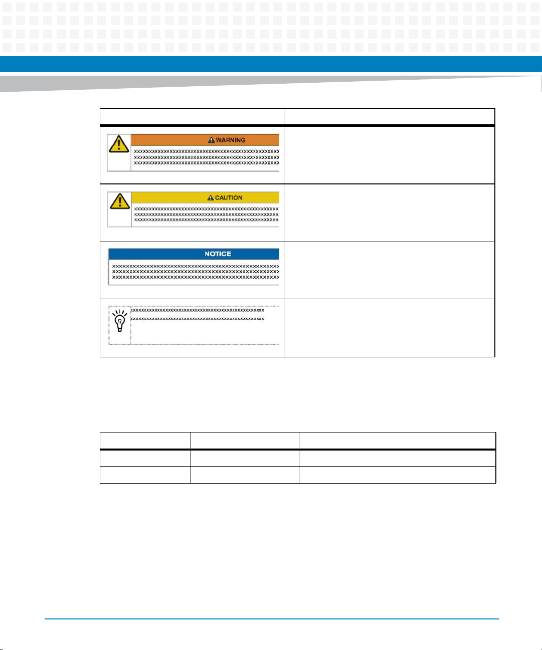
Notation Description
About this Manual
Indicates a hazardous situation which, if not avoided,
could result in death or serious injury
Indicates a hazardous situation which, if not avoided,
may result in minor or moderate injury
Indicates a property damage message
No danger encountered. Pay attention to important
information
Summary of Changes
This manual has been revised and replaces all prior editions.
Part Number Publication Date Description
6806800R95A August, 2013
6806800R95B August, 2014 Re-branded to Artesyn
14
Initial version
COMX-P40x0 ENP2 Installation and Use (6806800R95B)
Page 15

Introduction
1.1 Overview
The COMX-P40x0 ENP2 is a COM Express module based on the Freescale Power PC P4040 and
P4080 platforms. This board provides some of the universal interfaces such as Gigabit
Ethernet, USB, PCIE, and so on.
Following are the features of the COMX-P40x0 ENP2:
Form Factor: Basic (95mm x 125mm)
P4040 or P4080 CPU supported
Boot Options:
– 16 bit NOR FLASH from local bus (standard product default)
– NAND FLASH from local bus
– I2C EEPROM
Chapter 1
Note: Selectable via carrier
Demo, runtime Linux Operating System and filesystem(s), pre-installed in NOR/NAND
Flash.
Dual channel on-board DDR3 with ECC. COMX-P40x0-2G boards have 1GB per channel for
a total of 2GB. COMX-P40x0-4G boards have 2GB per channel for a total of 4GB.
– Designed to support up to 8GB of DDR3
16 lanes of SERDES routed to COME connectors, which can be configured as PCIE, XAUI,
SRIO, SGMII
4 UARTs (2-wire interfaces)
0/1/2 GE ports (option available to use this port as USB)
5/4/0 USB ports
IEEE 1588 support signals to the COME connectors
Total 3 I2C buses
1 SPI bus with 3 chip select signals
Secure Digital Host Controller interface to the COME connector for MultiMediaCard
(MMC) and Secure Digital card (SD) support.
COMX-P40x0 ENP2 Installation and Use (6806800R95B)
15
Page 16
Introduction
Tamper detect pin to the COME connectors
On-board RTC and WDT device
Provide both remote and local thermal sensor
JTAG connector on module
Aurora testing points on module
12V power supplied to module through COME connectors
5V standby power from COME connector not required/used by module
Due to P4080 errata GEN-A009, Aurora ports are disabled by default in RCW and must be
re-enabled for debug. For assistance, contact Artesyn representative.
1.2 Standard Compliances
The product is designed to meet the following standards.
Table 1-1 Standard Compliances
Standard Description
UL60950-1 EN 60950-1 IEC
60950-1 CAN/CSA C22.2 No
60950-1
UL/CSA 60950-1
EN 60950-1
IEC 60950-1 CB Scheme
FCC 47 CFR Part 15 Subpart B
(US), Class A
EN55022 Class A (EU)
AS/NZS CISPR 22 Class A
(Australia/New Zealand)
VCCI Class A (Japan)
16
Safety Requirements
Legal safety requirements
EMC requirements (legal) on system level
(predefined Artesyn system)
COMX-P40x0 ENP2 Installation and Use (6806800R95B)
Page 17
Table 1-1 Standard Compliances (continued)
Standard Description
CISPR 22 CISPR 24 EN55022 EN
55024
ETSI EN 300 019 Series Environmental Requirement
Directive 2011/65/EU Directive on the restriction of the use of certain
EMC Requirements on system level
hazardous substances in electrical and electronic
equipment (ROHS)
Introduction
COMX-P40x0 ENP2 Installation and Use (6806800R95B)
17
Page 18
Introduction
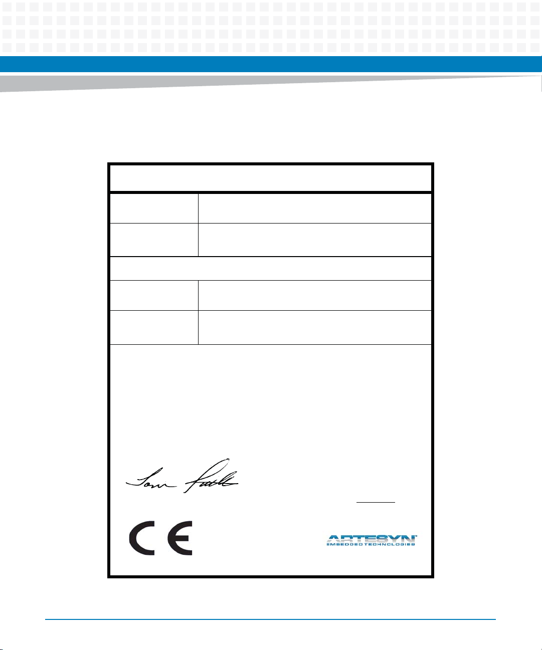
The following figure contains the declaration of conformity for COMX-P40x0.
Figure 1-1 Declaration of Conformity
E
C Declaration of Conformity
According to EN 17050-1:2004
Manufacturer’s Name:
Manufacturer’s Address:
Declares that the following product, in accordance with the requirements of 2004/108/EC, 2006/95/EC,
2011/65/EU and their amending directives,
Product:
Artesyn Embedded Technologies
Embedded Computing
Zhongshan General Carton Box Factory Co. Ltd. No 62, Qi
Guan Road West, Shiqi District, 528400 Zhongshan City
Guangdong, PRC
COMX-P40x0-ENP2—Express Form Factor Processor Pluggable Mezzanine Module For Extended Temperature and rugged Environments
Model Name/Number:
has been designed and manufactured to the following specifications:
EN55022: 2010 Class B
EN55024: 2010
IEC 60950-1: 2005 (2nd Edition) + A1: 2009
2011/65/EU RoHS Directive
As manufacturer we hereby declare that the product named above has been designed to comply with the relevant sections of the above referenced specifications. This product complies with the essential health and safety
requirements of the above specified directives. We have an internal production control system that ensures
compliance between the manufactured products and the technical documentation.
___________________________________________________ ___
Tom Tuttle, Manager, Product Testing Services Date (MM/DD/YYYY)
COMX-P40x0-ENP2, SCP-P4040-4G-ENP2, COMX-P4040-4G-ENP2,
COMX-P4080-2G-ENP2, COMX-P4080-4G-E-ENP2
07/30/2014
______
18
COMX-P40x0 ENP2 Installation and Use (6806800R95B)
Page 19
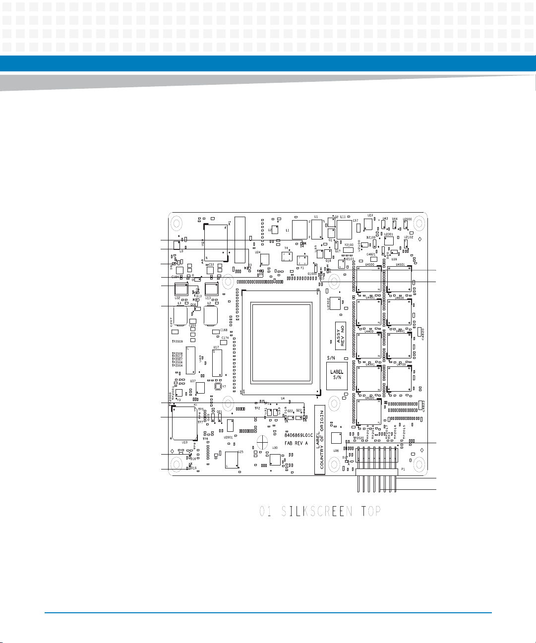
1.3 Mechanical Data
This section provides mechanical details of COMX-P4080-ENP2 and COMX-P4040-ENP2
boards.
Figure 1-2 COMX-P40X0-ENP2 Top View
D4:3.3V power ok
D3:system asleep
D6:1.8V power ok
D5:2.5V power ok
D9:Platform Power OK
D13:CORE power ok
Introduction
D7:DDR3 power ok
D10:1.5V power ok
Debug led D19
Debug led D18
D16:USB hub High Speed
D15:USB hub Active
COMX-P40x0 ENP2 Installation and Use (6806800R95B)
Thermal issue D17
Pin 1
COP header
19
Page 20
Introduction
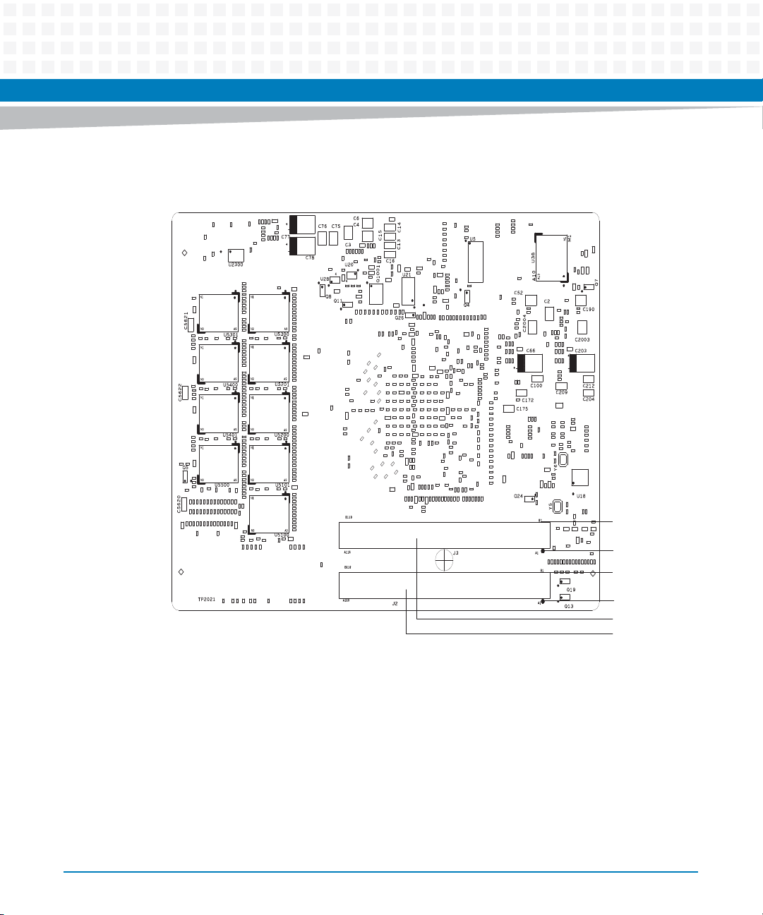
Figure 1-3 COMX-P40X0-ENP2 Bottom View
20
PIN B1
PIN A1
PIN B1
PIN A1
COME: CD: J3
COME: AB: J2
COMX-P40x0 ENP2 Installation and Use (6806800R95B)
Page 21
1.3.1 COMX-P4080 ENP2
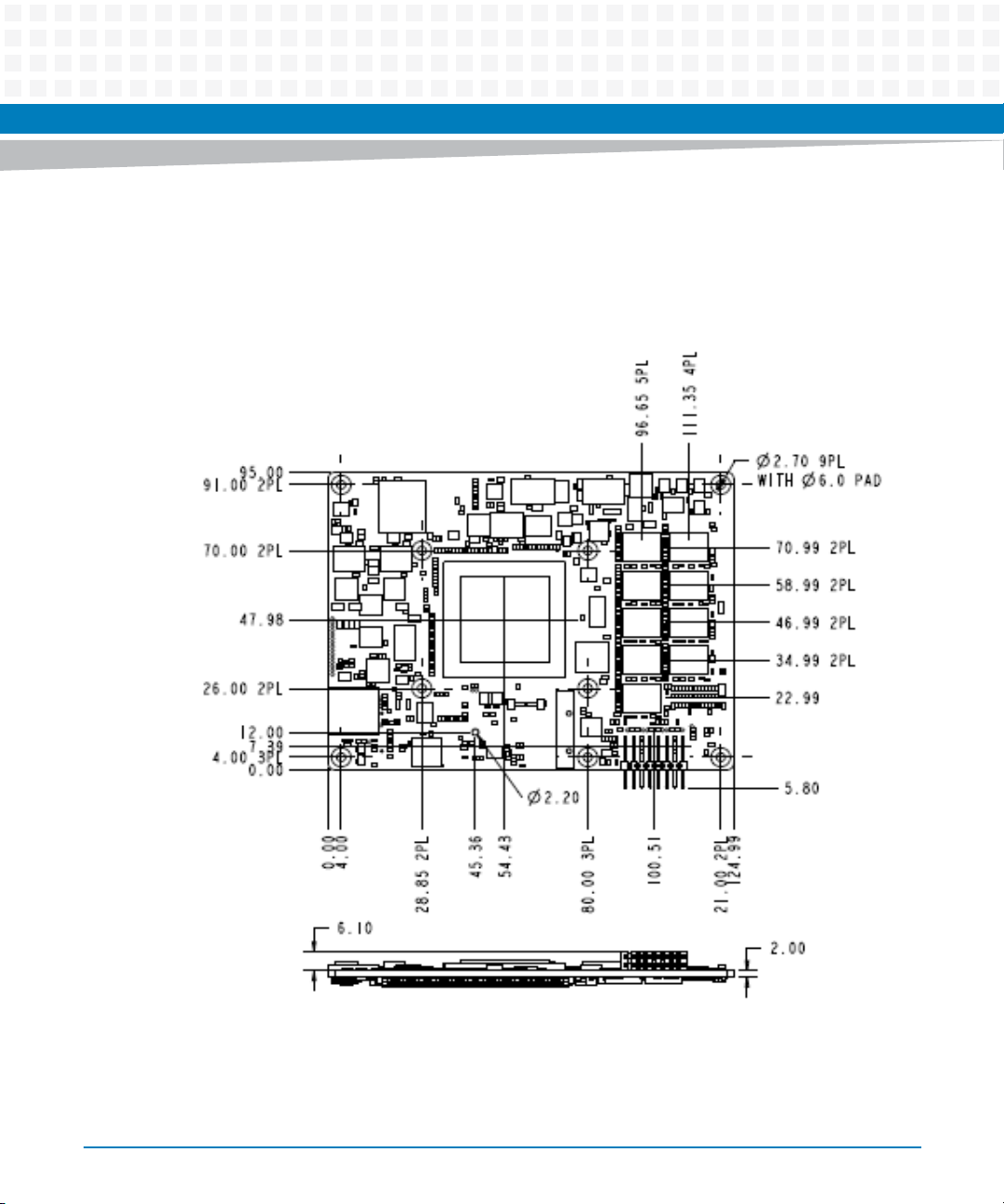
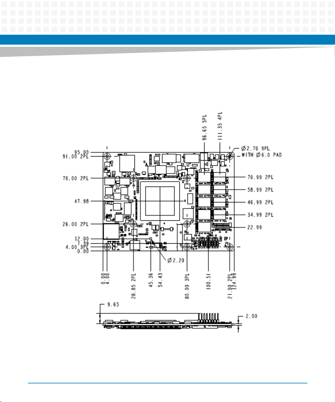
The following figure illustrates the top and side views of the COMX-P4080 ENP2 board.
Figure 1-4 COMX-P4080 ENP2 Mechanical Dimensions (Top and side views)
Introduction
COMX-P40x0 ENP2 Installation and Use (6806800R95B)
21
Page 22
Introduction
Table 1-2 COMX-P4080 ENP2 PCB Dimensions
Characteristic Value
Length 125 mm
Width 95 mm
PCB Thickness 2 mm
Mounting height top side (component side 1) 6.1 mm
22
COMX-P40x0 ENP2 Installation and Use (6806800R95B)
Page 23
1.3.2 COMX-P4040 ENP2
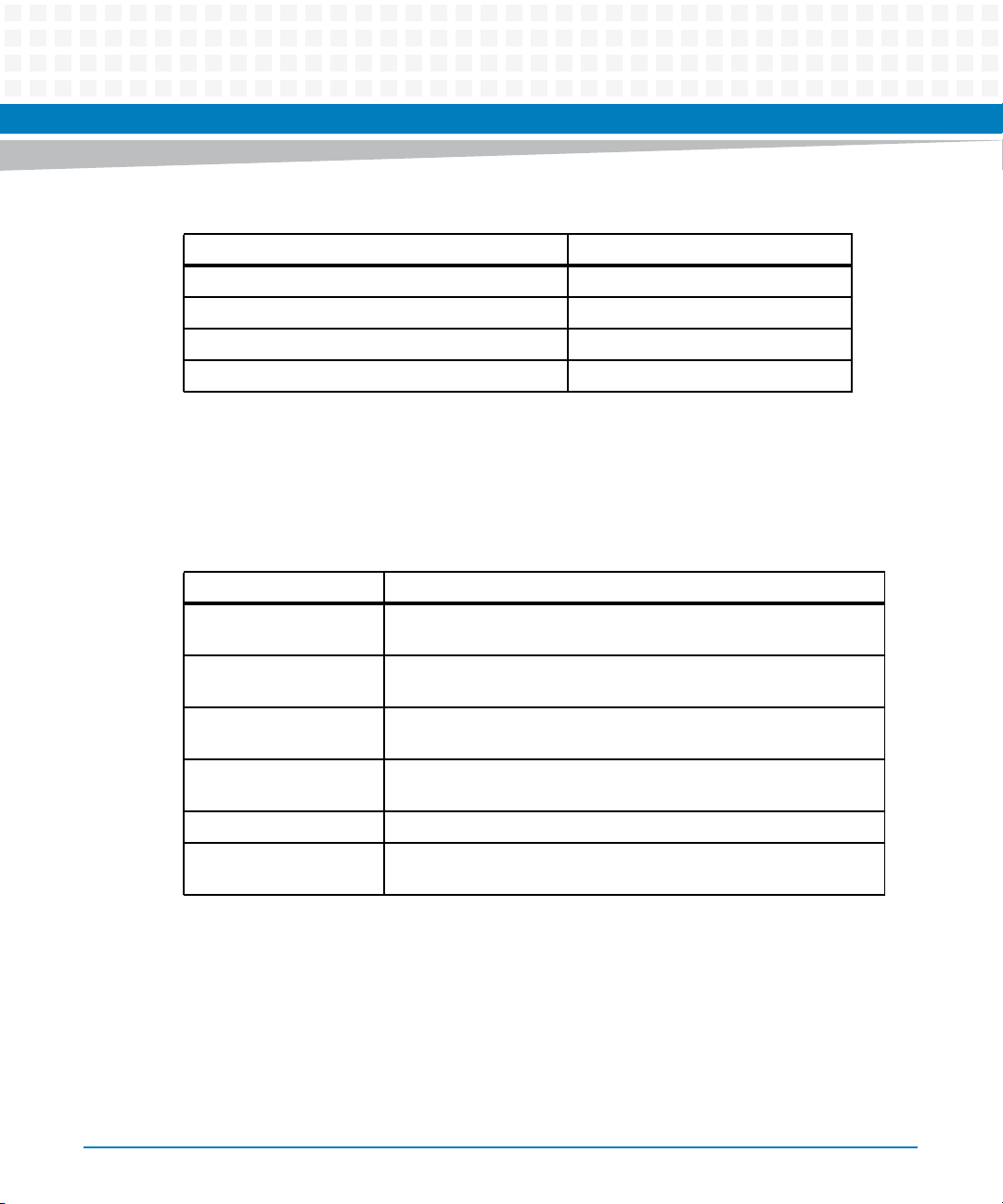
The following figure illustrates the top and side views of the COMX-P4040 ENP2 board.
Figure 1-5 COMX-P4040 ENP2 Mechanical Dimensions (Top and side views)
Introduction
COMX-P40x0 ENP2 Installation and Use (6806800R95B)
23
Page 24
Introduction
Table 1-3 COMX-P4040 ENP2 PCB Dimensions
Characteristic Value
Length 125 mm
Width 95 mm
PCB Thickness 2 mm
Mounting height top side (component side 1) 9.65 mm
1.4 Ordering Information
Use the order numbers below when ordering product variants.
Table 1-4 Ordering Information
Order Number Description
COMX-P4080-2G-ENP2 QorIQ P4080 with 2GB DDR3, 0 Gigabit Ethernet, 5 USB ports. COM
Express Basic size.
COMX-P4080-4G-E-ENP2 QorIQ P4080 with 4GB DDR3, 1 Gigabit Ethernet, 4 USB ports. COM
Express Basic Size.
COMX-P4040-4G-ENP2 QorIQ P4040 with 4GB DDR3, 1 Gigabit Ethernet, 4 USB ports. COM
Express Basic Size.
SCP-P4040-4G-ENP2 QorIQ P4040 with 4GB DDR3, 1 Gigabit Ethernet, 4 USB ports. COM
Express Basic Size.
COMX-CAR-P1 Artesyn DEVELOPMENT CARRIER FOR QORIQ MODULES.
COMX-P4000-ENPHTSNK
Heatsink for COMX-P40x0 ENP2 module.
1.5 Product Identification
This section shows the serial number and its location on the COMX-P4080 ENP2 and COMXP4040 ENP2 boards.
24
COMX-P40x0 ENP2 Installation and Use (6806800R95B)
Page 25
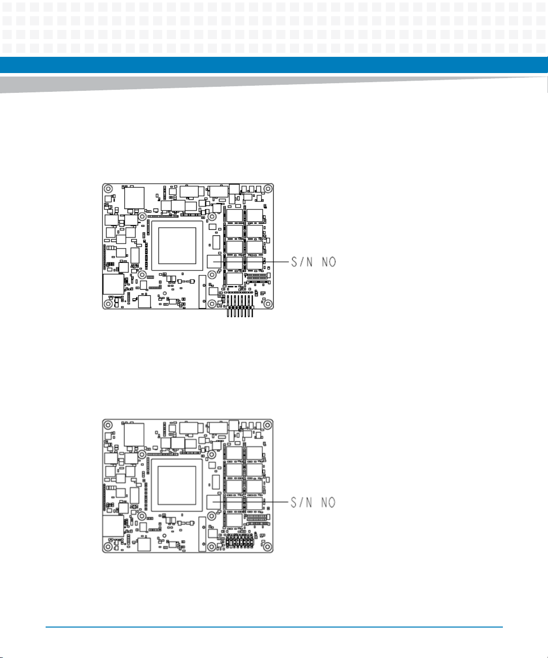
1.5.1 COMX-P4080 ENP2
The following figure shows the location of serial number on COMX-P4080 ENP2 board.
Figure 1-6 COMX-P4080 ENP2 Serial Number Location
Introduction
1.5.2 COMX-P4040 ENP2
The following figure shows the location of serial number on COMX-P4040 ENP2 board.
Figure 1-7 COMX-P4040 ENP2 Serial Number Location
COMX-P40x0 ENP2 Installation and Use (6806800R95B)
25
Page 26

Introduction
26
COMX-P40x0 ENP2 Installation and Use (6806800R95B)
Page 27
Hardware Preparation and Installation
2.1 Environmental and Power Requirements
2.1.1 Environmental Requirements
The following module environmental requirements must not be exceeded.
Operating temperature refers to the temperature of the air circulating around the module
and not the component temperature.
The following table provides the environmental requirements for the module.
Chapter 2
Table 2-1 Environmental Requirements
Requirement Operating Non-Operating
Temperature
Humidity
Vibration Sine (10mins/axis) 5G, 15 to 2000Hz
Vibration Random (1hr/axis) 0.04g2/Hz, 15 to 2000Hz
Shock 30g/11mS(half sine)
Altitude -60 to 4000 m ASL
Thermal Requirements
A standard passive heat sink can be provided by Artesyn; 12 CFM system airflow volume (at
71oC) is needed for the heat sink to keep sufficient cooling to the module. Contact your
Artesyn sales representative for detailed thermal information.
-40°C to +71°C
to 100% RH
(8GRMS)
-50°C to +100°C
to 100% RH
COMX-P40x0 ENP2 Installation and Use (6806800R95B)
27
Page 28
Hardware Preparation and Installation
The following table summarizes components that exhibited significant temperature rises and
their maximum allowable operating temperature. These components should be monitored in
order to assess thermal performance during customized thermal solution development.
Table 2-2 Critical Temperature Spots
Component Identifier Heat Dissipation Power (W) Maximum Allowable Temperature (°C)
CPU: P4080 20.5 CPU: 105 (Tj)
CPU: P4040 16.8 CPU: 105 (Tj)
Memory SDRAM 3 95 (Tc)
GbE Transceiver:
BCM5482
Row 4, Note: For modules with Gigabit Ethernet port options.
0.86 125 (Tj)
System Overheating
Improper cooling can lead to system damage and void the manufacturer's warranty.
Personal Injury
During operation, hot surfaces may be present on the heat sinks and the components of the
product.
To prevent injury, do not touch any of the exposed components or heatsinks on the product
when handling.
28
COMX-P40x0 ENP2 Installation and Use (6806800R95B)
Page 29
Hardware Preparation and Installation
Power Requirements
This board is designed to operate with the input voltages and currents as defined in the
following tables.
Table 2-3 Current Drawn
State 12v VCC_RTC
Idle 2.81A 100 uA
Full Loading (Linux) 2.91A 100 uA
Table 2-4 COMX-P4080-4G-E-ENP2
Volts Amps Power
12 2.6 31.2
Total Power dissipation (W) 31.2
2.2 Unpacking and Inspecting the Enclosure
Read all notices and cautions prior to unpacking the product.
Damage of Circuits
Electrostatic discharge and incorrect installation/removal of the product can damage
circuits or shorten their life.
Before touching the product make sure that you are working in an ESD-safe
environment with protective equipment such an ESD wrist strap and ESD shoes. Hold
the product by its edges and do not touch any components or circuits.
COMX-P40x0 ENP2 Installation and Use (6806800R95B)
29
Page 30
Hardware Preparation and Installation
Shipment Inspection
1. Verify that you have received all items of your shipment.
Printed Quick Start Guide and Safety Notes
COMX-P40x0 ENP2 Module
2. Check for damage and report any damage or differences to customer service.
3. Remove the desiccant bag shipped together with the enclosure and dispose of it
according to your country’s legislation.
Improperly disposing of used products may harm the environment.
Always dispose of used products according to your country’s legislation and manufacturer’s
instructions.
The product is thoroughly inspected before shipment. If any damage occurred during
transportation or any items are missing, contact customer service immediately.
2.3 Installing and Removing the Module on the Carrier Board
The heat sink is assembled to the module before the procedure below:
Installing the COM module on the carrier board
1. Line up the board-to-board connector of the module assembly with the board-to-board
connector of the carrier board.
2. Make sure that the inter-connectors are properly aligned and that the five standoffs on the
module have contact with the top of the carrier board.
30
COMX-P40x0 ENP2 Installation and Use (6806800R95B)
Page 31

Hardware Preparation and Installation
3. From the bottom side of the carrier, locate the screw holes corresponding to the module
standoffs.
4. Use the screws to fasten the module to the carrier board.
Removing the module from the carrier board
1. From the back side of the carrier, locate the five screws that connect the module assembly
to the carrier board.
2. Loosen and remove the screws.
3. While holding the edges, pull the module from the carrier board.
COMX-P40x0 ENP2 Installation and Use (6806800R95B)
31
Page 32

Hardware Preparation and Installation
The figure below illustrates the screw-holes for mounting the module on carrier board.
Figure 2-1 Mounting Module on Carrier Board
32
This installation/removal procedure is only for reference. Assemble the heatsink and the
module based on your own thermal solution.
COMX-P40x0 ENP2 Installation and Use (6806800R95B)
Page 33

Hardware Preparation and Installation
Heat-sink Installation
The following figures illustrate the heat-sink installation on the module:
Figure 2-2 Heat-sink installation
COMX-P40x0 ENP2 Installation and Use (6806800R95B)
33
Page 34

Hardware Preparation and Installation
Figure 2-2 Heat-sink installation (continued)
34
COMX-P40x0 ENP2 Installation and Use (6806800R95B)
Page 35

Controls, LEDs, and Connectors
3.1 Connectors and Switches
3.1.1 On-Board Connectors
P4080 COP Header
The following table lists the pin-out of the COP (Common On-Chip Processor) header for
modules with the P4080 CPU.
Table 3-1 P4080 COP Header Pin-out
Pin Signal Name
1 GND
2 cpu_ckstp_out_n
Chapter 3
3 key for p4040 cop nc for
P4080
4 cop_hrst_n
5empty
6 cop_srst_n
7NC
8TMS
9 NC (CKSTP INPUT)
10 TCK
11 VDDSENSE (+3.3V)
12 NC (RUNSTOP)
13 TRST#
14 cpujtag_tdi
15 empty 10k pullup
16 cpujtag_tdo
COMX-P40x0 ENP2 Installation and Use (6806800R95B)
35
Page 36

Controls, LEDs, and Connectors
P4040 COP Header
The following table lists the pin-out of the COP header for modules with the P4040 CPU.
Table 3-2 P4040 COP Header Pin-out
Pin Signal Name
1 cpujtag_tdo
2 empty 10k pullup
3 cpujtag_tdi
4TRST#
5 NC (RUNSTOP)
6 VDDSENSE (+3.3V)
7TCK
8 NC (CKSTP INPUT)
9TMS
10 NC
11 cop_srst_n
12 empty
13 cop_hrst_n
14 key for p4040 cop nc for
P4080
15 cpu_ckstp_out_n
16 GND
36
COMX-P40x0 ENP2 Installation and Use (6806800R95B)
Page 37

3.1.2 ON-BOARD LEDS
There are several status LEDs provided on the module. The following table lists the LED
functions.
Table 3-3 Module LED Status
LED Status
D17 Thermal issue
D18~D19 Debug LED 1~2
D3 System asleep
D7 DDR3 power OK
D4 3.3V power OK
D5 2.5V power OK
D6 1.8V power OK
Controls, LEDs, and Connectors
D13 CORE power OK
D9 PLATFORM power OK
D10 1.5V power OK
D15 USB hub 2 active
D16 USB hub 2 high speed
D1, D2, D15, D16 are for modules with USB port options.
3.1.3 COMX AB-CD Connectors
The following table lists the pin-out of the AB- CD COMX connectors for the P40x0 COMX
modules:
Table 3-4 COMX AB-CD Connectors
Connector
refdes
J2 AB1 A1 GND
J2 AB1 A2 LAN1_MDI_N<3> bidir
Connector
name Pin Net Name
direction from
COMX notes
COMX-P40x0 ENP2 Installation and Use (6806800R95B)
37
Page 38

Controls, LEDs, and Connectors
Table 3-4 COMX AB-CD Connectors (continued)
Connector
refdes
J2 AB1 A3 LAN1_MDI_P<3> bidir
J2 AB1 A4 LAN1_LINK100_N out Lan1 link 100 active
J2 AB1 A5 LAN1_LINK1000_N out lan1 link 1000 active
J2 AB1 A6 LAN1_MDI_N<2 bidir
J2 AB1 A7 LAN1_MDI_P<2 bidir
J2 AB1 A8 LAN1_LINK_N out out from comx
J2 AB1 A9 LAN1_MDI_N<1> bidir
J2 AB1 A10 LAN1_MDI_P<1> bidir
J2 AB1 A11 GND
J2 AB1 A12 LAN1_MDI_N<0> bidir
J2 AB1 A13 LAN1_MDI_P<0> bidir
J2 AB1 A14 V1P8_CTRL out out from comx 1.8v
J2 AB1 A15 N/C
J2 AB1 A16 N/C
Connector
name Pin Net Name
direction from
COMX notes
low
low
power indicator
J2 AB1 A17 N/C
J2 AB1 A18 N/C
J2 AB1 A19 N/C
J2 AB1 A20 N/C
J2 AB1 A21 GND
J2 AB1 A22 N/C
J2 AB1 A23 N/C
J2 AB1 A24 N/C
J2 AB1 A25 N/C
J2 AB1 A26 N/C
38
COMX-P40x0 ENP2 Installation and Use (6806800R95B)
Page 39

Table 3-4 COMX AB-CD Connectors (continued)
Controls, LEDs, and Connectors
Connector
refdes
J2 AB1 A27 N/C
J2 AB1 A28 N/C
J2 AB1 A29 POVDD_EN_KEY in Power ON Enable
J2 AB1 A30 LBC_CS_KEY in Local Bus Control
J2 AB1 A31 GND
J2 AB1 A32 N/C
J2 AB1 A33 N/C
J2 AB1 A34 N/C
J2 AB1 A35 N/C
J2 AB1 A36 N/C
J2 AB1 A37 N/C
J2 AB1 A38 N/C
J2 AB1 A39 N/C
J2 AB1 A40 N/C
J2 AB1 A41 GND
Connector
name Pin Net Name
direction from
COMX notes
Chipselect key
J2 AB1 A42 USB2_N bidir
J2 AB1 A43 USB2_P bidir
J2 AB1 A44 USB_OC_2_3_N in
J2 AB1 A45 USB0_N bidir
J2 AB1 A46 USB0_P bidir
J2 AB1 A47 V3P3_BAT 3.3v battery power
J2 AB1 A48 USB2_PWREN out
J2 AB1 A49 USB0_PWREN out
J2 AB1 A50 USB5_PWREN out
J2 AB1 A51 GND
J2 AB1 A52 SERDES_TX5_P out
COMX-P40x0 ENP2 Installation and Use (6806800R95B)
39
Page 40

Controls, LEDs, and Connectors
Table 3-4 COMX AB-CD Connectors (continued)
Connector
refdes
J2 AB1 A53 SERDES_TX5_N out
J2 AB1 A54 CPU_SDHC_DAT0 bidir
J2 AB1 A55 SERDES_TX4_P out
J2 AB1 A56 SERDES_TX4_N out
J2 AB1 A57 GND
J2 AB1 A58 SERDES_TX3_P out
J2 AB1 A59 SERDES_TX3_N out
J2 AB1 A60 GND
J2 AB1 B1 GND
J2 AB1 B2 LAN1_ACTIVITY_N out lan1 activity
J2 AB1 B3 TSEC_1588_CLK_OUT out
J2 AB1 B4 TSEC_1588_PULSE_OUT1 out
J2 AB1 B5 TSEC_1588_PULSE_OUT2 out
J2 AB1 B6 TSEC_1588_ALARM_OUT1 out
J2 AB1 B7 TSEC_1588_ALARM_OUT2 out
Connector
name Pin Net Name
direction from
COMX notes
J2 AB1 B8 TSEC_1588_TRIG_IN1 in
J2 AB1 B9 TSEC_1588_TRIG_IN2 in
J2 AB1 B10 TSEC_1588_CLK_IN1 in
J2 AB1 B11 GND
J2 AB1 B12 N/C
J2 AB1 B13 N/C
J2 AB1 B14 N/C
J2 AB1 B15 N/C
J2 AB1 B16 N/C
J2 AB1 B17 N/C
40
COMX-P40x0 ENP2 Installation and Use (6806800R95B)
Page 41

Table 3-4 COMX AB-CD Connectors (continued)
Controls, LEDs, and Connectors
Connector
refdes
J2 AB1 B18 N/C
J2 AB1 B19 N/C
J2 AB1 B20 N/C
J2 AB1 B21 GND
J2 AB1 B22 N/C
J2 AB1 B23 N/C
J2 AB1 B24 N/C
J2 AB1 B25 N/C
J2 AB1 B26 N/C
J2 AB1 B27 WDT_OUT_N out Watch dog Timer Out
J2 AB1 B28 LBC_WE1_N out P40x0 local bus
J2 AB1 B29 N/C
J2 AB1 B30 N/C
J2 AB1 B31 GND
J2 AB1 B32 LBC_LGPL5 in
Connector
name Pin Net Name
direction from
COMX notes
LWE1_N
J2 AB1 B33 CPU_IIC1_CLK bidir
J2 AB1 B34 CPU_IIC1_DAT bidir
J2 AB1 B35 N/C
J2 AB1 B36 N/C
J2 AB1 B37 N/C
J2 AB1 B38 USB_OC_4_5_N in
J2 AB1 B39 USB5_N bidir
J2 AB1 B40 USB5_P bidir
J2 AB1 B41 GND
J2 AB1 B42 USB3_N bidir
J2 AB1 B43 USB3_P bidir
COMX-P40x0 ENP2 Installation and Use (6806800R95B)
41
Page 42

Controls, LEDs, and Connectors
Table 3-4 COMX AB-CD Connectors (continued)
Connector
refdes
J2 AB1 B44 USB_OC_0_1_N in
J2 AB1 B45 USB1_N bidir
J2 AB1 B46 USB1_P bidir
J2 AB1 B47 USB3_PWREN out
J2 AB1 B48 USB1_PWREN out
J2 AB1 B49 RESET_BUTTON_N in
J2 AB1 B50 CB_RESET_GPIO20_N out
J2 AB1 B51 GND
J2 AB1 B52 SERDES_RX5_P in
J2 AB1 B53 SERDES_RX5_N in
J2 AB1 B54 CPU_SDHC_CMD bidir
J2 AB1 B55 SERDES_RX4_P in
J2 AB1 B56 SERDES_RX4_N in
J2 AB1 B57 CPU_SDHC_WP in
J2 AB1 B58 SERDES_RX3_P in
J2 AB1 B59 SERDES_RX3_N in
Connector
name Pin Net Name
direction from
COMX notes
J2 AB1 B60 GND
J2 AB2 A61 SERDES_TX2_P out
J2 AB2 A62 SERDES_TX2_N out
J2 AB2 A63 CPU_SDHC_DAT1 bidir
J2 AB2 A64 SERDES_TX1_P out
J2 AB2 A65 SERDES_TX1_N out
J2 AB2 A66 GND
J2 AB2 A67 CPU_SDHC_DAT2 bidir
J2 AB2 A68 SERDES_TX0_P out
42
COMX-P40x0 ENP2 Installation and Use (6806800R95B)
Page 43

Table 3-4 COMX AB-CD Connectors (continued)
Controls, LEDs, and Connectors
Connector
refdes
J2 AB2 A69 SERDES_TX0_N out
J2 AB2 A70 GND
J2 AB2 A71 N/C
J2 AB2 A72 N/C
J2 AB2 A73 N/C
J2 AB2 A74 N/C
J2 AB2 A75 N/C
J2 AB2 A76 N/C
J2 AB2 A77 N/C
J2 AB2 A78 N/C
J2 AB2 A79 N/C
J2 AB2 A80 GND
J2 AB2 A81 N/C
J2 AB2 A82 N/C
J2 AB2 A83 CPU_IIC2_CLK bidir
J2 AB2 A84 CPU_IIC2_DAT bidir
Connector
name Pin Net Name
direction from
COMX notes
J2 AB2 A85 CPU_SDHC_DAT3 bidir
J2 AB2 A86 N/C
J2 AB2 A87 N/C
J2 AB2 A88 CLK_125M_100M_COME_
SDREF1_P
J2 AB2 A89 CLK_125M_100M_COME_
SDREF1_N
J2 AB2 A90 GND
J2 AB2 A91 CPU_SPI_CS0_K_N out
J2 AB2 A92 CPU_SPI_MISO in
J2 AB2 A93 CPU_SDHC_CLK out
COMX-P40x0 ENP2 Installation and Use (6806800R95B)
out
out
43
Page 44

Controls, LEDs, and Connectors
Table 3-4 COMX AB-CD Connectors (continued)
Connector
refdes
J2 AB2 A94 CPU_SPI_CLK_COME out
J2 AB2 A95 CPU_SPI_MOSI out
J2 AB2 A96 GND
J2 AB2 A97 V12
J2 AB2 A98 V12
J2 AB2 A99 V12
J2 AB2 A100 GND
J2 AB2 A101 V12
J2 AB2 A102 V12
J2 AB2 A103 V12
J2 AB2 A104 V12
J2 AB2 A105 V12
J2 AB2 A106 V12
J2 AB2 A107 V12
J2 AB2 A108 V12
J2 AB2 A109 V12
Connector
name Pin Net Name
direction from
COMX notes
J2 AB2 A110 GND
J2 AB2 B61 SERDES_RX2_P in
J2 AB2 B62 SERDES_RX2_N in
J2 AB2 B63 CPU_SDHC_CD bi
J2 AB2 B64 SERDES_RX1_P in
J2 AB2 B65 SERDES_RX1_N in
J2 AB2 B66 N/C
J2 AB2 B67 CPU_HRESE T_COME_N in Only used on P4080-2G
assembly
J2 AB2 B68 SERDES_RX0_P in
44
COMX-P40x0 ENP2 Installation and Use (6806800R95B)
Page 45

Table 3-4 COMX AB-CD Connectors (continued)
Controls, LEDs, and Connectors
Connector
refdes
J2 AB2 B69 SERDES_RX0_N in
J2 AB2 B70 GND
J2 AB2 B71 N/C
J2 AB2 B72 N/C
J2 AB2 B73 N/C
J2 AB2 B74 N/C
J2 AB2 B75 N/C
J2 AB2 B76 N/C
J2 AB2 B77 N/C
J2 AB2 B78 N/C
J2 AB2 B79 N/C
J2 AB2 B80 GND
J2 AB2 B81 N/C
J2 AB2 B82 N/C
J2 AB2 B83 N/C
J2 AB2 B84 V5SB
Connector
name Pin Net Name
direction from
COMX notes
J2 AB2 B85 V5SB
J2 AB2 B86 V5SB
J2 AB2 B87 V5SB
J2 AB2 B88 CPU_SPI_CS1_N out
J2 AB2 B89 N/C
J2 AB2 B90 GND
J2 AB2 B91 N/C
J2 AB2 B92 N/C
J2 AB2 B93 N/C
J2 AB2 B94 N/C
COMX-P40x0 ENP2 Installation and Use (6806800R95B)
45
Page 46

Controls, LEDs, and Connectors
Table 3-4 COMX AB-CD Connectors (continued)
Connector
refdes
J2 AB2 B95 CPU_IIC4_CLK bidir
J2 AB2 B96 CPU_IIC4_DAT bidir
J2 AB2 B97 BANK1_SEL_FS0 in
J2 AB2 B98 BANK2_SEL_S1 in
J2 AB2 B99 BANK3_SEL_S1 in
J2 AB2 B100 GND
J2 AB2 B101 V12
J2 AB2 B102 V12
J2 AB2 B103 V12
J2 AB2 B104 V12
J2 AB2 B104 V12
J2 AB2 B106 V12
J2 AB2 B107 V12
J2 AB2 B108 V12
J2 AB2 B109 V12
J2 AB2 B110 GND
Connector
name Pin Net Name
direction from
COMX notes
J3 CD1 A1 GND
J3 CD1 A2 LAN2_ACTIVITY_N in
J3 CD1 A3 LAN2_MDI_N<3> bidir
J3 CD1 A4 LAN2_MDI_P<3> bidir
J3 CD1 A5 LAN2_LINK100_N in
J3 CD1 A6 LAN2_MDI_N<2> bidir
J3 CD1 A7 LAN2_MDI_P<2> bidir
J3 CD1 A8 LAN2_LINK1000_N in
J3 CD1 A9 LAN2_MDI_N<1> bidir
46
COMX-P40x0 ENP2 Installation and Use (6806800R95B)
Page 47

Table 3-4 COMX AB-CD Connectors (continued)
Controls, LEDs, and Connectors
Connector
refdes
J3 CD1 A10 LAN2_MDI_P<1> bidir
J3 CD1 A11 GND
J3 CD1 A12 LAN2_MDI_N<0> bidir
J3 CD1 A13 LAN2_MDI_P<0> bidir
J3 CD1 A14 LAN2_LINK_N in
J3 CD1 A15 LBC_LAD<8> bidir
J3 CD1 A16 LBC_LAD<9> bidir
J3 CD1 A17 LBC_CLE_N out
J3 CD1 A18 LBC_FCMALE_N out
J3 CD1 A19 SERDES_RX6_P in
J3 CD1 A20 SERDES_RX6_N in
J3 CD1 A21 GND
J3 CD1 A22 SERDES_RX7_P in
J3 CD1 A23 SERDES_RX7_N in
J3 CD1 A24 N/C
J3 CD1 A25 LBC_LAD<10> bidir
Connector
name Pin Net Name
direction from
COMX notes
J3 CD1 A26 LBC_LAD<11> bidir
J3 CD1 A27 LBC_LAD<12> bidir
J3 CD1 A28 LBC_LAD<13> bidir
J3 CD1 A29 LBC_LAD<14> bidir
J3 CD1 A30 LBC_LAD<15> bidir
J3 CD1 A31 GND
J3 CD1 A32 CPU_UART1_SOUT out
J3 CD1 A33 CPU_UART1_SIN in
J3 CD1 A34 CPU_UART1_CTS out Not used
J3 CD1 A35 CPU_UART1_RTS in Not used
COMX-P40x0 ENP2 Installation and Use (6806800R95B)
47
Page 48

Controls, LEDs, and Connectors
Table 3-4 COMX AB-CD Connectors (continued)
Connector
refdes
J3 CD1 A36 CPU_UART2_SOUT out
J3 CD1 A37 CPU_UART2_SIN in
J3 CD1 A38 CPU_UART2_CTS out Not used
J3 CD1 A39 CPU_UART2_RTS in Not used
J3 CD1 A40 EMI1_MDIO bidir
J3 CD1 A41 GND
J3 CD1 A42 CPU_UART3_SOUT out
J3 CD1 A43 CPU_UART3_SIN in
J3 CD1 A44 N/C
J3 CD1 A45 N/C
J3 CD1 A46 CPU_UART4_SOUT out
J3 CD1 A47 CPU_UART4_SIN in
J3 CD1 A48 N/C
J3 CD1 A49 N/C
J3 CD1 A50 EMI1_MDC_COME out
J3 CD1 A51 GND
Connector
name Pin Net Name
direction from
COMX notes
J3 CD1 A52 SERDES_RX16_P in
J3 CD1 A53 SERDES_RX16_N in
J3 CD1 A54 COME_TYPE0_N out
J3 CD1 A55 SERDES_RX17_P in
J3 CD1 A56 SERDES_RX17_N in
J3 CD1 A57 COME_TYPE1_N out
J3 CD1 A58 SERDES_RX18_P in
J3 CD1 A59 SERDES_RX18_N in
J3 CD1 A60 GND
48
COMX-P40x0 ENP2 Installation and Use (6806800R95B)
Page 49

Table 3-4 COMX AB-CD Connectors (continued)
Controls, LEDs, and Connectors
Connector
refdes
J3 CD1 B1 GND
J3 CD1 B2 N/C
J3 CD1 B3 N/C
J3 CD1 B4 N/C
J3 CD1 B5 N/C
J3 CD1 B6 N/C
J3 CD1 B7 N/C
J3 CD1 B8 N/C
J3 CD1 B9 N/C
J3 CD1 B10 N/C
J3 CD1 B11 GND
J3 CD1 B12 N/C
J3 CD1 B13 N/C
J3 CD1 B14 N/C
J3 CD1 B15 CPU_IRQ_OUT out
J3 CD1 B16 CPU_IRQ0 in
Connector
name Pin Net Name
direction from
COMX notes
J3 CD1 B17 LBC_CLK0 out
J3 CD1 B18 LBC_CLK1 out
J3 CD1 B19 SERDES_TX6_P out
J3 CD1 B20 SERDES_TX6_N out
J3 CD1 B21 GND
J3 CD1 B22 SERDES_TX7_P out
J3 CD1 B23 SERDES_TX7_N out
J3 CD1 B24 LBC_CS6_N out
J3 CD1 B25 LBC_CS3_N out
J3 CD1 B26 LBC_LA<31> bidir
COMX-P40x0 ENP2 Installation and Use (6806800R95B)
49
Page 50

Controls, LEDs, and Connectors
Table 3-4 COMX AB-CD Connectors (continued)
Connector
refdes
J3 CD1 B27 LBC_LA<30> bidir
J3 CD1 B28 LBC_LAD<0> bidir
J3 CD1 B29 LBC_LA<29> bidir
J3 CD1 B30 LBC_LA<28> bidir
J3 CD1 B31 GND
J3 CD1 B32 LBC_LA<27> bidir
J3 CD1 B33 LBC_LA<26> bidir
J3 CD1 B34 LBC_LAD<1> bidir
J3 CD1 B35 LBC_LAD<2> bidir
J3 CD1 B36 LBC_LA<25> bidir
J3 CD1 B37 LBC_LA<24> bidir
J3 CD1 B38 LBC_LA<23> bidir
J3 CD1 B39 LBC_LA<22> bidir
J3 CD1 B40 LBC_LA<21> bidir
J3 CD1 B41 GND
J3 CD1 B42 LBC_LA<20> bidir
Connector
name Pin Net Name
direction from
COMX notes
J3 CD1 B43 LBC_LA<19> bidir
J3 CD1 B44 LBC_LA<18> bidir
J3 CD1 B45 LBC_LAD<3> bidir
J3 CD1 B46 LBC_LAD<4> bidir
J3 CD1 B47 LBC_LAD<5> bidir
J3 CD1 B48 LBC_LAD<6> bidir
J3 CD1 B49 LBC_LAD<7> bidir
J3 CD1 B50 LBC_ALE_N out
J3 CD1 B51 GND
J3 CD1 B52 SERDES_TX16_P out
50
COMX-P40x0 ENP2 Installation and Use (6806800R95B)
Page 51

Table 3-4 COMX AB-CD Connectors (continued)
Controls, LEDs, and Connectors
Connector
refdes
J3 CD1 B53 SERDES_TX16_N out
J3 CD1 B54 COME_TYPE3_N out
J3 CD1 B55 SERDES_TX17_P out
J3 CD1 B56 SERDES_TX17_N out
J3 CD1 B57 COME_TYPE2_N out
J3 CD1 B58 SERDES_TX18_P out
J3 CD1 B59 SERDES_TX18_N out
J3 CD1 B60 GND
J3 CD2 A61 SERDES_RX19_P in
J3 CD2 A62 SERDES_RX19_N in
J3 CD2 A63 CPU_EMI2_MDIO bidir
J3 CD2 A64 GND
J3 CD2 A65 SERDES_RX20_P in
J3 CD2 A66 SERDES_RX20_N in
J3 CD2 A67 LBC_CS5_N out
Connector
name Pin Net Name
direction from
COMX notes
J3 CD2 A68 SERDES_RX21_P in
J3 CD2 A69 SERDES_RX21_N in
J3 CD2 A70 GND
J3 CD2 A71 SERDES_RX22_SATA1_P in
J3 CD2 A72 SERDES_RX22_SATA1_N in
J3 CD2 A73 N/C
J3 CD2 A74 SERDES_RX23_SATA2_P in
J3 CD2 A75 SERDES_RX23_SATA2_N in
J3 CD2 A76 N/C
J3 CD2 A77 LBC_OE_N out
COMX-P40x0 ENP2 Installation and Use (6806800R95B)
51
Page 52

Controls, LEDs, and Connectors
Table 3-4 COMX AB-CD Connectors (continued)
Connector
refdes
J3 CD2 A78 N/C
J3 CD2 A79 N/C
J3 CD2 A80 GND
J3 CD2 A81 LBC_WP_N out
J3 CD2 A82 LBC_RB_N out
J3 CD2 A83 CPU_IRQ1 in
J3 CD2 A84 GND
J3 CD2 A85 CPU_IRQ2 in
J3 CD2 A86 CPU_IRQ3 in
J3 CD2 A87 GND
J3 CD2 A88 CPU_GPI0 in
J3 CD2 A89 CPU_GPI1 in
J3 CD2 A90 GND
J3 CD2 A91 IOEXT_GPI5 in
J3 CD2 A92 CPU_GPI3 in
J3 CD2 A93 GND
Connector
name Pin Net Name
direction from
COMX notes
J3 CD2 A94 CPU_GPI4 in
J3 CD2 A95 IOEXT_GPI6 in
J3 CD2 A96 GND
J3 CD2 A97 IOEXT_GPI7 in
J3 CD2 A98 CPU_SPI_CS2_N out
J3 CD2 A99 CPU_SPI_CS3_N out
J3 CD2 A100 GND
J3 CD2 A101 CLK_125M_100M_COME_
SDREF2_P
J3 CD2 A102 CLK_125M_100M_COME_
SDREF2_N
52
COMX-P40x0 ENP2 Installation and Use (6806800R95B)
out
out
Page 53

Table 3-4 COMX AB-CD Connectors (continued)
Controls, LEDs, and Connectors
Connector
refdes
J3 CD2 A103 GND
J3 CD2 A104 V12
J3 CD2 A105 V12
J3 CD2 A106 V12
J3 CD2 A107 V12
J3 CD2 A108 V12
J3 CD2 A109 V12
J3 CD2 A110 GND
J3 CD2 B61 SERDES_TX19_P out
J3 CD2 B62 SERDES_TX19_N out
J3 CD2 B63 CPU_EMI2_MDC out
J3 CD2 B64 LP_TMP_DET_BAT out
J3 CD2 B65 SERDES_TX20_P out
J3 CD2 B66 SERDES_TX20_N out
J3 CD2 B67 GND
Connector
name Pin Net Name
direction from
COMX notes
J3 CD2 B68 SERDES_TX21_P out
J3 CD2 B69 SERDES_TX21_N out
J3 CD2 B70 GND
J3 CD2 B71 SERDES_TX22_SATA1_P out
J3 CD2 B72 SERDES_TX22_SATA1_N out
J3 CD2 B73 N/C
J3 CD2 B74 SERDES_TX23_SATA2_P out
J3 CD2 B75 SERDES_TX23_SATA2_N out
J3 CD2 B76 GND
J3 CD2 B77 LBC_WE0_N out
COMX-P40x0 ENP2 Installation and Use (6806800R95B)
53
Page 54

Controls, LEDs, and Connectors
Table 3-4 COMX AB-CD Connectors (continued)
Connector
refdes
J3 CD2 B78 LBC_LA<16> bi
J3 CD2 B79 LBC_LA<17> bi
J3 CD2 B80 GND
J3 CD2 B81 LBC_CTL_N out
J3 CD2 B82 LBC_CS4_N out
J3 CD2 B83 CPU_IRQ4 in
J3 CD2 B84 GND
J3 CD2 B85 IOEXT_GPI8 in
J3 CD2 B86 N/C
J3 CD2 B87 GND
J3 CD2 B88 CPU_GPO0 out
J3 CD2 B89 CPU_GPO1 out
J3 CD2 B90 GND
J3 CD2 B91 IOEXT_GPO5 out
J3 CD2 B92 CPU_GPO3 out
J3 CD2 B93 GND
Connector
name Pin Net Name
direction from
COMX notes
J3 CD2 B94 CPU_GPO4 out
J3 CD2 B95 IOEXT_GPO6 out
J3 CD2 B96 GND
J3 CD2 B97 CPU_TMP_DETECT_N in cpu temp detect
J3 CD2 B98 N/C
J3 CD2 B99 N/C
J3 CD2 B100 GND
J3 CD2 B101 P50_LP_TMP_DETECT_GPO7out
J3 CD2 B102 IOEXT_GPO8 out
J3 CD2 B103 GND
54
COMX-P40x0 ENP2 Installation and Use (6806800R95B)
Page 55

Table 3-4 COMX AB-CD Connectors (continued)
Controls, LEDs, and Connectors
Connector
refdes
J3 CD2 B104 V12
J3 CD2 B105 V12
J3 CD2 B106 V12
J3 CD2 B107 V12
J3 CD2 B108 V12
J3 CD2 B109 V12
J3 CD2 B110 GND
Connector
name Pin Net Name
direction from
COMX notes
COMX-P40x0 ENP2 Installation and Use (6806800R95B)
55
Page 56

Controls, LEDs, and Connectors
56
COMX-P40x0 ENP2 Installation and Use (6806800R95B)
Page 57

Functional Description
4.1 Overview
The COMX-P40x0 ENP2 is a COM Express module based on the Freescale Power PC
P4040/P4080 platform. This board provides some of the universal interfaces such as Gigabit
Ethernet, USB, PCIE, and so on. This module is designed to support the QorIQ P4040/P4080
integrated processor at 1.2GHz core frequency. Currently productized variants support up to
4GB of DDR3 soldered down.
The QorIQ P4080 integrated communication processor has eight Power Architecture™
processor cores while the P4040 has four processor cores. The processors feature high
performance data path acceleration logic, network and peripheral bus interfaces required for
networking, tele communication, data communication, wireless infrastructure, and
military/aerospace applications.
Chapter 4
COMX-P40x0 ENP2 Installation and Use (6806800R95B)
57
Page 58

Functional Description
4.2 Block Diagram
Figure 4-1 COMX-P40x0 ENP2 Block Diagram
58
COMX-P40x0 ENP2 Installation and Use (6806800R95B)
Page 59

Functional Description
4.3 Processor Core and Cache Memory Complex
The QorIQ P4080/P4040 has eight/four high-performance 32-bit Power Architecture Book Ecompliant e500mc cores. Each e500mc is a superscalar dual issue processor that supports outof-order execution and in-order completion, thus making it perform better than other RISC and
CISC architectures.
Features of e500mc
36 bit physical addressing
512-entry 4-Kbyte pages
3 Integer units (2 simple, 1 complex)
1.2GHz at 1.0V
64-Byte cache line size
L1 caches
User, Supervisor, and Hypervisor instruction level privileges
APU, classic double precision floating point unit
128-Kbyte private L2 cache running at the same frequency of CPU
2-Mbyte of shared L3 CoreNet platform cache (CPC)
4.4 Integrated Memory Controller
The P4080/P4040 integrates two DDR controllers that support DDR2 and DDR3 SDRAM. It can
support a maximum of 64GByte of main memory. ENP2 modules would be limited to 8GByte,
using 4Gbit devices.The ECC capability detects all double-bit errors, detects all multi-bit errors
within a nibble, and corrects all single-bit errors. The DDR controller is capable of self-refresh
mode and an initialization bypass during system power-on after an abnormal shutdown for use
by designers in preventing re-initialization.
COMX-P40x0 ENP2 Installation and Use (6806800R95B)
59
Page 60

Functional Description
4.5 Local Bus
The 16-bit wide local bus is connected to a 2 Gb or 256 MB NOR Flash and an 8 Gb or 1 GB NAND
FLASH. The NOR FLASH is used to store the RCW data (active and alternates), FMan microcode,
DTB, U-Boot, demo Linux kernel and associated basic ramdisk. By default, the NAND FLASH is
used to store an alternate Linux filesystem. The local bus is also extended to the COM Express
connectors. There are six chip select signals supported - CS0, CS1 and CS3-6. CS0 is reserved
for the boot device and defaults to the NOR FLASH. CS1 defaults to the NAND FLASH. CS0 and
CS1 can be swapped between the NOR and NAND FLASH by driving the COM Express
connector pin A30 high (+3.3V). CS3-6 are extended to the COM Express connector and are
available for use.
The following figure illustrates the distribution of local bus on the module:
Figure 4-2 Distribution of Local Bus on P40x0
60
COMX-P40x0 ENP2 Installation and Use (6806800R95B)
Page 61

4.5.1 Clock
The eLBC clock is generated by platform clock. The divisor is configured by CLKDIV in Clock
Ratio Register (LCRR). The clock is limited to 75MHz maximum frequency.
4.5.2 NOR FLASH
The NOR FLASH is attached to the GPCM on the local bus and operates in 16-bit mode.
The NOR FLASH is a Micron PC28F00BM29EWHA. Its size is 2Gb/ 256MB. It has 2048 uniform
blocks, 128K bytes or 64K words each.
The physical address for the NOR FLASH is 0xFE0000000 - 0xFEFFFFFFF.
The NOR FLASH contains RCW data, U-Boot image, U-Boot environment variables, kernel
image, device tree blob, RAMDISK image and FMAN ucode image. The detailed map is
described in the following table:
Functional Description
Table 4-1 NOR FLASH Map
Block# Blocks Start End Size Description
0 1 0000 0000 0001 FFFF 128 KB Active RCW Option
1 1 0002 0000 0003 FFFF 128 KB RCW Option Data 1
2 1 0004 0000 0005 FFFF 128 KB RCW Option Data 2
3 1 0006 0000 0007 FFFF 128 KB RCW Option Data 3
4 1 0008 0000 0009 FFFF 128 KB RCW Option Data 4
5 1 000A 0000 000B FFFF 128 KB RCW Option Data 5
6 1 000C 0000 000D FFFF 128 KB RCW Option Data 6
7 1 000E 0000 000F FFFF 128 KB RCW Option Data 7
8 1 0010 0000 0011 FFFF 128 KB RCW Option Data 8
9 1 0012 0000 0013 FFFF 128 KB RCW Option Data 9
10 1 0014 0000 0015 FFFF 128 KB RCW Option Data 10
11 1 0016 0000 0017 FFFF 128 KB RCW Option Data 11
12 1 0018 0000 0019 FFFF 128 KB RCW Option Data 12
COMX-P40x0 ENP2 Installation and Use (6806800R95B)
Data
61
Page 62

Functional Description
Table 4-1 NOR FLASH Map (continued)
Block# Blocks Start End Size Description
13 3 001A 0000 0020 0000 384KB Not Used
16 112 0020 0000 00FF FFFF 14 MB FMAN ucode Image
128 1792 0100 0000 0EFF FFFF 224 MB RAMDISK Image
1920 120 0F00 0000 0FEF FFFF 15 MB Kernel Image
2040 3 0FF0 0000 0FF5 FFFF 384 KB Device Tree Blob
2043 1 0FF6 0000 0FF7 FFFF 128 KB U-Boot Env Variable
2044 4 0FF8 0000 0FFF FFFF 512 KB U-Boot Image
4.5.3 NAND FLASH
The NAND FLASH is a Micron MT29F8G08ADADAH4 with a size of 8Gb/1GB. Each page
contains 2112 bytes including 2048 bytes of data and 64 bytes of spare. Each block contains
64 pages including 128KB of data and 4KB of spare. There are a total of 8192 blocks.
As shipped, the NAND FLASH is only used as NAND FLASH JFFS2 rootfs. The map is described as
below table:
Table 4-2 NAND FLASH Map
Start Address End Address Size Description
0000 0000 00FF FFFF 16 MB Not Used
0100 0000 3FFF FFFF 1GB - 16MB NAND FLASH JFFS2 rootfs
4.6 SERDES Block
The P4040/P4080 CPU provides 3 banks of SERDES with a total of 18 lanes. Bank 1 routes 8
lanes to the COM Express connector as SERDES[0:7]. Bank 2 routes 4 lanes to the COM Express
connector as SERDES[16:19]. Bank 3 also routes 4 lanes to the COM Express connector but is
unused for this module. Bank 1 provides 2 additional SERDES lanes on-board for CPU
debugging through the Aurora interface. See note in the Overview on page 15.
62
COMX-P40x0 ENP2 Installation and Use (6806800R95B)
Page 63

The protocol running on each lane or group of lanes routed to the COM Express connector is configured by the RCW.
Available options are shown in the following table (slot numbers refer to COMX-CAR-P1 PCIe connector slots):
Table 4-3 Options of the SERDES routed to COM Express Connectors
Bank1 SerDes
Option
0-3 (SLOT J6)
1 PCIe1 x4
(2.5Gbps)
2 PCIe1 x4
(2.5Gbps)
3 PCIe1 x4
(5Gbps)
4 PCIe1 x4
(5Gbps)
5 PCIe1 x4
(2.5Gbps)
6 PCIe1 x4
(2.5Gbps)
7 SRIO2 x4
(3.125Gbps)
8 SRIO2 x4
(3.125Gbps)
9 SRIO2 x4
(2.5Gbps)
10 SRIO2 x4
(3.125Gbps)
11 PCIe1 x4
(2.5Gbps)
12 PCIe1 x4
(5Gbps)
Bank1 SerDes 4-7
(SLOT J14)
PCIe2 x4
(2.5Gbps)
PCIe2 x4
(5Gbps)
PCIe2 x4
(2.5Gbps)
PCIe2 x4
(5Gbps)
SGMII FM2 x4
(1.25Gbps)
SGMII FM2 x4
(1.25Gbps)
SRIO1 x4
(3.125Gbps)
SRIO1 x4
(3.125Gbps)
SRIO1 x4
(2.5Gbps)
SRIO1 x4
(3.125Gbps)
SRIO1 x4
(2.5Gbps)
SRIO1 x4
(2.5Gbps)
Bank2 SerDes 10-13
(SLOT J10)
XAUI FM2
(3.125Gbps)
1
XAUI FM2
(3.125Gbps)
1
XAUI FM2
(3.125Gbps)
1
XAUI FM2
(3.125Gbps)
1
XAUI FM2
(3.125Gbps)
1
XAUI FM2
(3.125Gbps)
1
PCIe3 x4
(2.5Gbps)
1
PCIe3 x4
1
(5Gbps)
XAUI FM2
(3.125Gbps)
1
SGMII FM2 x4
(1.25Gbps)
1
XAUI FM2
(3.125Gbps)
1
XAUI FM2
(3.125Gbps)
1
Bank3 SerDes 1417 (Slot J2)
4
XAUI FM1
(3.125Gbps)
1
XAUI FM1
(3.125Gbps)
1
XAUI FM1
(3.125Gbps)
1
XAUI FM1
(3.125Gbps)
Reser ved
Reser ved
1
2
2
SGMII FM1 x4
(1.25Gbps)
1
SGMII FM1 x4
(1.25Gbps)
1
XAUI FM1
(3.125Gbps)
1
SGMII FM1 x4
(1.25Gbps)
1
XAUI FM1
(3.125Gbps)
1
XAUI FM1
(3.125Gbps)
1
RCW
[SRDS_PRTCL]
0x05 100MHz
0x05 100MHz
0x05 100MHz
0x05 100MHz
0x0F 100MHz
0x0F 100MHz
0x19 125MHz
0x19 125MHz
0x13 100MHz
0x16 125MHz
0x22 100MHz
0x22 100MHz
Bank 1 SerDes
Clock3
3
3
3
3
3
3
3
3
3
3
3
3
Bank 2/3 SerDes
Clock3
3
125MHz
3
125MHz
3
125MHz
3
125MHz
3
125MHz
3
125MHz
3
100MHz
3
100MHz
3
125MHz
3
125MHz
3
125MHz
3
125MHz
1 SerDes Bank2 and Bank3 are powered down by default by the RCW, but are later enabled by the firmware.
2 SerDes Bank 3 is unavailable in this configuration.
3 SerDes reference clocks must be properly configured by the carrier or CPU GPIO pins for the selected interfaces to work. See Clock Structure section for clock
settings.
4 Only SerDes lane 14 is routed to Slot J2.
Page 64

Functional Description
The following figure illustrates the distribution of SERDES lanes on the module:
Figure 4-3 Distribution of SERDES Lanes
64
COMX-P40x0 ENP2 Installation and Use (6806800R95B)
Page 65

4.7 Thermal Management
The COMX-P40x0 ENP2 module provides a thermal management strategy. This includes CPU
junction temperature monitoring as shown in the following figure:
Figure 4-4 Module Thermal Management
Functional Description
A thermal diode is integrated in the P40x0, which connects to a thermal sensor ADT7411. The
CPU can get the junction temperature via I2C.
When the junction temperature reaches105oC, the ADT7411 drives INT# low, to indicate an
interrupt to the CPU. The red LED D17 shows the interrupt status.
LED Definition Status Description
D17 INT# signal is active ON The CPU temperature has
OFF Normal status
COMX-P40x0 ENP2 Installation and Use (6806800R95B)
reached 105
o
C
65
Page 66

Functional Description
4.8 Main Memory
4.8.1 Memory Interface
QorIQ P40x0 supports two individual DDR channels that are configured for DDR3 operation at
600MHz or 1200 MT/s. Each channel consists of 64-bit data and 8-bit ECC.
The module supports either 1GB or 2GB of on-board memory per channel for a total of 2GB or
4GB. Each memory bank consists of 9 memory chips of 8-bits with each bank located on
opposite sides of the board.
The SDRAM package height is a maximum of 1.2mm.
The following figure illustrates the DDR memory architecture per controller:
Figure 4-5 Memory Interface
66
COMX-P40x0 ENP2 Installation and Use (6806800R95B)
Page 67

4.8.2 Memory Map
The following table provides the U-boot memory map of the COMX-P40x0 ENP2.
Table 4-4 Memory Map
Functional Description
32-bit Effective
Address#
1. 0000 0000 0 0000 0000 8000 0000 - 2GB DDR3 Memory, NOTE1
2. 8000 0000 C 0000 0000 2000 0000 - 512MB PCIE1 MEM
3. A000 0000 C 2000 0000 2000 0000 - 512MB PCIE2 MEM, NOTE2
4. A000 0000 C 2000 0000 1000 0000 - 256MB RIO1 MEM, NOTE2
5. B000 0000 C 3000 0000 1000 0000 - 256MB RIO2 MEM, NOTE2
6. C000 0000 C 4000 0000 0800 0000 - 512MB PCIE3 MEM
7. E000 0000 F E000 0000 1000 0000 - 256MB LBC NOR FLASH
8. F000 0000 F F000 0000 0040 0000 - 4MB DCSR
9. F400 0000 F F400 0000 0020 0000 - 2MB BMAN MEM
10. F420 0000 F F420 0000 0020 0000 - 2MB QMAN MEM
11. F800 0000 F F800 0000 0001 0000 - 64KB PCIE1 IO
12. F801 0000 F F801 0000 0001 0000 - 64KB PCIE2 IO
13. F802 0000 F F802 0000 0001 0000 - 64KB PCIE3 IO
14. FFA0 0000 F FFA0 0000 0010 0000 - 1MB NAND FLASH Buffer
15. FE00 0000 F FE00 0000 0100 0000 - 16MB CCSR
16. FFFF F000 0 FFFF F000 0000 1000 - 4KB BOOT PAGE
Base Address
36-bit Physical
Base Address Size Description
Note1: Only up to 2GB memory is mapped in U-Boot and the other memory is left unmapped and not
used if more than 2GB memory is fitted. More than 2GB can be used in Linux. Up to 4GB has been
verified.
Note2: Address #4 and #5 is used instead of address #3 if RIO is configured
COMX-P40x0 ENP2 Installation and Use (6806800R95B)
67
Page 68

Functional Description
4.9 GPIO
The COMX-P40x0 supports a total of 20 GPIO pins. The following table lists the GPIOs:
Table 4-5 GPIO
GPIO name function
CPU_GPIO0 GPI0 of COME connectors
CPU_GPIO1 GPI1 of COME connectors
CPU_GPIO2 GPI3 of COME connectors
CPU_GPIO3 GPI4 of COME connectors
CPU_GPIO4 GPO0 of COME connectors
CPU_GPIO5 GPO1 of COME connectors
CPU_GPIO6 GPO3 of COME connectors
CPU_GPIO7 GPO4 of COME connectors
CPU_GPIO19 Clock generators enable control
CPU_GPIO20 Carried board reset output
CPU_GPIO23 Clock generator of bank 1
frequency selection
CPU_GPIO24 Clock generator of bank 2-3
frequency selection
IOEXT_GPI5 (PCA9557 I/O0) GPI5 of COME connectors
IOEXT_GPI6 (PCA9557 I/O1) GPI6 of COME connectors
IOEXT_GPI7 (PCA9557 I/O2) GPI7 of COME connectors
IOEXT_GPI8 (PCA9557 I/O3) GPI8 of COME connectors
IOEXT_GPO5 (PCA9557 I/O4) GPO5 of COME connectors
IOEXT_GPO6 (PCA9557 I/O5) GPO6 of COME connectors
IOEXT_GPO7 (PCA9557 I/O6) GPO7 of COME connectors
IOEXT_GPO8 (PCA9557 I/O7) GPO8 of COME connectors
68
COMX-P40x0 ENP2 Installation and Use (6806800R95B)
Page 69

Functional Description
GPIO19, 20, 23, and 24 are multiplexed with other functional blocks. The pins should be
configured as follows.
GPIO19: RCW [DMA1]=1b
GPIO20: RCW [DMA2]=10b
GPIO23/24: RCW [IRQ]=1b
After reset, the direction for all GPIOs are set to input. All GPIOs used as output need to be
reconfigured.
Figure 4-6 Distribution of GPIO
COMX-P40x0 ENP2 Installation and Use (6806800R95B)
69
Page 70

Functional Description
Table 4-6 GPIO
PCA955NAME - GPIO NAME COMX PLUG.PIN
IO0 - GPI5 CD.A91
IO1 - GPI6 CD.A95
IO2 - GPI7 CD.A97
IO3 - GPI8 CD.B85
IO4 - GP05 CD.B91
IO5 - GPO6 CD.B95
IO6 - GPO7 CD.B101
IO7 - GPO8 CD.B102
4.10 SDHC
The COMX-P40x0 ENP2 provides an SD/MMC interface to the COM Express connector to
support expansion card options on the carrier.
This module not only supports SD card but also Micro SD card in which there is no write-protect
signal. COMe connector B57 is used to define whether an SD card or Micro SD card is populated
on the carrier board.
Table 4-7 SD or Micro SD card on the Carrier
COMe pin B57 Card on the carrier
1 SD card
0 (Default) Micro SD card
4.11 SPI Interface
The COMX-P40x0 ENP2 provides a SPI bus from the P40x0 CPU with 3 chip-select signals. All
SPI bus signals are routed to COM Express connectors.
70
COMX-P40x0 ENP2 Installation and Use (6806800R95B)
Page 71

4.12 LAN
Modules with gigabit Ethernet options route a port with LED control signals to the COM Express
connector. The supporting magnetics must be on the carrier board. RGMII is the interface
between the P40x0 MAC and external PHY. This interface is multiplexed with the USB1 ULPI
interface so modules with the gigabit Ethernet option should set RCW[EC1] to 00 to select
RGMII operation.
4.12.1 MDIO
There are two groups of MDIO buses in the P40x0 CPU. The first group called EMI1 complies
with IEEE 802.3 Clause 22 and is used for management of the 1Gb Ethernet connection on
modules with that option, and management of SERDES interfaces configured as SGMII. EMI1
has two pins: EMI1_MDC and EMI1_MDIO. All dTSEC interfaces in the P40x0 CPU share the
same management hardware. External PHY access for all ports is available through the dTSEC1
registers of FM1. EMI1 is based on +2.5V signaling levels.
Functional Description
COMX-P40x0 ENP2 Installation and Use (6806800R95B)
71
Page 72

Functional Description
The second group is called EMI2 which complies with IEEE 802.3ae Clause 45 and is used for
management of SERDES connections configured for 10GE (XAUI). EMI2 has two pins:
EMI2_MDC and EMI2_MDIO. External PHY access is performed through the 10GEC registers
of FM1. EMI2 is based on +1.2V signaling levels.
Figure 4-7 MDIO Routing
72
COMX-P40x0 ENP2 Installation and Use (6806800R95B)
Page 73

4.13 PHY
The dTSEC1 interface of FM1 is connected to a BCM5482 Ethernet PHY via RGMII on boards
with the 1GE option. There are two ports included in the PHY but only the first port is used. The
MDIO address for the first port is 0x01 and the second is 0x02.
The MDIO addresses for 4 SGMII PHYs are 0x1C, 0x1D, 0x1E and 0x1F when SerDes option
#5/#6 or #10 is applied (or options #7 or #8 when Bank3 is enabled).
4.14 UART Interface
The P40x0 CPU provides up to 4 simple UART ports (Tx and Rx signals) or up to 2 UART ports
with hardware flow control (Tx, Rx, RTS, and CTS signals). The COMX-P40x0 ENP2 is configured
by default to route 4 simple UART ports to the COM Express connector.
Functional Description
4.15 Real Time Clock
The RTC is implemented by an ST Micro M41T62LC6F device. It is accessed over I2C bus 2 of the
P40x0 CPU at address 0xD0. The RTC provides a 32 KHz clock output to the CPU for
timekeeping and is supplied by the VCC_BAT pin on the COM Express connector.
4.16 Watchdog Timer
The watchdog timer is implemented by an ST Micro M41T65Q65 device. It is accessed over I2C
bus 1 of the P40x0 CPU at address 0xD0. The watchdog timer is capable of generating a poweron reset and interrupt to the CPU.
4.17 USB
The COMX-P40x0 ENP2 module has one USB port from the CPU connected through a USB ULPI
PHY (USB3315) to a four-port hub (USB2514). The four ports of the hub are routed to the COM
Express connector. The hub is hardware strapped to indicate all ports removable. Two activelow overcurrent signals are received from the COM Express connector to the USB hub to
indicate power faults: USB_OC_0_1_N (Port 0 and 1) and USB_OC_2_3_N (Port 2 and 3).
COMX-P40x0 ENP2 Installation and Use (6806800R95B)
73
Page 74

Functional Description
An optional fifth USB port can be provided from the CPU through a ULPI USB PHY (USB3315)
to the COM Express connector. This is the default option for modules not providing the 1GE
port since the two functions are multiplexed on the same CPU pins. An active-low overcurrent
signal USB_OC_4_5_N is provided from the COM Express connector to indicate a power fault
on the fifth USB port. It is routed as an interrupt to the CPU.
4.18 I2C Interface
The P40x0 CPU has four I2C buses. Among four I2C buses, the I2C3 bus is multiplexed with
SDHC bus and remaining I2C buses are routed to the COM Express connectors.
There is only one device attached to the second I2C bus I2C2, and there are 6 devices attached
to the first I2C bus I2C1.
74
COMX-P40x0 ENP2 Installation and Use (6806800R95B)
Page 75

The following figure illustrates the distribution of the I2C buses:
Figure 4-8 Distribution of I2C buses
Functional Description
Table 4-8 I2C Interface
Address Bus Component Function
0xDC I2C1 9FG104DGILFT Clock Generator
0xD0 I2C1 M41T65Q6F Watchdog
0x30 I2C1 PCA9557PW-T IO-Expander
0xAC I2C1 MCP98243T-BE/ST SPD Channel A. This is
optional and not
populated by default.
0xA4 I2C1 MCP98243T-BE/ST SPD Channel B. This is
optional and not
populated by default.
COMX-P40x0 ENP2 Installation and Use (6806800R95B)
75
Page 76

Functional Description
Table 4-8 I2C Interface
Address Bus Component Function
0x90 I2C1 ADT7411ARQZ-REEL7 Voltage Monitor/ Temp
Sense
0xAE I2C1 AT24C02-SSHM-T
AT24C512C-SSHM-T
0xA8 I2C1 AT24C512C-XHM-T Processor ID EEPROM
0xD0 I2C2 M41T62LC6F RTC
0xDC I2C2 9FG104DGILFT Clock Generator
2kb Boot Config EEPROM
512kb Boot Config
EEPROM
4.18.1 I2C Device Thermal Sensor
The ADT7411 thermal sensor is a dual-channel digital thermometer and under/over
temperature alarm. It is located on I2C1 at address 0x90 and measures the CPU temperature.
The ADT7411 can accurately measure the temperature of a remote thermal diode to ±1°C and
the ambient temperature to ±3°C. An ALERT output routed to an interrupt on the CPU signals
when on-chip or remote temperature is out of range.
4.18.2 I2C Device EEPROM
There are two I2C EEPROMs on the module implemented in AT24C02C and AT24C512C
devices. These EEPROMs are located on I2C1; one is for ID EEPROM (U30, AT24C02C, storing
board serial number, MAC address and so on.) and the other is for Processor EEPROM (U2001,
AT24C512C, storing processor ID and so on).The I2C addresses of these EEPROMs are 0xAE and
0xA8.
The AT24C02C provides 2Kbits of storage while the AT24C512C provides 512Kbits.
Both EEPROMs support sequential read and page write.
4.18.3 I2C Device WDT
The watchdog timer M41T65Q is located on I2C1, U2101 and the device address is 0xD0. It is
able to generate a power-on reset and interrupt to the CPU.
76
COMX-P40x0 ENP2 Installation and Use (6806800R95B)
Page 77

4.18.4 I2C Device RTC
The real time clock M41S62L is located on I2C2, U2100 and the device address is 0xD0. It
provides a 32KHz clock output and interrupt to the CPU.
4.18.5 I2C Device Clock Generators
One clock generator ICS9FG104 is located on I2C1, U17 and the device address is 0xDC. The
second clock generator ICS9FG104 is located on I2C2, U40 with a device address of 0xDC.
The ICS9FG104 is a Frequency Timing Generator that provides four differential output pairs
that are compliant to the Intel CK410 specification. The part synthesizes several output
frequencies from a 25 MHz crystal. It provides outputs with cycle-to-cycle jitter of less than 50
ps and output-tooutput skew of less than 35 ps.
Frequency selection can be accomplished via strap pins or SMBus control. By default, strap pins
are used.
Functional Description
The input clock for the first clock generator is 25MHz and three differential output pairs are
provided. First pair are connected to SerDes Bank 1, second pair are connected to x2 Aurora
Connector, and third pair are connected to COM Express connector. The second clock
generator also uses a 25MHz input reference with three output pairs. The first pair drives
SERDES bank 2, the second pair drives SERDES bank 3, and the third is connected to the COM
Express connector.
The frequency of the first clock generator (bank 1 SERDES and Aurora) is selected through the
FS0 strap pin which is connected to GPIO23 of the CPU and pin B97 of the COM Express
connector. When low the frequency is 100MHz and when high it is 125MHz. The frequency of
the second clock generator (bank 2 and 3 SERDES) is also selected through the FS0 strap pin
which is connected to GPIO24 of the CPU and pin B98 of the COM Express connector. When low
the frequency is 100MHz and when high it is 125MHz.
COMX-P40x0 ENP2 Installation and Use (6806800R95B)
77
Page 78

Functional Description
78
COMX-P40x0 ENP2 Installation and Use (6806800R95B)
Page 79

Clock Structure
5.1 Overview
The COMX-P40x0 ENP2 needs several kinds of single ended and differential clocks for booting
up and normal operating. Following is the clock distribution tree:
Figure 5-1 Clock Distribution
Chapter 5
GE PHY
Bank 1 Bank 2 Bank 3
P40x0
COME Connector
Reference clock for
Bank 2#/3#
100 MHz
32.768 KHz
60 MHz
100 MHz
OSC
RTC
32.768 KHz
USB
PHY
USB
PHY
24 MHz
CY2305
24 MHz
OSC
Crystal
Crystal
ICS9FG104
(<50ps)
ICS9FG104
(<50ps)
Reference clock
for Bank 1#
100 MHz
100 MHz
125 MHz
125 MHz
Device on
Carrier
Crystal
Device on
Carrier
The output frequency of the bank 1 and bank 2/3 SERDES clocks is selectable between
100MHz and 125MHz. This must be set correctly by the carrier or corresponding CPU GPIO
pins depending on what RCW SERDES configuration is selected. For proper settings, refer
SERDES Block on page 62.
Table 5-1 Configuration of the frequency of SERDES reference clock by carrier
SERDES bank 1 reference clock select (pin B97
on COME)
Bank1_SEL_FS0=0, 100MHz Bank2_SEL_S1=0, 100MHz
COMX-P40x0 ENP2 Installation and Use (6806800R95B)
SERDES bank 2/3 reference clock select (pin B98
on COME)
79
Page 80

Clock Structure
Table 5-1 Configuration of the frequency of SERDES reference clock by carrier (continued)
SERDES bank 1 reference clock select (pin B97
on COME)
Bank1_SEL_FS0=1, 125MHz Bank2_SEL_S1=1, 125MHz
*Default:100MHz *Default:125MHz
SERDES bank 2/3 reference clock select (pin B98
on COME)
Table 5-2 Configuration of the frequency of SERDES reference clock by GPIO
SERDES bank 1 reference clock SERDES bank 2 reference clock
CPU_GPIO23=0, 100MHz CPU_GPIO24=0, 100MHz
CPU_GPIO23=1, 125MHz CPU_GPIO24=1, 125MHz
Default:100MHz Default:125MHz
80
COMX-P40x0 ENP2 Installation and Use (6806800R95B)
Page 81

Power Domains
6.1 Overview
This subsection describes the power supply system for the module. 12V Power is supplied to
module from ATX-type (using Artesyn carrier) power supply through COM Express connectors and
on-board regulators supply required voltages to devices on the module.
Figure 6-1 Power Tree
Chapter 6
COMX-P40x0 ENP2 Installation and Use (6806800R95B)
81
Page 82

Power Domains
6.2 Power Controlling Sequence
The power sequencing of the COMX-P40x0 ENP2 differs between secure boot mode and nonsecure boot mode. For secure boot mode, POVDD should be set to 1.5V DC and is powered at
least 100 system clock cycles after the rising edge of power on reset signal. For non-secure
boot mode, POVDD should be set to GND.
Figure 6-2 Power Sequence of COMX-P40x0 ENP2
82
COMX-P40x0 ENP2 Installation and Use (6806800R95B)
Page 83

BSP
7.1 Overview
COMX-P40x0-ENP2 has a board support package (BSP) that provides a shell to allow users to
accomplish most of the debugging operations on most of the board’s interfaces and peripheral
devices. The BSP of COMX-P40x0 is U-Boot, Linux, DTB and rootfs.
7.2 Setup Requirements
The following are the minimum setup requirements for the COMX-P40x0:
One serial cable to connect the COMX-P40x0 to a computer
One network cable connecting the onboard network port to the network
A TFTP server connected to the network.
Chapter 7
– The IP address should 192.168.0.100
– The TFTP root is /tftpboot/. You need to create a sub-directory named "comx_p4080/"
in this root.
Three copies of the BSP package comx_p4080.
COMX_P4080_V100R00.tar.gz, which will be decompressed in the comx_p4080/ file
NFS service is active on this TFP server and files are exported to
/tftpboot/comx_p4080/rootfs_nfs
7.3 Basic Commands
The following are the commands commonly used by the U-Boot. To enter the U-Boot shell, press
any key while the autoboot is counting down.
Table 7-1 Basic U-Boot Commands
Command Description
=> Prompt for the command line.
help [cmd] or ? [cmd] Used to display the usage options for the command "cmd".
If "cmd" is not specified, U-Boot will display the brief usage options for
all of the available commands.
COMX-P40x0 ENP2 Installation and Use (6806800R95B)
83
Page 84

BSP
Table 7-1 Basic U-Boot Commands (continued)
Command Description
printenv [vn] Displays the value of the environment variable "vn".
If "vn" is not specified, U-Boot will display the values for all of the environment variables.
setenv <vn> [vv] Sets the value of the environment variable "vn" to "vv". If "vv" is not spec-
ified, U-Boot will not define the environment variable "vn".
If "vv" includes spaces, it should be enclosed within single quote marks.
For example: setenv manufacturer ’Emerson Network
Power’
saveenv Saves all the environment variables persistently to the U-Boot env sec-
tion on NOR Flash.
run eraenv Erases all the environment variables stored in the U-Boot env section on
NOR Flash.
Protect off EFEE0000 +00020000; erase EFEE0000 +00020000
Protect on EFEE0000 +00020000
A reset must be performed after "run eraenv".
tftpboot Downloads image through network using TFTP protocol.
tftpboot [loadAddress] [[hostlPaddr:]bootfilename]
Exampe: tftpboot $loadaddr $ubootfile
bootm Boots application image from memory.
bootm [addr [arg ...]]
Example: bootm $norbootaddr $norfsaddr $norfdtaddr
Example: bootm $loadaddr - $fdtaddr
7.4 BSP Build Requirements
Build Host
The Basic Support Package (BSP) is hosted by an x86 computer running Linux. At least 1 GB free
space is required where the BSP is hosted.
Build Tools
Artesyn is using build tools provided in Freescale SDK1.0 QorIQ-DPAA-SDK-20110609systembuilder.iso to build BSP images for SCP-P4080-2G-ENP2.
84
COMX-P40x0 ENP2 Installation and Use (6806800R95B)
Page 85

You can download the Freescale SDK ISO files from and install it on the build host.
7.4.1 Install Build Tools of SDK1.0
Following are the steps to install build tools of SDK1.0 from Freescale SDK on host computer:
1. Login to the Linux host as a non-root user, <user_name>.
2. Copy the QorIQ-DPAA-SDK-20110609-systembuilder.iso file to this Linux host.
3. Runt the ISO file using the following command:
sudo mount -o loop QorIQ-DPAA-SDK-20110609-systembuilder.iso
/mnt/
BSP
4. Create a /opt/freescale directory and update access privileges using the following
command:
sudo mkdir -p /unixopt/sdk1.0
sudo chmod a+rwx /unixopt/sdk1.0
5. Change directory to mount using the following command:
cd /mnt/
6. Install the Freescale LTIB using the following commands:
./install
<Input /unixopt/sdk1.0 as the installation target directory>
Do not interrupt the installation process.
7. Execute the cd /unixopt/sdk1.0/QorIQ-DPAA-SDK-20110609-
systembuilder command.
8. Create a PDK project for P4080DS using the following command:
COMX-P40x0 ENP2 Installation and Use (6806800R95B)
85
Page 86

BSP
./scripts/create-config.py --config-file=fsl-p4080ds/samplecreate-config.ini
9. Setup cross-compile environment using the source
build_p4080ds_release/bitbake.rc command.
10. Build Freescale P4080DS BSP images for building test using the bitbake devel-image
command.
7.5 BSP Source Code Package
7.5.1 De-Compose Source Code Package
Copy the COMX-P4080-2G-ENP2 released BSP source code package
COMX_P4080_SRC_<Version Number>.tar.gz to the build host and un-compress it in
current directory:
tar xzvf COMX_P4080_SRC_<Version Number>.tar.gz
There will be a newly-created folder named P4080 which contains SCP-P4080-2G-ENP2 source
code.
Table 7-2 BSP Source Code Package Layout
File/Directory Name Description
build.sh Top script for building all of BSP images for BSP release. It calls Makefile
to perform the operations.
clean.sh Top script for cleaning all of BSP images and temporary objects for BSP
release. It calls Makefile to perform the operations.
linux/ linux/ director y contains Linux kernel, rootfs and rootfs building scripts.
Makefile Top makefile for building/cleaning all of BSP images for BSP release. It
calls Makefiles and scripts located in sub-directories to perform the
operations.
Makefile-p4080ds Top makefile for building/cleaning all of BSP images for P4080DS BSP
release. It calls Makefiles and scripts located in sub-directories to
perform the operations.
misc/ misc/ contains FMAN uCode and RCW.
86
COMX-P40x0 ENP2 Installation and Use (6806800R95B)
Page 87

Table 7-2 BSP Source Code Package Layout
File/Directory Name Description
u-boot/ U-Boot source code.
7.6 Basic Environment Variable Settings
7.6.1 Setup Build Environment
If Freescale SDK1.0 is used as build tool, and the host linux is 32 bit, modify the Makefile
and set the environment variant PPC_TOOL_PATH as below:
SDK_INSTALL_PATH ?= /unixopt/sdk1.0/QorIQ-DPAA-SDK-20110609systembuilder
PPC_TOOL_PATH ?= $(SDK_INSTALL_PATH)/freescale-
2010.09/bin:$(SDK_INSTALL_
PATH)/build_p4080ds_release/sysroots/i686-linux/usr/bin
BSP
The build tool is not verified with SDK1.0 at 64bit Linux host.
7.6.2 Network Variables
This table lists example network u-boot environment variables to establish a network
connection. By default, the factory sets up 10 MAC addresses in the ID EEPROM and u-boot will
establish corresponding "ethXaddr" variables automatically.
Network Variables
setenv ipaddr 192.168.0.91
setenv netmask 255.255.255.0
setenv gatewayip 192.168.0.1
setenv serverip 192.168.0.100
COMX-P40x0 ENP2 Installation and Use (6806800R95B)
87
Page 88

BSP
7.6.3 Filename Variables for BSP Components
Filename Variables for BSP Components
setenv rcwfile comx_p4080/COMX_P4080_V100R00/rcw.bin
setenv fmanfile comx_p4080/COMX_P4080_V100R00/fsl_fman_ucode_P4080_101_6.bin
setenv bootfile comx_p4080/COMX_P4080_V100R00/uImage
setenv norfsfile comx_p4080/COMX_P4080_V100R00/rootfs_ext2.img
setenv fdtfile comx_p4080/COMX_P4080_V100R00/comx.dtb
setenv ubootfile comx_p4080/COMX_P4080_V100R00/u-boot.bin
setenv nandfsfile comx_p4080/COMX_P4080_V100R00/rootfs_jffs2.nand
setenv rootpath /tftpboot/comx_p4080/rootfs_nfs
7.6.4 Address Variables for BSP Components on NOR Flash
Address Variables for BSP Components on NOR Flash
norrcwaddr Default is E8000000
norfmanaddr Default is E8200000
norfsaddr Default is E9000000
norbootaddr Default is EE000000
norfdtaddr Default is EFD00000
norubootenvaddr Default is EFEE0000
norubootaddr Default is EFF00000
88
COMX-P40x0 ENP2 Installation and Use (6806800R95B)
Page 89

7.6.5 Address Variables for the Boot Components in RAM
Address Variables for the Boot Components in RAM
loadaddr Default is 1000000
fdtaddr Default is C0000
ramdiskaddr Default is 2000000
7.6.6 Device Variables
Device Variables
BSP
setenv ethact FM1@DTSEC1
setenv netdev eth0
setenv uart# 0
setenv consoledev ttyS0
setenv baudrate 115200
setenv usbbdev sda2
setenv mmcbdev mmcblk0p2
setenv hdbdev sda1
setenv jffs2nand mtdblock7
7.6.7 HWCONFIG Variable
HWCONFIG Variable
hwconfig Default is ‘fsl_ddr:ctlr_intlv=cache-
line,bank_intlv=cs0_cs1;esdhc;serdes:fsl_srds_lpd_b3=0xf;fsl_fm2_xaui_phy:xfi’.
COMX-P40x0 ENP2 Installation and Use (6806800R95B)
89
Page 90

BSP
7.6.8 Bootargs Variable
Bootargs Variable
root root=/dev/ram for ramboot and norboot;
'root=/dev/$jffs2nand rw’ for nandboot;
root=/dev/nfs for nfsboot;
'root=/dev/$usbbdev rw’ for usbfatboot and usbext2boot;
oot=/dev/$mmcbdev rw’ for mmcfatboot and mmcext2boot
rootfstype ‘rootfstype=jffs2’ is needed for nandboot
rootdelay ‘rootdelay=30’ is needed for usb*boot and mmc*boot
console Default is ‘console=$consoledev,$baudrate’
hwbootargs Default is ‘riohdid=0 xauiphy=1’, generated by U-Boot based on hwcon-
fig.
othbootargs Default is ‘ramdisk_size=00700000 cache-sram-size=0x10000
7.6.9 Bootup Variables
Bootup Variables
ramboot Default is ‘setenv bootargs root=/dev/ram rw
console=$consoledev,$baudrate $hwbootargs $othbootargs;tftp
$ramdiskaddr $ramdiskfile;tftp $loadaddr $bootfile;tftp $fdtaddr
$fdtfile;bootm $loadaddr $ramdiskaddr $fdtaddr’
norboot Default is ‘setenv bootargs root=/dev/ram rw
console=$consoledev,$baudrate $hwbootargs $othbootargs;bootm
$norbootaddr $norfsaddr $norfdtaddr’
nandboot Default is ‘setenv bootargs root=/dev/$jffs2nand rw
console=$consoledev,$baudrate rootfstype=jffs2 $hwbootargs
$othbootargs;bootm $norbootaddr - $norfdtaddr’
90
COMX-P40x0 ENP2 Installation and Use (6806800R95B)
Page 91

nfsboot Default is ‘setenv bootargs root=/dev/nfs rw
nfsroot=$serverip:$rootpath
ip=$ipaddr:$serverip:$gatewayip:$netmask:$hostname:$netdev:off
mmcfatboot default is ‘setenv bootargs root=/dev/$mmcbdev rw rootdelay=30
console=$consoledev,$baudrate $hwbootargs
$othbootargs;mmcinfo;fatload mmc 0:1 $loadaddr
/boot/$bootfile;fatload mmc 0:1 $fdtaddr /boot/$fdtfile;bootm
$loadaddr - $fdtaddr’
mmcext2boot default is ‘setenv bootargs root=/dev/$mmcbdev rw rootdelay=30
console=$consoledev,$baudrate $hwbootargs
$othbootargs;mmcinfo;ext2load mmc 0:2 $loadaddr
/boot/$bootfile;ext2load mmc 0:2 $fdtaddr /boot/$fdtfile;bootm
$loadaddr - $fdtaddr’
usbfatboot default is ‘setenv bootargs root=/dev/$usbbdev rw rootdelay=30
console=$consoledev,$baudrate $hwbootargs $othbootargs;usb
start;fatload usb 0:1 $loadaddr /boot/$bootfile;fatload usb 0:1 $fdtaddr
/boot/$fdtfile;bootm $loadaddr - $fdtaddr’
BSP
usbext2boot default is ‘setenv bootargs root=/dev/$usbbdev rw rootdelay=30
console=$consoledev,$baudrate $hwbootargs $othbootargs;usb
start;ext2load usb 0:2 $loadaddr /boot/$bootfile;ext2load usb 0:2
$fdtaddr /boot/$fdtfile;bootm $loadaddr - $fdtaddr’
7.7 Checking the BSP Version
There are several different versions of the BSP, but no versions are availble for RCW and DTB.
Below are the methods on how the versions can be checked.
1. For the FMAN uCode Version, it can be found in the U-Boot boot-up message.
Fman: Uploading microcode version 101.6.0.
2. RAMDISK rootfs version
Boot up with ramboot (’run ramboot’ in U-Boot) or norboot (’run norboot’ in U-Boot).
In Linux, run ’cat /etc/.version’
[root@COMX-P4080 root]# cat /etc/.version
COMX-P4080 EXT2 ROOTFS ver: COMX_P4080_V100R00 build by
ec7536@cncdebaobs04.emrsn.org on Mon Nov 29 08:46:50 UTC 2010
COMX-P40x0 ENP2 Installation and Use (6806800R95B)
91
Page 92

BSP
3. Kernel version
The version can be viewed in the loading kernel message:
## Booting kernel from Legacy Image at XXXXXXXX ...
Image Name: Linux-2.6.34.6
Created: 2010-11-29 8:46:16 UTC
Run ’iminfo $norbootaddr’ in U-Boot
=> iminfo $norbootaddr
## Checking Image at ee000000 ...
Legacy image found
Image Name: Linux-2.6.34.6
Created: 2010-11-29 8:46:16 UTC
Image Type: PowerPC Linux Kernel Image (gzip compressed)
Data Size: 3520445 Bytes = 3.4 MiB
Load Address: 00000000
Entry Point: 00000000
Verifying Checksum ... OK
92
In the kernel boot-up message:
Linux version 2.6.34.6 (ec7536@cncdebaobs04.emrsn.org) (gcc
version 4.3.2 (Sourcery G++ Lite 4.3-74) ) #1 SMP Mon Nov 29
16:46:03 CST 2010
4. U-Boot Version
Run the command "version" after the first line lf the U-Boot boot-up message
=> version
U-Boot 2010.06-COMX_P4080_V100R00 (Nov 29 2010 - 16:24:12)
5. JFFS2 rootfs version
In the U-Boot, boot with nanboot (’run nandboot’). In Linux, run ’cat /etc/.version’
[root@COMX-P4080 root]# cat /etc/.version
COMX-P4080 JFFS2 ROOTFS for nand.full FLASH ver:
COMX_P4080_V100R00 build by ec7536@cncdebaobs04.emrsn.org on
Mon Nov 29 08:47:50 UTC 2010
COMX-P40x0 ENP2 Installation and Use (6806800R95B)
Page 93

6. NFS rootfs version
In the U-Boot, boot with nfs (’run nfsboot’). In Linux, run ’cat/etc/.version’.
7.8 CPU
COMX-P4080 has the Freescale QorIQ Communications Processor. The CPU information can be
viewed in the terminal. Figure 7-1 below shows console output containing an example of the
CPU information.
Figure 7-1 COMX-P4080 CPU Information
BSP
[root@COMX-P4080 root]# cat /etc/.version
COMX-P4080 NFS ROOTFS ver: COMX_P4080_V100R00 build by
ec7536@cncdebaobs04.emrsn.org on Mon Nov 29 08:50:20 UTC 2010
CPU0 is the active CPU in the U-Boot. Run the command "reset" to reboot the CPU/board.
7.9 Address Space
U-Boot and Linux work in 36-bit physical addressing mode. The relationship between effective
address and physical address is displayed in the memory map table on Table "COMX-P4080
Address Space".
COMX-P40x0 ENP2 Installation and Use (6806800R95B)
93
Page 94

BSP
The following are mapped in to the first 4 GB address space of the 64 GB, which is the 36-bit
physical address space. The 4 GB space is named as the effective address space and can be
accessed by the U-Boot.
DDR3 SDRAM
PCIE1/2/3 MEM
PCIE1/2/3 IO
RIO1/2 MEM
LBC NOR FLASH
DCSR
BMAN MEM
QMAN MEM
NAND FLASH Buffer
CCSR
BOOT PAGE
Table 7-3 COMX-P4080 Address Space
32-bit Effective
Address
1 0000 0000 0 0000 0000 8000 0000 - 2 GB DDR3 Memory
2 8000 0000 C 0000 0000 2000 0000 - 512 MB PCIE1 MEM
3 A000 0000 C 2000 0000 2000 0000 - 512 MB PCIE2 MEM, if #4 and #5 are unused
4 A000 0000 C 2000 0000 1000 0000 - 256 MB RIO1 MEM, if #2 is unused
5 B000 0000 C 3000 0000 1000 0000 - 256 MB RIO2 MEM, if #2 is unused
6 C000 0000 C 4000 0000 0800 0000 - 512 MB PCIE3 MEM
7 E800 0000 F E800 0000 0800 0000 - 128 MB LBC NOR Flash
8 F000 0000 F 0000 0000 0040 0000 - 4 MB DCSR
9 F400 0000 F F400 0000 0020 0000 - 2 MB BMAN MEM
10 F420 0000 F F420 0000 0020 0000 - 2 MB QMAN MEM
11 F800 0000 F F800 0000 0001 0000 - 64 KB PCIE1 IO
Base Address
36-bit Phyiscal
Base Address Size Description
94
COMX-P40x0 ENP2 Installation and Use (6806800R95B)
Page 95

Table 7-3 COMX-P4080 Address Space (continued)
BSP
32-bit Effective
Address
12 F801 0000 F F801 0000 0001 0000 - 64 KB PCIE2 IO
13 F802 0000 F F802 0000 0001 0000 - 64 KB PCIE3 IO
14 FFA0 0000 F FFA0 0000 0010 0000 - 1 MB NAND Flash Buffer
15 FE00 0000 F FE00 0000 0100 0000 - 16 MB CCSR
16 FFFF F000 0 FFFF F000 0000 1000 - 4 KB Boot Page
Base Address
36-bit Phyiscal
Base Address Size Description
U-Boot uses the following commands to display and modify the contents of the 4 GB effective
address space. Note that ".b", ".w", and ".l" means the operation unit is "byte", "word", and "long"
respectively.
md
-
Memory display
md [.b, .w, .l] address [# of objects]
mm
-
memory modify (auto-incrementing address)
mm [.b, .w, .l] address
nm
-
memory modify (constant address)
nm [.b, .w, .l] address
cp
-
this command copies data from one place to another
cp [.b, .w, .l] source target count
cmp
-
this command compares two data in different places.
cmp [.b, .w, .l] addr1 addr 2 count
7.10 DDR3 SDRAM
COMX-P4080 has two fully programmable DDR3 SDRAM controllers. A maximum of 2 GB
SDRAM are mapped in U-Boot. If more than 2 GB SDRAM is fitted, the remaining sections are
left unmapped. With Linux, up to 4 GB SDRAM can be verified.
Do not modify the contents of the lowest 1 MB and the top 1 MB RAM in the U-Boot. Both areas
are used to store critical data by U-Boot.
COMX-P40x0 ENP2 Installation and Use (6806800R95B)
95
Page 96

BSP
When the U-Boot detects the DDR3 SDRAM during boot up, the following message appears:
DRAM: Initializing...
2 GB left unmapped
DDR: 4 GB (DDR3, 64-bit, CL=9, ECC on)
DDR Controller Interleving Mode: cache line
DDR Chip-Select Interleaving Mode: CS0+CS1
7.11 GPIO
COMX-P40X0-ENP2 has 20 general purpose input/output (GPIO), 12 connected to the CPU,
and 8 implemented on an I2C expander. For more information, see GPIO on page 68.
Table 7-4 GPIO States
GPIO# Input/Output Reset State Description
GPIO00 I I GPI0 of COM-E connectors
GPIO01 I I GPI1 of COM-E connectors
GPIO02 I I GPI3 of COM-E connectors
GPIO03 I I GPI4 of COM-E connectors
GPIO04 O I GPO0 of COM-E connectors and also as to control
debug LED D18
GPIO05 O I GPO1 of COM-E connectors and also as to control
debug LED D19
GPIO06 O I GPO3 of COM-E connectors
GPIO07 O I GPO4 of COM-E connectors
GPIO19 O I Clock Generator Enable
GPIO20 O I Carried board reset output
GPIO23 I I Clock generator of bank 1 frequency selection input
GPIO24 I I Clock generator of bank 2/3 frequency selection input
For more information, see GPIO on page 68.
96
COMX-P40x0 ENP2 Installation and Use (6806800R95B)
Page 97

The U-Boot provides several GPIO utility commands.
Table 7-5 GPIO Command Usage
Command Description
gpio dump Dumps the direction, od and level information for all pins
gpio get <pin> Gets the direction, od and level information for the specified pin
gpio set dir <pin> <dir> Sets the direction of the specified pin
gpio set dir <pin> <ol> Sets the od of the specified pin
gpio set dir <pin> <lvl> Sets the level of the specified pin
The parameters used in the GPIO utility commands are described below.
BSP
<pin>
<dir>
<od>
<lvl>
For the GPIO signals connected to the I2C expander, these are controlled via the "i2c" command
using the I2C address = 0x18. For more information, see I2C on page 100.
7.12 UART
There are a total of four universal asynchronous receiver/transmitters (UART) in the COMXP40x0, each with Tx and Rx signals routed to the COM-E connectors.
-
0, 1, 2, 3, 4, 5, 6, 7, 19, 20, 23, 24
-
0 for input
1 for output
-
0 for output
1 for open drain
-
0 for low level
1 for high level
COMX-P40x0 ENP2 Installation and Use (6806800R95B)
97
Page 98

BSP
The default active console is UART0. The working mode is 115200, 8, N, 1. Each of the four
UART can become the active console by setting the environment variable "uart#".
Usage:
UART0
UART1
UART2
UART3
The UART boot up message in U-Boot is as follows:
In : Serial
Out : Serial
Err : Serial
Current Console: uart#0
-
setenv uart# 0; saveenv; reset
-
setenv uart# 1; saveenv; reset
-
setenv uart# 2; saveenv; reset
-
setenv uart# 3; saveenv; reset
7.13 NOR Flash
The NOR Flash is Numonyx™ Axcell™ JS28F00AM29EWL or Spansion S29GL01GP11TFIR2 and
is attached to the GPCM on local bus and works with 16-bit data width. It is either 1 GB or 128
MB and has 1024 uniform blocks of 128 K (or 64 K words each). The 36-bit physical address of
NOR Flash is 0xFE8000000 - 0xFEFFFFFFF. Boot up message in U-Boot is "FLASH: 128 MiB".
98
NOR Flash supports the following commands: md, cp, cmp, protect and erase.
Table 7-6 NOR Flash Command Usage
Command Description
protect on start end Protects flash from address "start" to address "end"
protect on start +len Protects flash from address "start" to end of section with address
"start"+"len"-1
COMX-P40x0 ENP2 Installation and Use (6806800R95B)
Page 99

Table 7-6 NOR Flash Command Usage (continued)
Command Description
protect on all Protects all flash banks
protect off start end Makes flash from address "start" to address "end" writable
protect off start +len Makes flash from address "start" to end of section with address
"start"+"len"-1 writable
protect off all Makes all flash banks writable
erase start end Erases flash from address ’start’ to address ’end’
erase start +len Erases flash from address ’start’ to the end of section with address
’start’+len-1
erase all Erases all flash banks
The following is a NOR Flash operation example that upgrades the U-Boot.
BSP
tftpboot $loadaddr $ubootfile; protect off 0xeff00000 +$filesize;
erase 0xeff00000 +$filesize; cp.b $loadaddr 0xeff00000 $filesize;
protect on 0xeff00000 +$filesize;
7.14 NAND Flash
The NAND Flash is Numonyx NAND08GW3B2CN6E which is 1 GB in size. It is attached to the
FCM on the local bus and works at 8-bit mode. Boot up message will appear as "NAND: 1024
MiB".
Each page contains 2,112 bytes, including 2048 bytes of data with 64 bytes spare. Each block
contains 64 pages, including 128 KB of data with 4 KB spare, making a total of 8192 blocks.
NAND Flash supports the following commands:
Table 7-7 NAND Flash Command Usage
Command Description
nand info Shows available NAND devices
nand device [dev] Shows or sets current device
nand read Addr off|partition size
COMX-P40x0 ENP2 Installation and Use (6806800R95B)
99
Page 100

BSP
Table 7-7 NAND Flash Command Usage (continued)
Command Description
nand write Addr off|partition size
Read/write ’size’ bytes starting at offset ’off’ to/from memory
address ’addr’, skipping bad blocks.
nand erase [clean] [off size] Erase ’size’ bytes from offset ’off’ (will erase on the entire device if it
is not specified)
nand bad Shows bad blocks
nand dump[.oob] off Dumps page
nand scrub Cleans NAND by erasing bad blocks. Considered unsafe.
nand markbad off [...] Marks bad block or blocks at offset. Considered unsafe.
nand biterr off Makes a bit error at offset. Considered unsafe.
7.15 I2C
There are a total of four I2C buses in the COMX-P40x0, labeled as I2C<1/2/3/4>. For more
information, see GPIO on page 68.
U-Boot provides the following utilities for I2C bus and devices.
Table 7-8 U-Boot I2C Utilities
Utility Description
i2c crc32 chip address[.0, .1, .2] count Compute CRC32 checksum
i2c dev [dev] Shows or sets current I2C bus
i2c loop chip address[.0, .1, .2] [# of objects]
[# of delay(us)]
i2c md chip address[.0, .1, .2] [# of objects] Reads from I2C device
i2c mm chip address[.0, .1, .2] Writes to I2C device (auto-incrementing)
i2c mw chip address[.0, .1, .2] value [count] Writes to I2C device (fill)
i2c nm chip address[.0, .1, .2] Writes to I2C device (constant address)
i2c probe Shows devices on the I2C bus
Loops reading of device
100
COMX-P40x0 ENP2 Installation and Use (6806800R95B)
 Loading...