

Technical Data Sheet
Advanced Spectrum Analysis
Tools for Microwave Bench Test
MS271xB Family
Economy Microwave Spectrum Analyzers, 9 kHz to 7.1, 13, and 20 GHz
System Description
The Anritsu MS271xB Economy Microwave Spectrum Analyzer Family (MS2717B, MS2718B, and MS2719B) delivers
affordable spectrum analysis with exceptional performance, advanced capabilities, and modern W-CDMA and WiMAX
signal analysis.
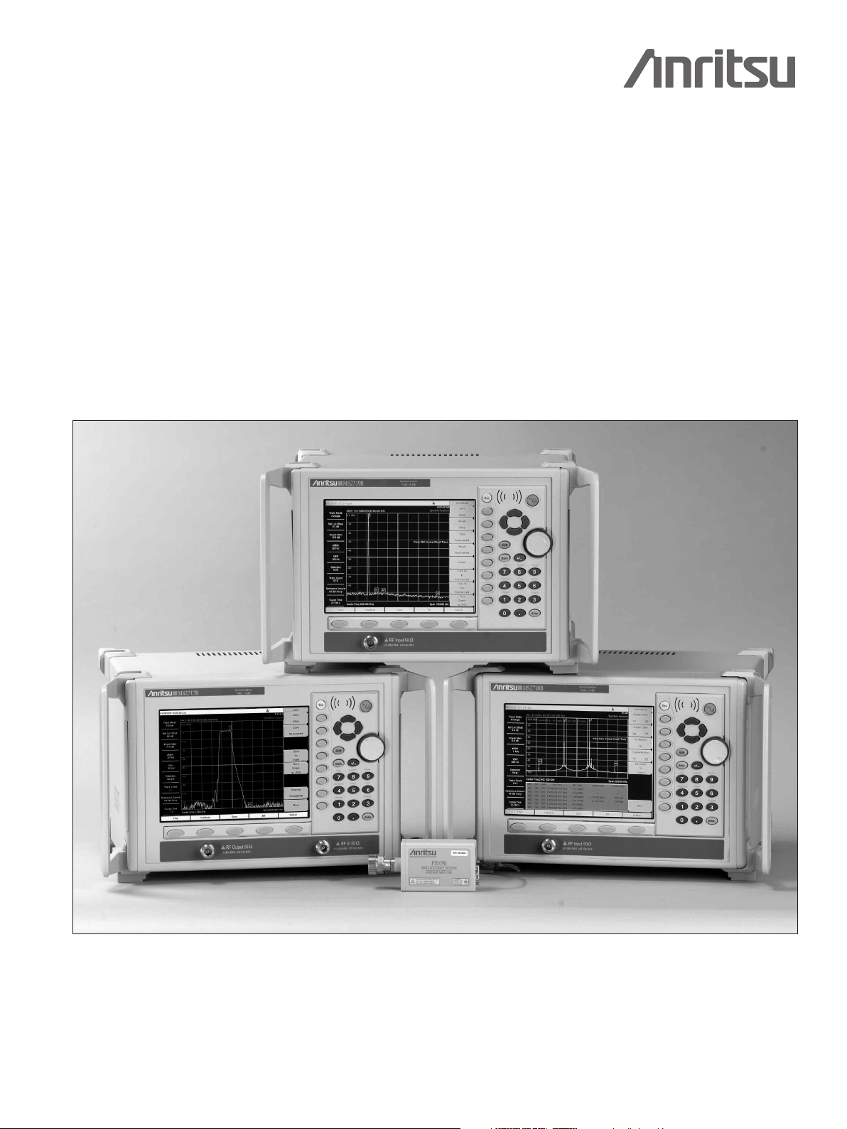
The MS2717B with Tracking Generator, MS2718B, MS2719B Economy Microwave Spectrum Analyzers, and PSN50 High Accuracy Power Sensor
Introduction
Engineers in R&D and manufacturing need advanced tools for spectrum analysis of wireless components in the critical
physical layer of modern communication systems. For best value and overall satisfaction, these general purpose tools
must deliver performance, capabilities, and the ability to lower the cost of testing. Anritsu’s new MS271xB Economy
Microwave Spectrum Analyzers offer superior performance and advanced capabilities. Take a closer look and we think you
will agree that the MS271xB family redefines the economy class by delivering superior spectrum analyzer performance
at a surprisingly affordable price.
Covering the 9 kHz to 7.1, 13 and 20 GHz ranges, the MS271xB family easily handles most RF and microwave spectrum
nalyzer needs. The hallmark of the MS271xB family is the phase noise performance: typical –110 dBc/Hz SSB phase
a
noise at 10 kHz offsets up to 7.1 GHz (MS2717B) which easily measures most wireless local oscillators and synthesizers.
The superior dynamic range of 100 dB means fast and precise testing of wireless components that require exceptional
linearity. The wide 10 MHz demodulation bandwidth supports optional W-CDMA/HSDPA, W-CDMA, and WiMAX
measurements. Best of all, the MS271xB family is ergonomically designed so controls are easy-to-learn and easy-to-use
for improving productivity in manufacturing, R&D, and general purpose testing.
Standard Measurements
• ACPR: Measures power levels in the channels
immediately above and below the center channel.
• Occupied Bandwidth: Measures 99% to 1% power
channel of a spectrum.
•
Channel Power: Measures the total power in a
specified bandwidth.
C/I: Measures carrier to interference ratio.
•
Optional Capabilities
• Tracking Generator option (MS2717B only)
• High Accuracy Power Meter Option
• Rack Mount Chassis:
Conveniently place MS271XB in 19 inch racks.
W-CDMA/HSDPA Measurements:
MS271xB family offers superior dynamic range for linear measurements of next
generation wireless components.
Typical Performance of the MS271xB family
• 9 kHz to 7.1, 13 and 20 GHz
• Standard Built-in Preamplifier
• Dynamic Range of 100 dB
• Third Order Intercept of +12 dBm
• DANL (No Preamp) of –126 dBm (RBW = 10 Hz)
• DANL (With Preamp) of –150 dBm (RBW = 10 Hz)
Phase Noise (800 MHz) of –1
•
at 10 kHz Of
• Amplitude Accuracy of ±1.0 dB to 20 GHz
• Sweep Speed of 200 ms in 10 MHz Span
(RBW = 30 kHz, VBW = 10 kHz)
• Demodulation Bandwidth of 10 MHz
• Residual
• Residual EVM of 1.75%
rue RMS Detection
T
•
• 65 dB Attenuation Range, 5 dB Steps
• 20 Watt (+43 dBm) Input Protection
fset
ACLR of –60 dB
14 dBc/Hz
•
Analyze the signal strength and mask.
• W-CDMA/HSDPA Demodulation:
Evaluate transmitter modulation performance using
Code Domain Power (CDP).
• WiMAX Measurements and Demodulation
(MS2717B only): Support fixed WiMAX testing and
verification.
ools
e T
Master Softw
• Anritsu Master Softwar
Powerful data management and pass/fail setup tool
indows
(W
al
Gener
• Easy-to-Learn Operation
• 8.4 inch Color TFT Display (SVGA)
• Eight Built-in Languages (plus T
• 256 MB Storage for 4,000 Traces and 4,000 Setups
• Six Markers, Nine Marker Modes
• Built-in AM/FM/SSB Demodulator
• Output Displays in JPEG Formats
• Connectivity: Ethernet, USB 2.0, Compact Flash
USB 2.0 Host connector for PSN50 High Accuracy
•
Power Meter and USB Flash Drives
• Remote Programming: Ethernet Only
• Compact Size and Weight: 5.6 kg (12 lbs)
• Operational –10ºC to 55ºC, Humidity < 85%
• 1 Year Standard Warranty
ar
®
2000/XP
ools:
e T
compatible).
wo Custom)
2
Specifications
Frequency
requency Range:
F
MS2717B: 9 kHz to 7.1 GHz
MS2718B: 9 kHz to 13.0 GHz
MS2719B: 9 kHz to 20.0 GHz
Preamplifier:
MS2717B: 100 kHz to 7.1 GHz
MS2718B and MS2719B: 100 kHz to 4.0 GHz
Frequency Span:
10 Hz to full frequency range, plus 0 Hz (zero span)
Tuning Resolution: 1 Hz
Dynamic Range
Using the popular dynamic range definition of 2/3
(TOI – DANL), the following specifications show the
excellent dynamic range that is available when using the
indicated tone spacing for TOI and RBW of 1 Hz.
um Dynamic Range using 2/3 (TOI-DANL),
Minim
–20 dBm tones, 100 kHz spacing, RBW = 1 Hz,
0 dB attenuation, Preamp = OFF
MS2717B: 600 MHz 95 dB, 3.5 GHz 96 dB
MS2718B and MS2719B: 2.4 GHz 101 dB
Typical Dynamic Range using 2/3 (TOI-DANL)
Typical Dynamic Range
(–20 dBm tones, 100 kHz spacing,
RBW = 1 Hz, 0 dB attenuation, Preamp = OFF)
Frequency MS2717B MS2718B MS2719B
10 MHz to 1.0 GHz 98 98 98
>1.0 GHz to 2.2 GHz 97 100 100
>2.2 GHz to 2.8 GHz 96 101 101
>2.8 GHz to 3.0 GHz 99 101 101
>3.0 GHz to 4.0 GHz 101 101 101
>4.0 GHz to 7.1 GHz 95 100 100
>7.1 GHz to 10 GHz N/A 100 100
>10 GHz to 13 GHz N/A 100 100
>13 GHz to 20 GHz N/A N/A 100
Displayed Average Noise Level (DANL)
sing 1 Hz RBW the following tables show maximum
U
DANL performance (not including discrete spurious).
eference level is –20 dBm for preamplifier off and –50
R
dBm for preamplifier on; RMS detection is used and
input attenuation is set to 0 dB.
Maximum Displayed Average Noise Level (DANL)
Maximum DANL (RBW = 1 Hz)
S2717B MS2718B MS2719B
M
requency
F
0 MHz to
1
.0 GHz
1
1.0 GHz
>
to 2.2 GHz
2.2 GHz
>
o 2.8 GHz
t
>2.8 GHz
to 3.0 GHz
>3.0 GHz
o 4.0 GHz
t
>4.0 GHz
7.1 GHz
to
7.1 GHz
>
o 10 GHz
t
>10 GHz
o 13 GHz
t
>13 GHz
to 20 GHz
Preamp
O
137 dBm –161 dBm –139 dBm –159 dBm –139 dBm –159 dBm
–
–133 dBm –159 dBm –139 dBm –156 dBm –139 dBm –156 dBm
126 dBm –153 dBm –139 dBm –156 dBm –139 dBm –156 dBm
–
–136 dBm –159 dBm –139 dBm –156 dBm –139 dBm –156 dBm
136 dBm –159 dBm –139 dBm –154 dBm –139 dBm –154 dBm
–
–127 dBm –154 dBm –136 dBm N/A –136 N/A
Noise Figur
The following table shows the calculated noise figure
from DANL measurements for 0 dB attenuation at 23ºC
with preamplifier on.
Equivalent Noise Figure, 23º C
Frequency MS2717B MS2718B MS2719B
10 MHz to 1.0 GHz 11 dB 15 dB 15 dB
>1.0 GHz to 2.2 GHz 14 dB 18 dB 18 dB
>2.2 GHz to 2.8 GHz 18 dB 18 dB 18 dB
>2.8 GHz to 3.0 GHz 14 dB 18 dB 18 dB
>3.0 GHz to 4.0 GHz 14 dB 20 dB 20 dB
>4.0 GHz to 7.1 GHz 16 dB 38 dB
>7.1 GHz to 10 GHz N/A 38 dB
>10 GHz to 13 GHz N/A 44 dB
>13 GHz to 20 GHz N/A N/A 38 dB
1
Preamplifier is limited to 4 GHz; equivalent noise figure values for
Preamp = Off –174 dBm/Hz (i.e., 1 Hz bandwidth at 23°C), 10 log (BW2/BW1)
Preamp
FF
/A N/A –136 dBm N/A –136 N/A
N
/A N/A –130 dBm N/A –130 N/A
N
N/A N/A N/A N/A –136 N/A
Preamp
N
O
O
Preamp
FF
Preamp
N
O
O
Preamp
FF
O
e
Equivalent Noise Figure, 23ºC, Preamp = On
1
1
1
38 dB
38 dB
44 dB
1
1
1
1
N
3
Third Order Intercept (TOI)
sing two –20 dBm tones separated by 100 kHz, the
U
following tables show the minimum and TOI performance.
eference level is set to –20 dBm, input attenuation is set
R
to 0 dB, and the preamplifier is off.
MS271xB Third Order Intercept for popular wireless
frequencies
Minimum Third Order Intercept (TOI), –20 dBm tones,
100 kHz spacing, RBW = 1 Hz, 0 dB attenuation,
Preamp = OFF
MS2717B: 600 MHz +7 dBm, 3.5 GHz +9 dBm
MS2718B and MS2719B: 2.4 GHz 12 dBm
Typical Third Order Intercept (TOI)
Typical TOI (–20 dBm tones, 100 kHz spacing, 0 dB attenuation)
requency MS2717B MS2718B MS2719B
F
50 MHz to 300 MHz >8 >6 >6
300 MHz to 500 MHz >10 >6 >6
>
>500 MHz to 2.0 GHz >10 >8 >8
>2.0 GHz to 2.2 GHz >10 >10 >10
2.2 GHz to 2.8 GHz >15 >10 >10
>
2.8 GHz to 3.0 GHz >10 >10 >10
>
>3.0 GHz to 4.0 GHz >13 >10 >10
>4.0 GHz to 7.1 GHz >13 >12 >12
>7.1 GHz to 10 GHz N/A >12 >12
>10 GHz to 1.3 GHz N/A >12 >12
>13 GHz to 20 GHz N/A N/A >12
Second Harmonic Distortion
(0 dB input attenuation, –30 dBm input):
Frequency Range Second Harmonic
0 MHz to 750 MHz
5
>750 MHz to 1.05 GHz –40 dBc
1.05 to 1.4 GHz
>
>1.4 to 2 GHz –70 dBc
>2 GHz –80 dBc
50 dBc
–
50 dBc
–
Amplitude
Maximum Continuous Input: (≥10 dB attenuation),
+30 dBm Input Damage Level*:
ttenuation Setting
A
10 dB >+43 dBm
≥
<10 dB >+23 dBm ± 50 Vdc
*Input protection relay opens at >30 dBm with ≥10 dB input attenuation and at approximately
10 to 23 dBm with <10 dB attenuation. ESD Damage Level: >10 kV with ≥10 dB attenuation.
nput Damage Level*
I
50 Vdc
±
Amplitude Accuracy
Amplitude accuracy at 50 MHz: ± 0.7 dB (20°C to 30°C)
MS2717B (30 minute warmup)
Overall Amplitude Accuracy: (-10°C to 55°C)
Power levels:
≥–50 dBm, ≤35 dB input attenuation
kHz to ≤10 MHz
9
>10 MHz to 4 GHz ±1.25 dB
>4 to 7.1 GHz ±1.75 dB
40 to 55 dB input attenuation
9 kHz to ≤10 MHz ±1.5 dB
>10 MHz to 4 GHz ±1.75 dB
>4 to 6.5 GHz ±1.75 dB
>6.5 to 7.1 GHz ±2 dB
1.5 dB
±
MS2717B family typical Third Order Intercept for popular wireless frequencies.
Typical TOI
The following table shows the excellent TOI that is typically
available for popular wireless frequencies and tone spacings.
ypical TOI
Frequency
900 MHz 13 dBm 18 dBm
1900 MHz 17 dBm 24 dBm
2300 MHz 20 dBm 27 dBm
2500 MHz 20 dBm 29 dBm
2700 MHz 20 dBm 30 dBm
3500 MHz 16 dBm 20 dBm
5800 MHz 13 dBm 23 dBm
T
(Offset = 100 kHz)
ypical TOI
T
(Offset = 15 MHz)
60 to 65 dB input attenuation
9 kHz to ≤10 MHz ±1.5 dB
>10 MHz to 6.5 GHz ±1.75 dB
>6.5 to 7.1 GHz ±3 dB
Preamplifier on, 0 or 10 dB input attenuation
9 kHz to 4 GHz ±1.5 dB
>4 to 7.1 GHz ±1.75 dB
MS2718B and MS2719B (30 minute warmup)
Overall Amplitude Accuracy: (20°C to 30°C) ±1.3 dB
Frequency Flatness: >4 GHz add ±1.5 dB
4

Amplitude Settings
ttenuator Range:0to 65 dB
A
Attenuator Resolution: 5 dB steps
easurement Range:DANL to +30 dBm
M
Display Range: 1 to 15 dB/div in 1 dB steps
en divisions displayed
T
Time Base Stability
requency Reference:
F
Condition Specification
5ºC ± 25ºC, Aging < ±1 ppm/10 yrs
2
25ºC ± 25ºC, < ±0.3 x 10
pan Accuracy:Same as frequency reference accuracy
S
–
6
/yr or 0.3 ppm/yr + aging
Amplitude Units
Modes Units
Log Scale dBm, dBV, dBmv, dBµV
Linear Scale nV, µV, mV, V, kV, nW, µW, mW, W, kW
Resolution and Video Bandwidth (RBW,VBW)
Resolution Bandwidth:
(–3 dB) 1 Hz to 3 MHz in 1-3 sequence ±10%,
200 Hz, 9 kHz, 120 kHz when quasi-peak detector
selected
Demodulation Bandwidth: 10 MHz
ideo Bandwidth:
V
(–3 dB) 1 Hz to 3 MHz in 1-3 sequence
SSB Phase Noise:
Sweep Times
Sweep Time:
ero span: 10 us to 600s
Z
Spans >0 Hz: Minimum 200 ms, automatically
optimized. Can be manually increased
Sweep Time Accuracy: ±2% in zero span
Sweep Trigger: Free run, Single, Video, External
Sweep Span:
Full span, zero span, and span up/span down
Typical Sweep Time (sample detection)
pan
S
0 GHz (MS2719B)
2
3 GHz (MS2718B)
1
6 GHz 3 MHz 1 MHz 400 ms
00 MHz
2
0 MHz
1
.2 kHz
2
100 Hz 1 Hz 3 Hz 5 sec
R
3
3
00 kHz
3
0 kHz
3
1
BW
MHz
MHz
0 Hz
V
1
1
00 kHz
1
0 kHz
1
3
BW
MHz
MHz
Hz
ypical Sweep Time
T
00 ms
9
00 ms
9
00 ms
2
00 ms
2
49 ms
1
MS2717B family typical Phase Noise at 800 MHz.
Frequency Range
Model(s)
Offset From Carrier
10, 20 and 30 kHz –100 (110) dBc/Hz –95 (102) dBc/Hz –91 (99) dBc/Hz
100 kHz –102 (112) dBc/Hz –97 (104) dBc/Hz –93 (101) dBc/Hz
1 MHz –100 (1
10 MHz –100 (1
9 kHz to 7.1 GHz
MS2717B
SSB Phase Noise
(typical)
10) dBc/Hz
10) dBc/Hz
9 kHz to 13 GHz
MS2718B/19B
SSB Phase Noise
(typical)
12) dBc/Hz
–105 (1
–120 (126) dBc/Hz –1
>13 GHz to 20 GHz
MS2719B
SSB Phase Noise
(typical)
–102 (109) dBc/Hz
16 (123) dBc/Hz
5

Input-Related Spurious:
–30 dBm input, 0 dB input attenuation, Span <1.7 GHz)
(
–70 dBc typical –60 dBc max
1
2
MS2717B Residual Spurious:
Preamplifier on, RF input terminated, 0 dB input
(
attenuation)
–100 dBm max
(Preamplifier off, RF input terminated, 0 dB input
attenuation)
–90 dBm max*, 100 kHz to <3200 MHz
–84 dBm max*, 3200 to 7100 MHz
*Exceptions:
Frequency Max Spur Level (Typical)
250, 300, and 350 MHz –85 dBm
4010 MHz
~
5084 MHz
~
~5894 MHz –75 dBm (–87 dBm)
7028 MHz
~
80 dBm (–90 dBm)
–
70 dBm (–83 dBm)
–
80 dBm (–92 dBm)
–
MS2718/MS2719B Residual Spurious:
(Preampifier on, RF input terminated, 0 dB input
attenuation)
–100 dBm max
(Preamplifier off, RF input terminated, 0 dB input
attenuation)
–90 dBm max
–85 dBm max, >13 GHz
1
Discrete spurious signals are not included in the measurement of DANL as they are
covered by the residual spurious specification.
2
MS2718B, MS2719B except input frequency 3275 MHz, –50 dBc max.
Options Specifications
D
emodulation Hardware (Option 9)
Needed to run any of the demodulation options
PSN50 High Accuracy Power Meter Functionality
(Option 19)
PSN50 Sensor:
Measurement Range: –30 dBm to +20 dBm
Frequency Range: 50 MHz to 6 GHz
Input Connector: Type N, male, 50Ω
Max Input Without Damage: +33 dBm, ±25 VDC
Input Return Loss:
50 MHz to 2 GHz: ≥26 dB
2 GHz to 6 GHz: ≥20 dB
PSN50 Accuracy:
Total RSS Measurement Uncertainty (0ºC to 50ºC):
±0.16 dB
Noise: 20 nW max
Zero Set: 20 nW
Zero Drift: 10 nW max
Sensor Linearity: ±0.13 dB max
Instrumentation Accuracy: 0.00 dB
Sensor Cal Factor Uncertainty: ±0.06 dB
Temperature Compensation: ±0.06 dB max
Continuous Digital Modulation Uncertainty:
±0.06 dB (+17 to +20 dBm)
PSN50 System:
Measurement Resolution: 0.01 dB
Offset Range: ±60 dB
1
Excludes mismatch errors
2
After 30 min warm-up
Tracking Generator, Option 20 (MS2717B only)
Frequency Range: 100 kHz to 7.1 GHz
Frequency Resolution: 1 Hz
Frequency Accuracy (25ºC ±25ºC):
Same as spectrum analyzer
Output P
Step Size: 0.1 dB nominal
Level Accuracy (15ºC to 35ºC):
±1.5 dB max, 450 kHz to 7.1 GHz,
excluding SWR effects
Zero Span Behavior: CW Output
Output Connector:T
Damage Levels: +23 dBm, ±50V DC
Phase Noise: –100 dBm/Hz max at 10 kHz offset.
(1 GHz, 0 dBm CW output)
1
:
er
w
o
0 dBm to –40 dBm
2
ype N female, 50
Ω
6

W-CDMA/HSDPA Analysis (Options 44, 45, 65)
he following table shows the capability of Options 44
T
and 45 to analyze W-CDMA/HSDPA modulation quality.
ption 45 requires the demodulation hardware, Option 9.
O
W-CDMA/HSDPA Option Comparison Table
-CDMA Demodulator
W
ption 45, and
-CDMA/HSDPA
W
Measurements
and Spectrum
B
hannel Spectrum
C
arrier Frequency
C
requency Error
F
hannel Power
C
ccupied Bandwidth
O
eak to Average Power
P
Noise Floor
ACLR
pectral Emission Mask
S
-CPICH
P
Abs Power
EVM
Symbol EVM
Carrier Feed Through
Peak CD Error
CPICH
P-CCPCH Power
S-CCPCH Power
PICH
P-SCH Power
S-SCH Power
Pass/Fail Mode
-CDMA/HSDPA RF
W
Measurements
ption 44
O
3
3
3 3
3 3
3 3
3
3
3
3
3
3 3
O
-CDMA/HSDPA
W
Demodulator Option 65
Option 65 includes Option
(
5 capability)
4
3
3
3
3
3
3
3
3
3
3
3
Option 44 Example
he superior performance of the MS271XB family
T
ensures precise measurements of Adjacent Channel
eakage Ratio (ACLR) when coupled with a vector signal
L
generator.
MS271xB family has optional Adjacent Channel Leakage Ratio (ACLR) measurements when connected to Anritsu’s MG3700A Vector Signal Generator.
W-CDMA/HSDP
The following measurement performance is available for
analyzing the modulation quality of selected transmitters.
Measurement
RF Channel Power
15°C to 30°C
Occupied Bandwidth ±100 kHz
Residual ACLR
(5 MHz Offset)
ACLR Accuracy: 5 MHz
Of
fset ACLR ≥–45 dB
Residual ACLR
(10 MHz Offset)
ACLR
Accuracy:
10 MHz Offset
ACLR ≥–50 dB
Frequency Error ±10 Hz +
A RF Measurements (Option 44)
824-894 MHz,
1710-2170 MHz
±1.25 dB max, ±0.7 dB typical
1
±0.8 dB ±1.0 dB
–59 dB typ –57 dB typ
±0.8 dB ±1.0 dB
–54 dB typ
ime Base Error
T
, 99% confidence level
2300-2700 MHz
7

W-CDMA Demodulation (Option 45)
he following measurement performance is available for
T
analyzing the modulation quality of selected transmitters
requires Option 9).
(
24-894 MHz,
easurement
M
VM Accuracy
E
3GPP Test Model
VM ≤25%
E
EVM Accuracy 3GPP
est Model 5
T
VM ≤20%
E
Residual EVM1 2.5% typical
Code Domain Power:
est Model 1,
T
16, 32, 64, DCPH
hannel Power >–25 dB
C
ode Domain Power:
C
est Model 2,
T
3, 16, 32, DCPH
hannel Power >–25 dB
C
PICH (dBm)
C
crambling Code
S
8
1710-2170 MHz
±2.5% ±2.5%
2.5%
±
0.5 dB
±
±0.5 dB
0.8 dB typ
±
seconds
3
300-2700 MHz
2
2.5%
±
Option 45 Example
se any of the five 3GPP models covering all eleven test
U
scenarios (TS 25.141) for easy pass/fail testing.
S271xB family has optional PA
M
to 3GPP test models.
SS/FAIL summary screens to easily verify compliance
Fixed WiMAX RF Measurements
(Option 46, MS2717B onl
Channel Power Accuracy:
±1 dB typical for +20 dBm to –50 dBm (±1.5 dB max)
y)
Fixed WiMAX Demodulator
(Option 47, MS2717B only, Requires Option 9)
Residual EVM (rms):
3% for +20 dBm to –50 dBm (3.5% max.)
Frequency Error:
±10 Hz + time base error, 99% confidence level
8

General
arkers and Limit Lines
M
6 Markers, 9 Modes: Normal, Delta, Marker to Peak, Marker to Center, Marker to
Reference Level, Next Peak Left, Next Peak Right, All Markers Off, Noise Marker,
Frequency Counter Marker (1 Hz resolution), Markers Tracking or Fixed, Marker 1
reference for all deltas.
Multiple Marker: Display up to six markers on screen. Each marker includes a delta
marker, effectively allowing up to 12 markers on screen.
M
arker Table:Display a table of up to six marker frequency and amplitude values plus
delta marker frequency offset and amplitude.
Limit Lines: Display upper and lower fixed and segmented limit lines, where each upper
and lower limit can be made up of between one and 40 segments.
Miscellaneous
Detection: Peak, Negative, Sample, RMS, Quasi-peak
Displayed Traces: Three Traces with trace overlay. Trace A is always the live data;
T
races B and C can be either stored data or traces which have been mathematically
manipulated. Also Trace C can show max hold or min hold.
Memory: Trace and Setup storage is limited only by the capacity of the installed
Compact Flash card or USB Flash drive. For a 256 MB card, storage is greater than
13000 spectrum analyzer traces and over 10000 setups.
Languages: Built-in English, Spanish, Italian, French, German, Japanese, Korean, and
Chinese. The instrument also has the capability to have customized languages and
soft key definitions installed from Master Software Tools.
Display
Display: Bright color transmissive LCD, Full SVGA, 8.4 inches
Connectivity
For convenient connection to PCs and networks, the MS271xB family offers an RJ45
connector for Ethernet 10/100 Base T connections. Alternatively, a 5-pin Mini-B USB 2.0
(full speed) connection is provided for connection to a PC. USB 2.0 Host connector used
with PSN50 High Accuracy Power Meter and USB Flash Drives
Interfaces
RF Input Connector: Type N female
RF Input VSWR (>10 dB attenuation):
MS2717B, MS2718B; 2.0:1 maximum, 1.5:1 typical
M
S2719B; 2.0:1 maximum, 1.5:1 typical <13 GHz, 2:1 typical 13 to 20 GHz
External Reference Input Connector: BNC female
External Reference Frequencies:
1, 1.2288, 1.544, 2.4576, 4.8, 4.9152, 5, 9.8304, 10, 13 and 19.6608 MHz
at –10 to +10 dBm
E
xternal Trigger Connector:BNC female, TTL Signal
External Headphone Jack
Speaker
Remote Programming
SCPI available via Ethernet
ower Requirements
P
90 to 250 VAC, 47-63 Hz, 35 VA maximum
Size and Weight
Size with handles: 372W x 242H x 339D mm (14.7W x 9.6H x 13.4D in)
S
ize with rack mount:483W x 242H x 339D mm (19W x 9.6H x 13.4D in)
Weight: 5.6 kg (12 lbs)
Environmental
MIL-PRF-28800F class 2
Operating: –10ºC to 55ºC, humidity 85% or less
Storage: –51ºC to 71ºC
Altitude: 4600 meters, operating and non-operating
Safety
Conforms to EN 61010-1 for Class 1 portable equipment
Electromagnetic Compatibility Meets European Community requirements for CE marking.
Light weight: 5.6 kg (12 lbs)
Small footprint: 372W x 242H x 339D mm
Use higher capacity compact flash cards
to increase storage capacity for traces
and setups.
(14.7W x 9.6H x 13.4D in)
MS271xB Rear Panel
Rear-panel female BNC connectors
for an external reference source and
external trigger.
Simple PC and network hookups with
five-pin Mini-B USB 2.0 port and an
Ethernet 10/100 Base-T local area network (LAN) RJ45 connector.
USB 2.0 Host connector for PSN50
High Accuracy Power Meter and USB
Flash Drives.
Popular 2.5 mm 3-wire cellular headset
connector for listening to demodulated
signals.
9

Ordering Information
All models include standard 1 year warranty plus
Certificate of Calibration and Conformance
MS2717B Economy Microwave Spectrum Analyzer
9 kHz to 7.1 GHz, including preamplifier
MS2718B Economy Microwave Spectrum Analyzer
kHz to 13.0 GHz, including preamplifier
9
S2719B Economy Microwave Spectrum Analyzer
M
9 kHz to 20.0 GHz, including preamplifier
Optional Rack Mount Kit
Options
S271xB-001 Rack Mount (No Slides)
M
MS271xB-009 Modulation Demodulation Hardware
MS271xB-019 High Accuracy Power Meter Functionality
MS2717B-020 Tracking Generator (MS2717B only)
MS271xB-044 W-CDMA/HSDPA RF Measurements
MS271xB-045 W-CDMA Demodulator(Requires Option 009)
MS2717B-046 Fixed WiMAX RF Measurements (MS2717B only)
MS2717B-047
MS271xB-065 W-CDMA/HSDPA Demodulator (requires Opt. 009,
MS271xB/98 Z540/ISO Guide 25 Calibration
MS271xB/99 Premium Calibration
Fixed WiMAX Demodulation (MS2717B only,
requires Opt. 009)
includes option 45 capability)
MS271xB-001 Rack Mount (No Slides)
Optional Transit Case
760-240-R MS271xB Transit Case
Standar
10580-00181 Anritsu User
2300-498 CD ROM containing Master Software Tools
3-2000-1498 USB A-mini B cable
2000-1371 RJ45 Ethernet Cable
3-2000-1500
2000-1501 256 MB USB Flash Drive
1091-27 Type-N male to SMA Female Adapter
1091-172 Type-N male to BNC Female Adapter
d Accessories
’s Guide, Models MS271xB
256 MB Compact Flash
10

Optional Accessories
PSN50 High Accuracy Sensor
3-2000-1500 256 MB Compact Flash
2000-1501 256 MB USB Flash Drive
2000-1209 Cross-over Ethernet Cable
2N50A-30 30 dB, 50 watt, Bi-directional, DC to 18 GHz,
4
N(m) to N(f) Attenuator
34NN50A Precision Adapter, DC to 18 GHz, 50
34NFNF50C Precision Adapter, DC to 18 GHz, 50
15NNF50-1.5B Test port cable, armored, 1.5 meter, N(m) to N(f) 18 GHz
15NN50-1.5C Test port cable armored, 1.5 meter, N(m) to N(m), 6 GHz
15NN50-3.0C Test port cable armored, 3.0 meter, N(m) to N(m), 6 GHz
15NN50-5.0C Test port cable armored, 5.0 meter, N(m) to N(m), 6 GHz
15NNF50-1.5C Test port cable armored, 1.5 meter, N(m) to N(f), 6 GHz
15NNF50-3.5C Test port cable armored, 3.0 meter, N(m) to N(f), 6 GHz
15NNF50-5.0C Test port cable armored, 5.0 meter, N(m) to N(f), 6 GHz
Ω, N(m) to N(m)
Ω, N(f) to N(f)
5ND50-1.5C Test port cable armored, 1.5 meter,
1
N(m) to 7/16 DIN(m), 6.0 GHz
15NDF50-1.5C Test port cable armored, 1.5 meter,
N(m) to 7/16 DIN(f), 6.0 GHz
10-90 Adapter, 7/16 DIN (f) to N(m), DC to 7.5 GHz, 50
5
10-91 Adapter, 7/16 DIN (f)-N(f), DC to 7.5 GHz, 50
5
10-92 Adapter, 7/16 DIN(m)–N(m), DC to 7.5 GHz, 50
5
10-93 Adapter, 7/16 DIN(m)-N(f), DC to 7.5 GHz, 50
5
10-96 Adapter 7/16 DIN (m) to 7/16 DIN(m),
5
DC to 7.5 GHz, 50Ω
510-97 Adapter 7/16 DIN(f) to 7/16 DIN(f), 7.5 GHz
Ω
Ω
Literature
10580-00181 Anritsu User’s Guide, Models MS271xB
10580-00182 Anritsu Programming Manual, Models MS271xB
11410-00418 MS271xB Family Brochure
Ω
Ω
11

ANRITSU Corporation
5-1-1 Onna, Atsugi-shi, Kanagawa, 243-8555 Japan
Phone: +81-46-223-1111
F
ax: +81-46-296-1264
- U.S.A.
ANRITSU Company
1155 East Collins Boulevard, Suite 100,
Richardson, Texas 75081
Toll Free: 1-800-ANRITSU (267-4878)
Phone: +1-972-644-1777
Fax: +1-972-671-1877
- Canada
ANRITSU Electronics Ltd.
700 Silver Seven Road, Suite 120, Kanata,
Ontario K2V 1C3, Canada
Phone: +1-613-591-2003
Fax: +1-613-591-1006
- Brazil
ANRITSU Electrônica Ltda.
Praca Amadeu Amaral, 27-1 andar
01327-010 - Paraiso, São Paulo, Brazil
Phone: +55-11-3283-2511
Fax: +55-11-3886940
- U.K.
ANRITSU EMEA Ltd.
200 Capability Green, Luton, Bedfordshire LU1 3LU, U.K.
Phone: +44-1582-433280
Fax: +44-1582-731303
- France
ANRITSU S.A.
9, Avenue du Québec Z.A. de Courtaboeuf
91951 Les Ulis Cedex, France
Phone: +33-1-60-92-15-50
Fax: +33-1-64-46-10-65
- Germany
ANRITSU GmbH
Nemetschek Haus, Konrad-Zuse-Platz 1
81829 München, Germany
Phone: +49 (0) 89 442308-0
Fax: +49 (0) 89 442308-55
- Italy
ANRITSU S.p.A.
Via Elio Vittorini, 129, 00144 Roma, Italy
P
hone: +39-06-509-9711
Fax: +39-06-502-2425
- Sweden
ANRITSU AB
Borgafjordsgatan 13, 164 40 Kista, Sweden
Phone: +46-8-534-707-00
Fax: +46-8-534-707-30
- Finland
ANRITSU AB
Teknobulevardi 3-5, FI-01530 V
Phone: +358-20-741-8100
Fax: +358-20-741-81
antaa, Finland
11
- Denmark
ANRITSU A/S
Kirkebjerg Allé 90 DK-2605 Brondby, Denmark
Phone: +45-72112200
Fax: +45-72112210
- Spain
Anritsu EMEA Ltd.
Oficina de Representación en España
eganova
Edificio V
vda de la V
A
28108
Phone: +34-914905761
Fax: +34-914905762
ega, nº 1 (edf 8, pl1, of 8)
ALCOBENDAS - Madrid, Spain
- United Arab Emirates
ANRITSU EMEA
Ltd.
Dubai Liaison Office
P O Box 500413 - Dubai Internet City
Al Thuraya Building, Tower 1, Suit 701, 7th Floor
Dubai, United Arab Emirates
Phone: +971-4-3670352
Fax: +971-4-3688460
- Singapore
ANRITSU Pte. Ltd.
10, Hoe Chiang Road #07-01/02, Keppel Towers,
Singapore 089315
Phone: +65-6282-2400
Fax: +65-6282-2533
- P. R. China (Hong Kong)
ANRITSU Company Ltd.
U
nits 4 & 5, 28th Floor
N
o. 1 Science Museum Road, Tsim Sha Tsui East,
Kowloon, Hong Kong, P.R. China
Phone: +852-2301-4980
Fax: +852-2301-3545
, Greenfield To
wer, Concordia Plaza,
- P. R. China (Beijing)
ANRITSU Company Ltd.
Beijing Representative Office
Room 1515, Beijing Fortune Building,
No. 5 , Dong-San-Huan Bei Road,
Chao-Yang District, Beijing 100004, P.R. China
Phone: +86-10-6590-9230
Fax: +82-10-6590-9235
- Korea
ANRITSU Corporation, Ltd.
eoksam-Dong,
8F Hyunjuk Bldg. 832-41,
Kangnam-ku, Seoul, 135-080, Korea
Phone: +82-2-553-6603
Fax: +82-2-553-6604
Y
- Australia
ANRITSU Pty Ltd.
Unit 21/270 Ferntree Gully Road, Notting Hill
ictoria, 3168, Australia
V
Phone: +61-3-9558-8177
Fax: +61-3-9558-8255
- Taiwan
ANRITSU Company Inc.
, No. 316, Sec. 1, Neihu Rd.,
7F
Phone: +886-2-8751-1816
Fax: +886-2-8751-1817
Taipei 114, Taiwan
- India
ANRITSU Pte. Ltd.
India Liaison Office
Unit No.S-3, Second Floor, Esteem Red Cross Bhavan,
No.26, Race Course Road, Bangalore 560 001 India
Phone: +91-80-32944707
Fax: +91-80-22356648
®Anritsu All trademarks are registered trademarks of
their respective companies. Data subject to change
notice. For the most recent specifications visit:
without
.us.anritsu.com
www
Technical Data Sheet No. 11410-00417, Rev. A Printed in United States 2007-03
 Loading...