

Page 1
MODEL
MN4790A TEST SET FOR THE
ME7842B
TOWER MOUNTED AMPLIFIER TEST SYSTEM
MAINTENANCE MANUAL
490 JARVIS DRIVE l MORGAN HILL, CA 95037-2809
P/N: 10410-00245
REVISION: A
PRINTED: MARCH 2003
COPYRIGHT 2003 ANRITSU CO.
Page 2

WARRANTY
The Anritsu product(s) listed on the title page is (are) warranted against defects in materials and
workmanship for three years from the date of shipment.
Anritsu’s obligation covers repairing or replacing products which prove to be defective during the
warranty period. Buyersshall prepaytransportation chargesfor equipment returned to Anritsu for
warranty repairs. Obligation is limited to the original purchaser. Anritsu is not liable for
consequential damages.
LIMITATION OF WARRANTY
The foregoing warranty does not apply to Anritsu connectors that have failed due to normal wear.
Also,the warranty does not apply to defects resulting from improper or inadequate maintenance by
the Buyer, unauthorized modification or misuse, or operation outside of the environmental
specifications of the product.No otherwarranty isexpressed or implied, andthe remedies provided
herein are the Buyer’s sole and exclusive remedies.
TRADEMARK ACKNOWLEDGEMENTS
Scorpion and Scorpion Navigator are registered trademarks of Anritsu Company.
Windows is a registered trademark of Microsoft Corporation.
NOTICE
Anritsu Company has prepared this manual for use by Anritsu Company personnel and customers
as a guide for the proper installation, operation and maintenance of Anritsu Company equipment
and computer programs. The drawings, specifications, and information contained herein are the
property of Anritsu Company, and any unauthorized use or disclosure of these drawings,
specifications, and information is prohibited; they shall not be reproduced,copied, or used in whole
or in part as the basis for manufacture or sale of the equipment or software programs without the
prior written consent of Anritsu Company.
Page 3

Symbols used in manuals
Safety Symbols
To prevent the risk of personal injury or loss related to equipment
malfunction, ANRITSU Company uses the following symbols to indi
cate safety-related information. For your own safety, please read this
information carefully BEFORE operating the equipment.
-
DANGER
Indicates a very dangerous procedure that could result in serious in
jury or death if not performed properly.
WARNING Indicates a hazardous procedure that could result in serious injury or
death if not performed properly.
CAUTION Indicates a hazardous procedure or danger that could result in light-
to-severe injury, or loss related to equipment malfunction, if proper
precautions are not taken.
Safety Symbols Used on Equipment and in Manuals
Some or all of the following five symbols may or may not be used on all ANRITSU equipment. In addition,
there may be other labels attached to products that are not shown in the diagrams in this manual.
The following safety symbols are used inside or on the equipment near
operation locations to provide information about safety items and op
eration precautions. Ensure that you clearly understand the meanings
of the symbols and take the necessary precautions BEFORE operating
the equipment.
This symbol indicates a prohibited operation. The prohibited operation
is indicated symbolically in or near the barred circle.
-
-
This symbol indicates a compulsory safety precaution. The required
operation is indicated symbolically in or near the circle.
This symbol indicates warning or caution. The contents are indicated
symbolically in or near the triangle.
This symbol indicates a note. The contents are described in the box.
These symbols indicate that the marked part should be recycled.
MN4790A MM Safety-1
Page 4

For Safety
WARNING
Always refer to the operation manual when working near locations at
which the alert mark, shown on the left,is attached. If the operation, etc.,
is performed without heeding the advice in the operation manual, there is
a risk of personal injury. In addition, the equipment performance may be
reduced.
Repair
WARNING
Moreover, this alert mark is sometimes used with other marks and descrip
tions indicating other dangers.
WARNING
When supplying AC power to this equipment, connect the accessory 3-pin
power cord to a 3-pin grounded power outlet. If a grounded 3-pin outlet is
not available, use a conversion adapter and ground the green wire, or
connect the frame ground on the rear panelof the equipment to ground. If
power is supplied without grounding the equipment, there is a risk of receiving a severe or fatal electric shock.
WARNING
This equipment cannot be repaired by the operator. DO NOT attempt to re
move the equipment covers or to disassemble internal components. Only
qualified service technicians with a knowledge of electrical fire and shock
hazards should service this equipment. There are high-voltageparts in this
equipment presenting a risk of severe injury or fatal electric shock to un
trained personnel. In addition, there is a risk of damage to precision com
ponents.
-
-
-
-
WARNING
If this equipment is used in a manner not specified by the manufacturer,
the protection provided by the equipment may be impaired.
Safety-2 MN4790A MM
Page 5

Table of Contents
Chapter 1 General Information
1-1 SCOPE OF MANUAL .......................1-1
1-2 INTRODUCTION .........................1-1
1-3 IDENTIFICATION NUMBER ..................1-1
1-4 ONLINE MANUAL ........................1-1
1-5 TMATS SYSTEM OVERVIEW ..................1-2
1-6 HARDWARE DESCRIPTION...................1-2
1-7 SYSTEM DESCRIPTION .....................1-2
MS4623B VNMS ·······················1-2
MN4790A Test Set ······················1-3
1-8 RECOMMENDED TEST EQUIPMENT .............1-6
1-9 STATIC SENSITIVE
COMPONENT HANDLING PROCEDURES...........1-6
1-10 SERVICE CENTERS .......................1-8
Chapter 2 Replaceable Parts
2-1 INTRODUCTION .........................2-1
2-2 EXCHANGE ASSEMBLY PROGRAM ..............2-1
2-3 REPLACEABLE SUBASSEMBLIES AND PARTS .......2-2
2-4 PARTS ORDERING INFORMATION ..............2-2
Chapter 3 Performance Verification Procedure
3-1 INTRODUCTION .........................3-1
3-2 CONVENTIONS..........................3-1
3-3 PRELIMINARY ..........................3-1
MS4623B VNMS ·······················3-1
ME7842B TMATS ······················3-2
Required Equipment·····················3-2
Preliminary Setup ······················3-2
3-4 DIRECTIVITY AND TEST PORT MATCH............3-5
Test Procedure ························3-5
3-5 DYNAMIC RANGE........................3-11
Test Procedure ·······················3-11
MN4790A MM i
Page 6

3-6 IMD MEASUREMENT......................3-14
Test procedure ·······················3-14
Chapter 4 Troubleshooting
4-1 INTRODUCTION .........................4-1
4-2 OPERATIONAL CHECK .....................4-1
Required Equipment·····················4-1
4-3 INTERNAL SIGNAL PATH INSERTION LOSS CHECK....4-1
Test Setup ··························4-1
Test Procedure ························4-2
4-4 TEST CHANNEL STEP ATTENUATOR CHECK ........4-4
Test Setup ··························4-4
Test Procedure ························4-4
4-5 TROUBLESHOOTING ......................4-6
Test Set Fails to Power Up··················4-6
Line Source and Interface Checks··············4-6
Power Supply Voltage Check ················4-6
Chapter 5 Removal and Replacement Procedures
5-1 INTRODUCTION .........................5-1
5-2 EQUIPMENT REQUIRED ....................5-1
5-3 REMOVING THE COVERS....................5-1
Preliminary··························5-1
Procedure···························5-1
5-4 A1 GPIB PARALLEL INTERFACE PCB .............5-4
5-5 A2 COMBINER ..........................5-5
5-6 A3 STEP ATTENUATOR .....................5-6
5-7 A4 AND A5 BIAS TEES......................5-7
5-8 A6 POWER SUPPLY .......................5-8
5-9 A7 CONTROL PCB .......................5-10
5-10 FAN ASSEMBLY.........................5-11
5-11 SP3T AND SPDT SWITCHES..................5-12
ii MN4790A MM
Page 7

Appendix A Connector Maintenance Check Procedures
A-1 INTRODUCTION .........................A-1
A-2 PRECAUTIONS ..........................A-1
Pin Depth Problems ·····················A-1
Pin Depth Tolerance·····················A-2
Avoid Over Torquing Connectors ··············A-2
Teflon Tuning Washers ···················A-2
Avoid Mechanical Shock ··················A-2
Keep Connectors Clean ···················A-3
Visual Inspection ······················A-3
A-3 REPAIR AND MAINTENANCE .................A-3
Index
MN4790A MM iii/vi
Page 8

Page 9

Chapter 1 General Information
1-1 SCOPE OF MANUAL This manual provides general service and preventive maintenance
information for the Anritsu MN4790A test set for the ME7842B Tower
Mounted Amplifier Test System.It contains procedures for:
Testing the instrument for proper operation
q
Verifying measurement accuracy and traceability to National In
q
stitute of Standards and Technology (NIST)
-
Troubleshooting a failed instrument to the exchange subassem
q
bly level or to the subsystem requiring adjustment
Locating and replacing failed parts
q
Throughout this manual, the terms ME7842B and Tower Mounted
Amplifier Test System (or TMATS) will be used interchangeably to re-
fer to the entire ME7842B Tower Mounted Amplifier Test System;the
terms MS4623B, Vector Network Measurement System (or VNMS), and
Scorpion
Vector Network Measurement System; the terms MN4790A and test
set will be used interchangeably to refer to the model MN4790A test
set, unless otherwise noted.
®
will be used interchangeably to refer to the model MS4623B
1-2 INTRODUCTION This chapter provides a general description of the T owerMounted
Amplifier Test System’ sserial numbers ,frequency ranges, and related
manuals.It alsoincludes a service strategy,availableservice facilities ,
static-sensitive component handling precautions, and a list of recom
mended test equipment.
1-3 IDENTIFICATION
NUMBER
All Anritsu instruments are assigned a six-digit ID number, such as
“021001.”This number appears on a decal affixed to the rear panel.
Please use this identification number during any correspondence with
Anritsu Customer Service about this instrument.
-
-
1-4 ONLINE MANUAL This manual is available on CD ROM as an Adobe Acrobat™ (*.pdf)
file. The file can be viewed using Acrobat Reader™, a free program
that is also available on the CD ROM. This file is “linked” such that
the viewer can choose a topic to view from the displayed “bookmark”
list and “jump” to the manual page on which the topic resides.The text
can also be word-searched. A copy of this CD ROM can be ordered
from Anritsu.
MN4790A MM 1-1
Page 10

TMATS SYSTEM OVERVIEW GENERAL INFORMATION
1-5 TMATS SYSTEM
OVERVIEW
1-6 HARDWARE
DESCRIPTION
The Anritsu ME7842B Tower Mounted Amplifier Test System is in
tended for the measurement and real-time graphical displayof a tower
mounted amplifier in the frequency range from 10 MHz to 6 GHz of
the following parameters:
S-Parameters Including Hot S
q
K-Factor
q
Gain Compression and Phase Distortion
q
Intermodulation Distortion (500 MHz to 6 GHz)
q
Harmonics
q
Noise Figure
q
Drain Current and Power Added Efficiency (PAE)
q
Adjacent Channel Power Ratio (ACPR)
q
The ME7842B hardware (Figure 1-) consists of an MS4623B 3-port
Scorpion, an MN4790A test set, and a customer supplied personal
computer (PC).
22
1-7 SYSTEM DESCRIPTION An overall block diagram of the TMATS is shown in Figure 1-2 on
page 1-5.Brief descriptions of the MS4623B 3-port Scorpion and the
MN4790A test set are given below:
-
MS4623B VNMS The Scorpion Vector Network Measurement System functions under
GPIB control of the software residing in the PC. The software supports
tuning and alignment operations by generating real time graphical
displays of the measured data on the PC screen.
Under software control, 3
sured and displayed. Also, the Upper and Lower Side Band (USB &
LSB) components of the IMD products are measured and displayed
separately.
The 3-port Scorpion includes the following capabilities:
q
Two internal,independent RF sources. Each source has a range
of –15 dBm to +5 dBm. A 0 dB to 70 dB step attenuator
(10 dB-per-step) is provided for each source resulting in a power
output range of –85 dBm to +5 dBm from each source.
q
Complete built-in capability for IMD measurements (A combiner
is provided within the test set.)
q
Complete built-in reflectometer for S-parameter measurements
rd,5th
and 7thorder IMD products can be mea
-
1-2 MN4790A MM
Page 11

GENERAL INFORMATION SYSTEM DESCRIPTION
MN4790A Test Set The Series MN4790A test set contains two SPDT pin switches at Test
Port 1 and Test Port 3. One output of each switch is linked to a
Wilkinson type combiner that combines the two RF signals from Port 1
and Port 3 of the Scorpion.As an option to boost the input RF power to
the amplifier-under-test (AUT), external preamplifiers can be inserted
between:
Scorpion Port 1 and the test set Test Port 1
q
Scorpion Port 3 and the test set Test Port 3
q
The output of the combiner is fed to a SP3T source selection switch
that enables one of the following to be applied to the AUT:
The combined signal from the Scorpion sources
q
The signal from the Scorpion Source 1 via Port 1
q
(bypassing the combiner)
A modulated signal from an optional, external modulation
q
synthesizer
The second output of the switch at Test Port 1 is linked to the source
selection switch.The second output of the switch at Test Port 3 is
linked to the Bypass output port at the front panel.
The output of the source selection switch is fed to a SPDT switch that
enables the signal to be routed to the ANT A port or the ANT B port at
the front panel.
An SPDT switch multiplexes the signal to and from the RBS A and
RBS B ports at the front panel. The output of this switch is linked to a
SP3T selection switch that enables the signal to be routed to one of the
two AUX Out ports, or via the built-in step attenuator to Test Port 2 of
the test set.
The MN4790A front and rear panels are illustrated in Figure 1-1 on
the following page. Figure 1-2,on page 1-5, shows an overall block dia
gram of the test system.
-
MN4790A MM 1-3
Page 12

SYSTEM DESCRIPTION GENERAL INFORMATION
Front Panel
Rear Panel
Figure 1-1. MN4790A Test Set Front and Rear Panel
1-4 MN4790A MM
Page 13

GENERAL INFORMATION SYSTEM DESCRIPTION
®
SCORPION
MS4623B
PORT 3 PORT 1 PORT 2
OPTIONAL
EXTERNAL
PREAMPLIFIERS
PORT 3 PORT 1
S2
S6
MN4790A TYPICAL TEST SE T
NOISE SOURCE
SCORPION VNMS
COMBINER
S1
S4
PORT 2
NNN
NNN
STEP
ATTENUATOR
70 DB ,
10 DB /STEP
S7
GPIB
GPIB
AUX-OUT2
AUX-OUT1
SYSTEM
CONTROLLER
(PC )
OPTIONAL
SPECTRUM
ANALYZER
OR
MODULATIO N
ANALYZER
OPTIONAL
POWER
METER
RX/TX
RX/TX
S5
NNNNNNN
DC BIAS 1
DC BIAS 2
POWER
SUPPLY
AUX-IN 1 AUX-IN 2
OPTIONAL
MODULATIO N
SYNTHESIZER
S3
BYPASS ANT A ANT B RBS B RBS A
ANT
ANT
T YPICA L TM A D EVICE
BPF
BPF
BPF
BPF
LNA
LNA
BPF
BPF
B
A
Figure 1-2. Basic Functional Block Diagram of the Tower Mounted Amplifier Test System (TMATS) with the
MN4790A Test Set
MN4790A MM 1-5
Page 14

RECOMMENDED TEST EQUIPMENT GENERAL INFORMATION
1-8 RECOMMENDED TEST
EQUIPMENT
Table 1-1 lists the recommended test equipment to be used for all
maintenance activities for the MN4790A models. Note the “Use”codes
listed in the right hand column of the table. These codes list the appli
cable maintenance activities for the equipment listed.
Table 1-1. Recommended Test Equipment
INSTRUMENT
Power Meter Anritsu ML2437A or ML2438A
Power Sensor Anritsu MA2472A
GPIB Cable IEEE 488.2 compliant Anritsu 2100-2, or equivalent
Air Line Anritsu 18N50 or SC3833
Short Anritsu 22A50
Offset Termination 20 dB Return Loss Anritsu 29A50-20
Thru Line Return Loss 35 dB, DC to 3 GHz Anritsu 3670NN50-2 or 15NN50-0.6B
Calibration Kit Anritsu 3753R or 3753LF
Personal Computer Windows 98/2000/XP
GPIB Interface IEEE 488.2
* USE CODES:
A Adjustment/ Internal Hardware Calibration
O Operational Testing
P PerformanceVerification
T Troubleshooting
CRITICAL
SPECIFICATION
Any P, T
National Instruments PCI-GPIB (Desktop)
National Instruments PCMCIA-GPIB (Notebook)
RECOMMENDED
MANUFACTURER/MODEL
-
USE*
P
P
P
P
P
P
P, T
P, T
P
1-9 STATIC SENSITIVE
COMPONENT HANDLING
PROCEDURES
The MN4790A test set contains components that can be damaged by
static electricity. Figure 1-3,on the following page, illustrates the pre
cautions that should be followed when handling static-sensitive subas
-
semblies and components. If followed, these precautions will minimize
the possibilities of static-shock damage to these items.
1-6 MN4790A MM
-
Page 15

GENERAL INFORMATION STATIC SENSITIVE COMPONENT HANDLING
PROCEDURES
Do not touch exposed contacts on
1.
any static sensitive component.
Wear a static-discharge wristband
4.
when working with static sensitive
components.
Do not slide static sensitive com
2.
ponent across any surface.
Label all static sensitive devices.
5.
-
Do not handle static sensitive com
3.
ponents in areas where the floor or
work surface covering is capable of
generating a static charge.
Keep component leads shorted to-
6.
gether whenever possible.
-
Handle PCBs only by their edges.
7.
Do not handle by the edge connec
tors.
-
Lift & handle solid state devices by
8.
their bodies – never by their leads.
Transport and store PCBs and
9.
other static sensitive devices in
static-shielded containers.
10. ADDITIONAL PRECAUTIONS:
·
Keep work spaces clean and free of any objects capable of holdingor storing a static charge.
·
Connect soldering tools to an earth ground.
·
Use only special anti-static suction or wick-type desoldering tools.
Figure 1-3. Static Sensitive Component Handling Procedures
MN4790A MM 1-7
Page 16

SERVICE CENTERS GENERAL INFORMATION
1-10 SERVICE CENTERS Anritsu offers a full range of repair and calibration services at fully
staffed and equipped service centers throughout the world.Table 1-2
lists all of the Anritsu services centers.
Table 1-2. Anritsu Service Centers
UNITED STATES
ANRITSU COMPANY
490 Jarvis Drive
Morgan Hill, CA 95037-2809
Telephone: (408) 776-8300
1-800-ANRITSU
FAX: 408-776-1744
ANRITSU COMPANY
10 New Maple Ave., Unit 305
Pine Brook, NJ 07058
Telephone: (973) 227-8999
1-800-ANRITSU
FAX: 973-575-0092
ANRITSU COMPANY
1155 E. Collins Blvd
Richardson, TX 75081
Telephone: 1-800-ANRITSU
FAX: 972-671-1877
AUSTRALIA
ANRITSU PTY. LTD.
Unit 3, 170 Foster Road
Mt Waverley, VIC 3149
Australia
Telephone: 03-9558-8177
FAX: 03-9558-8255
BRAZIL
ANRITSU ELECTRONICA LTDA.
Praia de Botafogo, 440, Sala 2401
CEP22250-040, Rio de Janeiro, RJ, Brasil
Telephone: 021-527-6922
FAX: 021-53-71-456
FRANCE
ANRITSU S.A
9 Avenue du Quebec
Zone de Courtaboeuf
91951 Les Ulis Cedex
Telephone: 016-09-21-550
FAX: 016-44-61-065
GERMANY
ANRITSU GmbH
Grafenberger Allee 54-56
D-40237 Dusseldorf, Germany
Telephone: 0211-968550
FAX: 0211-9685555
INDIA
MEERA AGENCIES PVT. LTD.
23 Community Centre
Zamroodpur, Kailash Colony Extension,
New Delhi, India 110 048
Phone: 011-2-6442700/6442800
FAX : 011-2-644250023
ISRAEL
TECH-CENT, LTD.
4 Raul Valenberg St
Tel-Aviv 69719
Telephone: (03) 64-78-563
FAX: (03) 64-78-334
ITALY
ANRITSU Sp.A
Roma Office
Via E. Vittorini, 129
00144 Roma EUR
Telephone: (06) 50-99-711
FAX: (06) 50-22-4252
JAPAN
ANRITSU CUSTOMER SERVICE LTD.
1800 Onna Atsugi-shi
Kanagawa-Prf. 243 Japan
Telephone: 0462-96-6688
FAX: 0462-25-8379
SINGAPORE
ANRITSU (SINGAPORE) PTE LTD.
10, Hoe Chiang Road
#07-01/02 Keppel Towers
Singapore 089315
Telephone: 282-2400
FAX: 282-2533
SOUTH AFRICA
ETECSA
12 Surrey Square Office Park
330 Surrey Avenue
Ferndale, Randburt, 2194
South Africa
Telephone: 011-27-11-787-7200
FAX: 011-27-11-787-0446
SWEDEN
ANRITSU AB
Botivid Center
Fittja Backe 13A
145 84 Stockholmn
Telephone: (08) 534-707-00
FAX: (08) 534-707-30
TAIWAN
ANRITSU CO., INC.
7F, No. 316, Section 1
NeiHu Road
Taipei, Taiwan, R.O.C.
Telephone: 886-2-8751-1816
FAX: 886-2-8751-2126
1-8 MN4790A MM
Page 17

Chapter 2 Replaceable Parts
2-1 INTRODUCTION This chapter provides replaceable parts information for the model
MN4790A test set. The major replaceable test set assemblies and
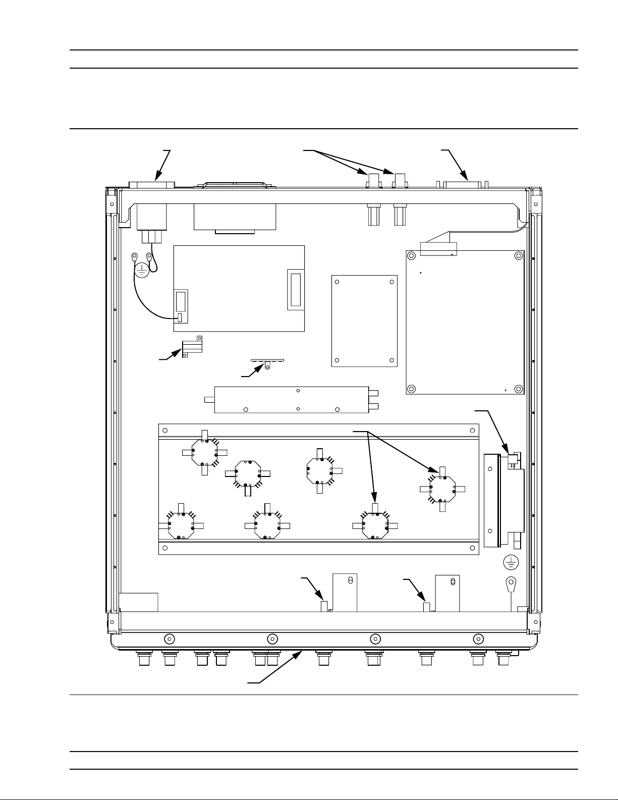
parts are listed in Table 2-1, following page. The locations of these as
semblies/parts are shown in Figure 2-1 on page 2-3.
-
2-2 EXCHANGE ASSEMBLY
PROGRAM
Anritsu maintains a module exchange program for selected
subassemblies. If a malfunction occurs in one of these subassemblies,
the defective item can be exchanged. Upon receiving your request,
Anritsu will ship the exchange subassembly to you,typically within 24
hours. You then have 45 days in which to return the defective item. All
exchange subassemblies or RF assemblies are warranted for 90 days
from the date of shipment,or for the balance of the original equipment
warranty, whichever is longer.
NOTE
Please have the exact model number and serial number of
your unit available when requesting this service,as the
information about your unit is filed according to the
instrument’s model and serial number.For more
information about the program, contact your local sales
representative or call Anritsu Customer Service direct
(refer to Section 2-4).
MN4790A MM 2-1
Page 18

REPLACEABLE SUBASSEMBLIES AND PARTS REPLACEABLE PARTS
2-3 REPLACEABLE
SUBASSEMBLIES AND
PARTS
Table 2-1. Replaceable Subassemblies
Part Number Description Location (Figure 2-1)
1020-46 SP3T Switch S1 and S7
1020-47 SPDT Switch S2 to S6
1091-346 Combiner A2
2000-989 GPIB Interface Assembly A1
40-159 Power Supply A6
SC6737 Bias Tee Assembly A4 and A5
ND60327 Fan Assembly FAN
43045-3 Control PCB Assembly A7
339H40998A Step Attenuator A3
B45259 N Type Test Port Connector N-Connectors
2-4 PARTS ORDERING
INFORMATION
Table 2-1 lists the major replaceable subassemblies and parts for the
MN4790A. These assemblies and parts are presently covered by the
Anritsu exchange assembly program.
All parts listed in Table 2-1 may be ordered from your local Anritsu
service center (Table 1-2,page 1-8).Or, they may be ordered directly
from the factory at the following address:
Anritsu Company
ATTN: Customer Service
490 Jarvis Drive
Morgan Hill,CA 95037-2809
Telephone: (408)-778-2000
FAX: (408)-778-0239
2-2 MN4790A MM
Page 19
REPLACEABLE PARTS PARTS ORDERING INFORMATION
LINE
MODULE
POWER SUPPLY
POWER
SUPPLY
LOAD
SOLDER JUNCTION
J3
J2
S1
J1
COMM
J2
S6
RBS A/B DC BIAS
SOURCE/FUSE
FAN
A6
COMBINER
RF PIN SWITCHES (7)
COMM
COMM
S3
J2
J1
J1
J1
S2
J2
CONTROL
A2
J2
COMM
S4
J1
J2
GPIB
CONNECTOR
PCB
A7
ATTENUATOR
COMM
S5
J1
GPIB
PARALLEL
INTERFACE
PCB
A1
J1
S7
J2
J3
A3
RBS A
BIAS
TEE
A4
Figure 2-1. MN4790A Major Assemblies Location Diagram (Top View)
RBS B
BIAS
TEE
A5
MN4790A MM 2-3
Page 20
PARTS ORDERING INFORMATION REPLACEABLE PARTS
A6
A1
A7
A2
A3
A4
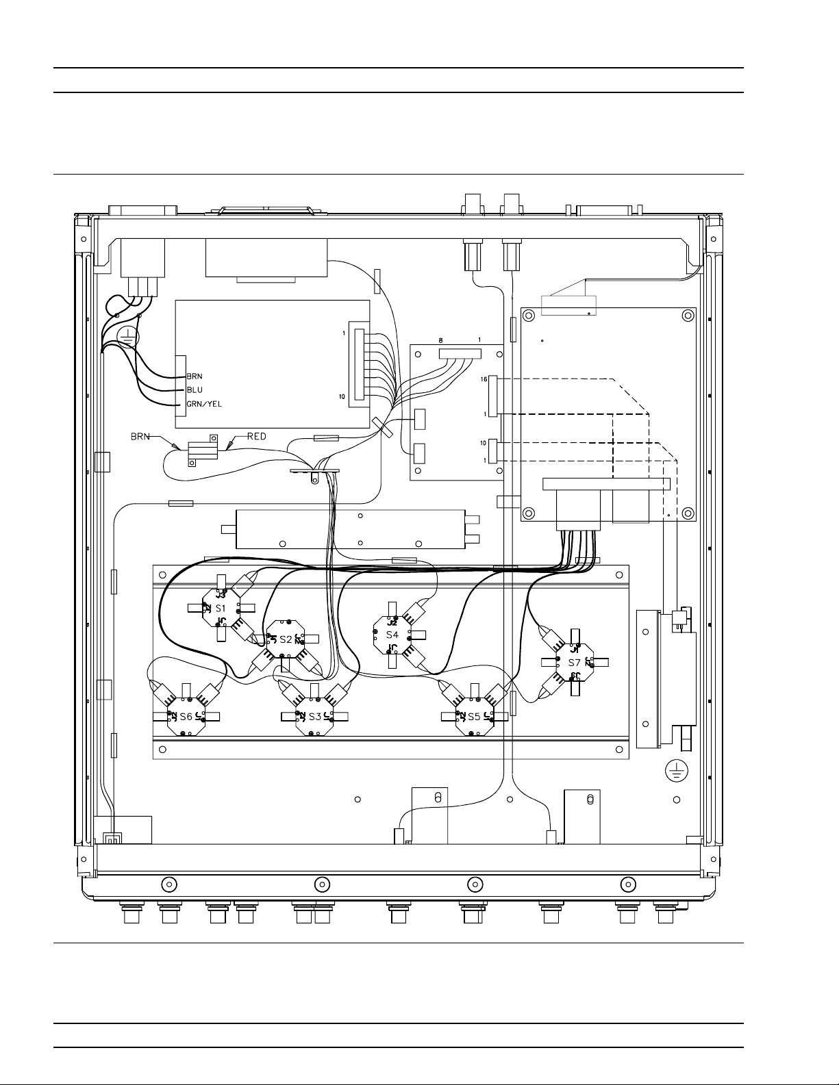
Figure 2-2. MN4790A Wiring Diagram (Top View)
2-4 MN4790A MM
A5
Page 21
REPLACEABLE PARTS PARTS ORDERING INFORMATION
A6
A2
A7
A1
A3
A4
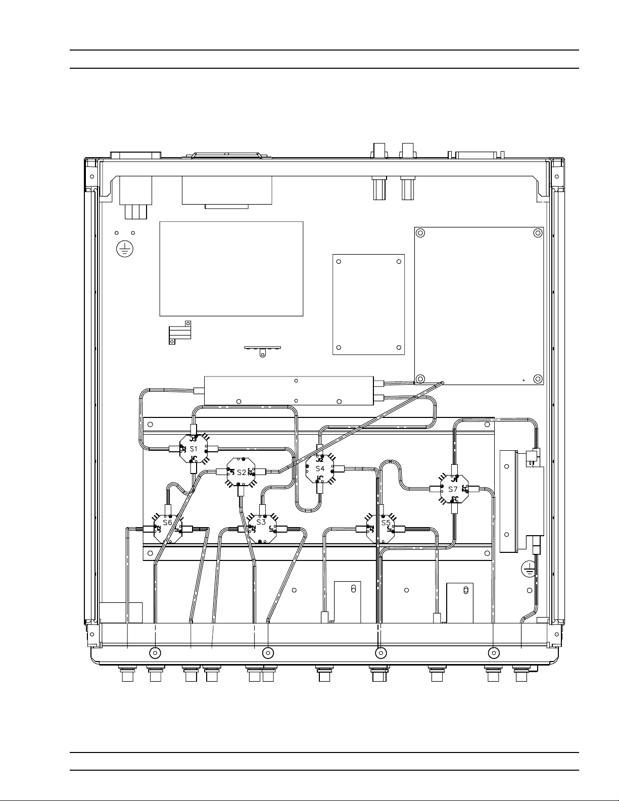
Figure 2-3. MN4790A RF Cabling Diagram (Top View)
MN4790A MM 2-5/2-6
A5
Page 22

Page 23

Chapter 3 Performance Verification Procedure
3-1 INTRODUCTION This chapter provides test procedures to verify the performance of the
Tower Mounted Amplifier Test System. The following tests should be
used to verify the performance of the equipment:
MS4623B VNMS Performance Verification
q
ME7842B (MS4623B and MN4790A) TMATS Performance Verifi
q
cation
3-2 CONVENTIONS The test instructions in this chapter will direct the use of the front
panel hard-keys and soft-keys of the MS4623B.These hard-keys and
soft-keys are distinguished by a different typeface. For example:
Step 1. Press the Utility key and select:
DIAGNOSTICS
TROUBLESHOOTING
MORE
VERIFY ALC CALIBRATION
The Utility key is a front panel hard-key and the DIAGNOSTICS,
TROUBLESHOOTING, MORE, and VERIFY ALC CALIBRATION keys
are all soft-keys.
3-3 PRELIMINARY The following information describes the preliminary setup and
indicates the general tests that verify the performance of your test
system. It is important to first verify the performance of the MS4623B
separate from TMATS.
-
MS4623B VNMS Prior to performing any of the MS4623B performance verification
tests, disconnect the RF cables linked between the front panels of the
MS4623B and the MN4790A test set.
Follow the procedures in Chapter 2 of the MS462XX Vector Network
Measurement Systems Maintenance Manual (part number
10410-00205) to verify that the MS4623B is working properly.
MN4790A MM 3-1
Page 24

PRELIMINARY PERFORMANCE VERIFICATION
ME7842B TMATS Prior to performing any of the ME7842B TMATSperformance
verification tests:
Install the Scorpion Navigator Software on the PC controller
q
Connect the RF cables between the MS4623B and the MN4790A
q
test set.
The ME7842B Performance Verification includes the following tests:
Directivity and Test Port Match Verification
q
Dynamic Range Verification
q
IMD Measurement Operational Checkout
q
Required Equipment The following equipment list is required for all test set verification
tests in this chapter:
Anritsu MS4623B Vector Network Measurement System
q
Anritsu 15NN50-0.6B or 3670NN50-2 Test Port Cable
q
Personal Computer with a Windows Operating System, Scorpion
q
Navigator, and a National Instruments GPIB Interface Installed
The following is an addition requirement for the dynamic range verification:
q
Anritsu 3753LF or 3753R N Connector Calibration Kit
The following are additional requirements for the directivity and test
port match verifications:
q
Anritsu 3753LF or 3753R N Connector Calibration Kit
q
Anritsu 18N50 or SC3833 Air Line
q
Anritsu 29A50-20 Offset Termination (2)
q
Anritsu 22A50 Open/Short
Preliminary Setup Turn on the MS4623B and the MN4790A test set and allow them to
warm up for 30 minutes.
Step 1. Connect a GPIB cable between the IEEE488.2 port of the MS4623B
and the GPIB port of the MN4790A test set.
Step 2. Connect a GPIB cable between the IEEE488.2 port of the MS4623B
and the GPIB interface of the PC controller.
3-2 MN4790A MM
Page 25

PERFORMANCE VERIFICATION PRELIMINARY
Step 3. On the PC, open the Windows Explorer program and locate the execut
able ‘MN4790A.exe’ in the ‘C:\Program Files\Navigator’ folder, as
shown in Figure 3-1.
-
Figure 3-1. Starting the MN4790A
Step 4. Move the mouse pointer to highlight MN4790A.exe and double click to
open the program. A GPIB configuration window, below, will be
displayed.
Step 5. If the GPIB address of the MN4790A test set is four,then click the OK
button. If not, move the slide to select a GPIB address that matches
the GPIB address of the MN4790A test set,then click the OK button.
NOTE
The GPIB address of the MN4790A test set is configured
via the dip switch jumper block located above the GPIB
MN4790A MM 3-3
Page 26

PRELIMINARY PERFORMANCE VERIFICATION
port connector on the rear panel. Figure 3-2 shows the dip
switch setting for a GPIB address of four.
Figure 3-2. GPIB Dip Switch Block for the MN4790A
After selecting the GPIB address, the MN4790A Switch Control win
dow, below,will be displayed.
-
Step 6. This window allows you to select different switched signal paths by
using pre-defined cases. Refer to Table A-1 in the ME7842B operation
manual for definitions of the switched signal path for each case.
NOTE
The scroll bar under the Step Attenuation reference allows
you to change the step attenuator in 10 dB increments.
3-4 MN4790A MM
Page 27

PERFORMANCE VERIFICATION DIRECTIVITY AND TEST PORT MATCH
3-4 DIRECTIVITY AND TEST
PORT MATCH
Test Procedure
Step 1. Follow the preliminary setup procedures on pages 3-2 through 3-4.
Step 2. Click on the Case3 button in MN4790A Switch Control window. This
Step 3. On the MS4623B, press the Default key, then the 0 key to reset the in-
Step 4. Insert the Calibration Component Coefficients diskette into the floppy
This procedure verifies the corrected directivity and test port match of
the:
ANT A Port
q
RBS A Port
q
ANT B Port
q
RBS B Port
q
will configure the switches in the MN4790A test set to allow the sig
-
nals to go through the following paths:
Test Port 1 to the ANT A Port (bypassing the internal combiner)
q
Test Port 2 to the RBS A Port
q
Test Port 3 to the Bypass Port
q
strument.
drive of the MS4623B.
Step 5. Press the Cal key and select:
MORE
COMPONENT UTILITIES
INSTALL KIT INFO FROM FLOPPY DISK
Step 6. Allow the instrument to completely load the data, then select:
RETURN
PERFORM CAL 2 PORT
NEXT CAL STEP
REFLECTION ONLY
BOTH PORTS (S11, S22)
NORMAL (1601 POINTS MAXIMUM)
DATAPOINTS
801 MAX PTS
NEXT CAL STEP
Step 7. Verify that the PORT 1 CONN and PORT2 CONN are TYPE N (F), (If
not, press the PORT 1 CONN or PORT 2 CONN soft-key to change the
connector type.) then select:
START CAL
MN4790A MM 3-5
Page 28

DIRECTIVITY AND TEST PORT MATCH PERFORMANCE VERIFICATION
Step 8. When prompted by the MS4623B, connect the associated calibration
components from the calibration kit to the ANT A port for Test Port 1
and to the RBS A port for Test Port 2. Select MEASURE BOTH PORTS
to continue.
Step 9. After the calibration is complete, press the Enter key to continue.
Step 10. Press the Display key and select:
DISPLAY MODE
SINGLE CHANNEL
RETURN
GRAPH TYPE
LOG MAGNITUDE
Step 11. Connect the N male connector end of the air line to the ANT A port
and terminate the GPC-7 end of the air line with the short.
Step 12. Press the Display key and select AUTO SCALE.
Step 13. Press the Marker key and select READOUT MARKERS.
Step 14. Turn on Marker 1, Marker 2, and Marker 3.
Step 15. Using the rotary knob,position Marker 1 and Marker 2 to adjacent
peaks of the ripple with the greatest negative trough (or to adjacent
troughs if the ripple has the greatest positive peak).
3-6 MN4790A MM
Page 29

PERFORMANCE VERIFICATION DIRECTIVITY AND TEST PORT MATCH
Step 16. Position Marker 3 to the bottom of the trough (or to the top of the peak
if the ripple has the greatest positive peak).Refer to Figure 3-3, below.
Figure 3-3. Log Magnitude Display Plot
Step 17. Sum the values of the two markers (Marker 1 and Marker 2) at the
peaks (or troughs) and divide the result by two. This is the average
value of the two peaks (or troughs). Refer to the example formula be
low:
-+-
23001 22958
MM
+
AverageValue
Record this average value.
Step 18. Record the Marker 3 value.
Step 19. Find the absolute difference of the values recorded in Steps 17 and 18
as follows:
|M3|–|AverageValue |= 23.279 – 22.980 = 0.299
This is the peak-to-peak ripple value. Use an RF measurement chart
(page 3-10) to find the corresponding return loss value. This is the
measured effective test port match.Verify that the test port match is
better than 35 dB.
12
=
2
(. )(. )
=
2
=-
22980
.
-
MN4790A MM 3-7
Page 30

DIRECTIVITY AND TEST PORT MATCH PERFORMANCE VERIFICATION
Step 20. Remove the short and connect the 29A50-20 offset termination to the
GPC-7 end of the air line.
Step 21. Press the Display key and select AUTO SCALE.
Step 22. Find the largest ripple between 10 MHz and 3 GHz.
Step 23. Repeat Steps 15 through 19.
Step 24. Find the corresponding 1+Xor 1–Xvalue from the RF measurement
chart. Use the following formula to calculate the effective directivity
value:
For ripple with a negative trough:
Effective Directivity =
Return Loss value + |(Marker 3 value)| - |(1 - X value)|
For ripple with a positive peak:
Effective Directivity =
Return Loss value + |(Marker 3 value)| + |(1 + X value)|
Step 25. Verify that the directivity is better than 40 dB from 10 MHz to 3 GHz.
Step 26. Find the largest ripple between 3 GHz and 6 GHz.
Step 27. Repeat Steps 23 through 24 and verify that the effective directivity is
better than 35 dB from 3 GHz to 6 GHz.
Step 28. Press the Ch 4 key,then the Display key.
Step 29. Select:
GRAPH TYPE
LOG MAGNITUDE
RETURN
Step 30. Remove the air line from the ANT A port and connect it to the RBS A
port. Terminate the GPC-7 end of the air line with the short.
Step 31. Repeat Steps 14 through 27.
Step 32. On the PC, click the Case4 button on the MN4790A Switch Control
window. This will configure the switches in the MN4790A test set to
allow signals to go through the following paths:
q
Test Port 1 to the ANT B Port (Bypassing the internal combiner)
q
Test Port 2 to the RBS B Port
q
Test Port 3 to the Bypass Port
Step 33. On the MS4623B, press the Cal key and select REPEAT PREVIOUS
CAL.
3-8 MN4790A MM
Page 31

PERFORMANCE VERIFICATION DIRECTIVITY AND TEST PORT MATCH
Step 34. When prompted by the MS4623B, connect the associated calibration
components from the calibration kit to the ANT B port for Test Port 1
and to the RBS B port for Test Port 2. Select MEASURE BOTH PORTS
to continue.
Step 35. After the calibration is complete, press the Enter key to continue.
Step 36. Press the Ch 1 key.
Step 37. Connect the N male connector end of the air line to the ANT B port
and terminate the GPC-7 end of the air line with the short.
Step 38. Repeat Steps 12 through 31.
Step 39. Press the Ch 4 key.
Step 40. Remove the air line from the ANT B port and connect it to the RBS B
port. Terminate the GPC-7 end of the air line with the short.
Step 41. Repeat Steps 12 through 31.
Table 3-1, below, shows the test port match and directivity specifications. Table 3-2, following page, shows the RF measurement chart.
Table 3-1. Test Port Match and Directivity Specifications
Specifications ANT A RBS A ANT B RBS B
Test Port Match
10 MHz to 6 GHz
Directivity
10 MHz to 3 GHz
Directivity
3 GHz to 6 GHz
35 dB
40 dB
35 dB
MN4790A MM 3-9
Page 32

DIRECTIVITY AND TEST PORT MATCH PERFORMANCE VERIFICATION
Table 3-2. RF Measurement Chart
The first three columns are conversion
tables for return loss, reflection coefficient,
and SWR.
The last four columns are values for
interactions of a small phasor X with a
large phasor (unity reference) expressed
in dB related to the reference.
The RF Measurement Chart can be used
to determine the uncertainty due to
bridge/autotester VNA directivity. The
“X dB Below Reference” column
represents the difference between the
directivity and the measured reflection
(return loss). The “Ref + X dB” and
“Ref – X dB” values are 360°. Therefore,
the peak-to-peak ripple (1 ± X) is the total
measurement uncertainty caused by the
error signal.
For example, if a 30 dB return loss is
measured with a 40 dB directivity
autotester, the X dB Below Reference
value is 10 dB. The Ref+XdBvalue is
2.3866 dB and the Ref–XdBvalue is
3.3018 dB.
The actual return loss is between
27.6134 dB (– 30 + 2.3866) and
33.3018 dB (– 30 – 3.3018). The
peak-to-peak ripple on a swept
measurement will be 5.6884 dB. If the
error and directivity signals are equal, the
Ref+XdBvalue equals 6 dB (voltage
doubling causesa6dBchange) and the
Ref–XdBvalue becomes infinite, since
the two signals are equal in amplitude and
180° out of phase (zero voltage).
(Ref + X)
X
(Ref - X)
(Ref)
Phasor Interaction
SWR
17.3910 0.8913 1 1 5.5350 -19.2715 24.8065
8.7242 0.7943 2 2 5.0780 -13.7365 18.8145
5.8480 0.7079 3 3 4.6495 -10.6907 15.3402
4.4194 0.6310 4 4 4.2489 -8.6585 12.9073
3.5698 0.5623 5 5 3.8755 -7.1773 11.0528
3.0095 0.5012 6 6 3.5287 -6.0412 9.5699
2.6146 0.4467 7 7 3.2075 -5.1405 8.3480
2.3229 0.3981 8 8 2.9108 -4.4096 7.3204
2.0999 0.3548 9 9 2.6376 -3.8063 6.4439
1.9250 0.3162 10 10 2.3866 -3.3018 5.6884
1.7849 0.2818 11 11 2.1567 -2.8756 5.0322
1.6709 0.2512 12 12 1.9465 -2.5126 4.4590
1.5769 0.2239 13 13 1.7547 -2.2013 3.9561
1.4985 0.1995 14 14 1.5802 -1.9331 3.5133
1.4326 0.1778 15 15 1.4216 -1.7007 3.1224
1.3767 0.1585 16 16 1.2778 -1.4988 2.7766
1.3290 0.1413 17 17 1.1476 -1.3227 2.4703
1.2880 0.1259 18 18 1.0299 -1.1687 2.1986
1.2528 0.1122 19 19 0.9237 -1.0337 1.9574
1.2222 0.1000 20 20 0.8279 -0.9151 1.7430
1.1957 0.0891 21 21 0.7416 -0.8108 1.5524
1.1726 0.0794 22 22 0.6639 -0.7189 1.3828
1.1524 0.0708 23 23 0.5941 -0.6378 1.2319
1.1347 0.0631 24 24 0.5314 -0.5661 1.0975
1.1192 0.0562 25 25 0.4752 -0.5027 0.9779
1.1055 0.0501 26 26 0.4248 -0.4466 0.8714
1.0935 0.0447 27 27 0.3796 -0.3969 0.7765
1.0829 0.0398 28 28 0.3391 -0.3529 0.6919
1.0736 0.0355 29 29 0.3028 -0.3138 0.6166
1.0653 0.0316 30 30 0.2704 -0.2791 0.5495
1.0580 0.0282 31 31 0.2414 -0.2483 0.4897
1.0515 0.0251 32 32 0.2155 -0.2210 0.4365
1.0458 0.0224 33 33 0.1923 -0.1967 0.3890
1.0407 0.0200 34 34 0.1716 -0.1751 0.3467
1.0362 0.0178 35 35 0.1531 -0.1558 0.3090
1.0322 0.0158 36 36 0.1366 -0.1388 0.2753
1.0287 0.0141 37 37 0.1218 -0.1236 0.2454
1.0255 0.0126 38 38 0.1087 -0.1100 0.2187
1.0227 0.0112 39 39 0.0969 -0.0980 0.1949
1.0202 0.0100 40 40 0.0864 -0.0873 0.1737
1.0180 0.0089 41 41 0.0771 -0.0778 0.1548
1.0160 0.0079 42 42 0.0687 -0.0693 0.1380
1.0143 0.0071 43 43 0.0613 -0.0617 0.1230
1.0127 0.0063 44 44 0.0546 -0.0550 0.1096
1.0113 0.0056 45 45 0.0487 -0.0490 0.0977
1.0101 0.0050 46 46 0.0434 -0.0436 0.0871
1.0090 0.0045 47 47 0.0387 -0.0389 0.0776
1.0080 0.0040 48 48 0.0345 -0.0346 0.0692
1.0071 0.0035 49 49 0.0308 -0.0309 0.0616
1.0063 0.0032 50 50 0.0274 -0.0275 0.0549
1.0057 0.0028 51 51 0.0244 -0.0245 0.0490
1.0050 0.0025 52 52 0.0218 -0.0218 0.0436
1.0045 0.0022 53 53 0.0194 -0.0195 0.0389
1.0040 0.0020 54 54 0.0173 -0.0173 0.0347
1.0036 0.0018 55 55 0.0154 -0.0155 0.0309
1.0032 0.0016 56 56 0.0138 -0.0138 0.0275
1.0028 0.0014 57 57 0.0123 -0.0123 0.0245
1.0025 0.0013 58 58 0.0109 -0.0109 0.0219
1.0022 0.0011 59 59 0.0097 -0.0098 0.0195
1.0020 0.0010 60 60 0.0087 -0.0087 0.0174
Reflection
Coefficient
Return
Loss
(dB)
XdB
Below
Reference
Relative to Unity Reference
Ref+X
(dB)
Ref-X
(dB)
Ref ± X
Pk to Pk Ripple
(dB)
3-10 MN4790A MM
Page 33

PERFORMANCE VERIFICATION DYNAMIC RANGE
3-5 DYNAMIC RANGE This procedure verifies the dynamic range of the:
ANT A Port to the RBS A Port
q
ANT B Port to the RBS B Port
q
Bypass Port to the RBS B Port
q
Test Procedure
Step 1. Follow the preliminary setup procedures on pages 3-2 through 3-4.
Step 2. Click on the Case3 button in MN4790A Switch Control window. This
will configure the switches in the MN4790A test set to allow the
signals to go through the following paths:
Test Port 1 to the ANT A Port (bypassing the internal combiner)
q
Test Port 2 to the RBS A Port
q
Test Port 3 to the Bypass Port
q
Step 3. On the MS4623B, press the Default key, then the 0 key to reset the in-
strument.
Step 4. Press the Ch 3 key,then the Display key.
Step 5. Select:
DISPLAY MODE
SINGLE CHANNEL
RETURN
GRAPH TYPE
LOG MAGNITUDE
Step 6. Press the Avg key and select:
SELECT I.F. BANDWIDTH
I.F.BW 10Hz
Step 7. Connect a test port cable between the ANT A port and the RBS A port.
Wait until one sweep has completed.
Step 8. Press the Display key and select:
TRACE MEMORY
STORE DATA TO MEMORY
VIEW DATA(/) MEMORY
RETURN
SCALE
Step 9. Change the REFERENCE VALUE to -80 dB.
Step 10. Disconnect the cable from the ANT A port.
MN4790A MM 3-11
Page 34

DYNAMIC RANGE PERFORMANCE VERIFICATION
Step 11. Connect the offset terminations to the ANT A port and to the open end
of the cable.
Step 12. Verify that the displayed trace is below -75 dB from 10 MHz to
50 MHz and below -80 dB from 50 MHz to 6 GHz.
Step 13. On the PC, click the Case4 button in the MN4790A Switch Control
window. This will configure the switches in the MN4790A test set to
allow the signals to go through the following paths:
Test Port 1 to the ANT B Port (bypassing the internal combiner)
q
Test Port 2 to the RBS B Port
q
Test Port 3 to the Bypass Port
q
Step 14. Connect the test port cable between the ANT B port and the RBS B
port. Wait until one sweep has completed.
Step 15. On the MS4623B, press the Display key and select:
TRACE MEMORY
STORE DATA TO MEMORY
VIEW DATA(/) MEMORY
Step 16. Disconnect the cable from the ANT B port.
Step 17. Connect the offset terminations to the ANT B port and to the open end
of the cable.
Step 18. Verify that the displayed trace is below -75 dB from 10 MHz to
50 MHz and below -80 dB from 50 MHz to 6 GHz.
Step 19. Press the Meas key and select:
MORE
S23, TRANS b1/a3
Step 20. Disconnect the terminations from the ANT B port and from the open
end of the cable. Connect the open end of the cable to the Bypass port.
Wait until one sweep has completed.
Step 21. Press the Display key and select:
TRACE MEMORY
STORE DATA TO MEMORY
VIEW DATA(/) MEMORY
Step 22. Disconnect the cable from the Bypass port.
Step 23. Connect the offset termination to the Bypass port and to the open end
of the cable.
3-12 MN4790A MM
Page 35

PERFORMANCE VERIFICATION DYNAMIC RANGE
Step 24. Verify that the displayed trace is below -80 dB.
Table 3-3. Dynamic Range Test Specifications
Dynamic Range Between Ports Specification Measured
ANT A and RBS A
10 MHz to 50 MHz
50 MHz to 6 GHz
ANT B and RBS B
10 MHz to 50 MHz
50 MHz to 6 GHz
Bypass and RBS B
10 MHz to 6 GHz 80 dB
75 dB
80 dB
75 dB
80 dB
MN4790A MM 3-13
Page 36

IMD MEASUREMENT PERFORMANCE VERIFICATION
3-6 IMD MEASUREMENT This procedure verifies that the IMD measurement signal path is op
erational.
Test procedure
Step 1. Follow the preliminary setup procedures on pages 3-2 through 3-4.
Step 2. Click on the Case1 button in the MN4790A Switch Control window.
This will configure the switches in the MN4790A test set to allow the
signals to go through the following paths:
Test Port 1 to the ANT A Port (through the combiner)
q
Test Port 3 to the ANT A Port (through the combiner)
q
Test Port 2 to the RBS A Port
q
Step 3. On the MS4623B, press the Default key, then the 0 key to reset the in
strument.
Step 4. Press the Appl key and select:
CHANGE APPLICATION SETUP
MEASUREMENT TYPE
IMD
Step 5. Press the Display key and select:
-
-
DISPLAY MODE
SINGLE CHANNEL
RETURN
GRAPH TYPE
LOG MAGNITUDE
Step 6. Connect a test port cable between the ANT A port and the RBS A port.
Step 7. Press the Appl key and select:
SWEEP MODE: CW RCVR
DISPLAY SELECTION: PRODUCT
RETURN
TONE 2 OFFSET: 301 kHz
Step 8. Press the Freq key and select:
CW MODE ON
Step 9. Change the CW frequency to 869 MHz.
Step 10. Press the Display key and select:
AUTO SCALE
3-14 MN4790A MM
Page 37

PERFORMANCE VERIFICATION IMD MEASUREMENT
Step 11. Press the Avg key and select:
SELECT I.F. BANDWIDTH
I.F.BW 10Hz
Step 12. Press the Marker key and select:
READOUT MARKERS
Step 13. Select the soft-key next to the 1:, 2:, 3:,and 4: markings to turn on
these markers. Use the rotary knob to move:
Marker 1 to the peak of Tone 1
q
Marker 2 to the peak of Tone 2
q
Marker 3 to the peak left of Tone 1
q
Marker 4 to the peak right of Tone 2
q
Step 14. Select the soft-key next to the 1: marking so that Marker 1 is now the
active marker (distinguished by a square surrounding the marker
number). See Figure 3-4.
Figure 3-4. Log Magnitude Display Plot
Step 15. Press the Marker key and select:
DREF MODE: ON
READOUT MARKERS
MN4790A MM 3-15
Page 38

IMD MEASUREMENT PERFORMANCE VERIFICATION
Step 16. Verify that the (1-2) reading is less than 2 dB and that the (1-3) and
(1-4) readings are less than 60 dB (see Figure 3-5).
Figure 3-5. Log Magnitude Display Plot
3-16 MN4790A MM
Page 39

Chapter 4 Troubleshooting
4-1 INTRODUCTION The tests in this section provide a method of testing the MN4790A test
set for proper operation. These tests are intended to be used as
troubleshooting tools for checking the operational functionality of the
components in the MN4790A.
4-2 OPERATIONAL CHECK Operational tests for the MN4790A consists of the following:
Internal Signal Path Insertion Loss Check
q
Test Channel Step Attenuator Check
q
NOTE
Prior to performing these tests, the MS4623B must be verified to be in good condition. Follow the procedures in
Chapter 2 of the MS462XX Vector Network Measurement
Systems Maintenance Manual (part number 10410-00205)
to verify that the MS4623B is working properly.
Required Equipment
q
Anritsu MS4623B Vector Network Measurement System
4-3 INTERNAL SIGNAL PATH
INSERTION LOSS CHECK
Test Setup
Step 1. Follow the preliminary setup procedures on pages 3-2 through 3-4.
Step 2. On the MS4623B, connect a through cable to Port 1 and a second
q
Anritsu 3753R or 3753LF N Connector Type Calibration Kit
q
Anritsu 33NN50B (from 3753R/1) or 34NN50A Adapter
q
Anritsu 3670NN50-2 Through Cable or Equivalent
q
Anritsu 3670N50-2 Through Cable or Equivalent
q
Anritsu 2100-2 GPIB Interface Cable
q
Personal Computer with a Windows Operating System, Scorpion
Navigator, and a National Instruments GPIB Interface Installed
This test checks the insertion loss of various switched signal paths. If
the measured insertion loss is improperly high, then a RF component
in that signal path may be defective.
through cable to Port 2.
MN4790A MM 4-1
Page 40

INTERNAL SIGNAL PATH INSERTION LOSS CHECK TROUBLESHOOTING
Step 3. Perform a Forward Path Transmission Frequency Response calibra
tion from 10 MHz to 6 GHz with 401 data points.
Step 4. Set up the MS4623B display to:
SINGLE CHANNEL
S21
LOG MAGNITUDE
Test Procedure This test procedure is illustrated in Table 4-1.
Step 1. For each test sequence, click on the appropriate “Case” button in the
Switch Control window
Step 2. Connect the through cables to the appropriate ports of the test system
and measure the insertion loss of the pre-set signal path per Table 4-1.
Table 4-1. Internal Signal Path Insertion Loss Test Sequences
Test
Sequence
A Case3 Test Port 1 of the
B Case3 Test Port 3 of the
C Case3 RBS A Port of the
D Case4 Test Port 1 of the
E Case4 RBS B Port of the
F* Case1 Test Port 1 of the
G* Case1 Test Port 3 of the
H Case20 Aux In 1 Port of the
I Case19 Aux In 2 Port of the
J Case21 RBS A Port of the
K Case8 RBS B Port of the
* Measure Insertion Loss from 500 MHz to 6 GHz only.
Case Button
Connect Port 1 of
the MS4623B to
MN4790A
MN4790A
MN4790A
MN4790A
MN4790A
MN4790A
MN4790A
MN4790A
MN4790A
MN4790A
MN4790A
Connect Port 2 of
the MS4623B to
ANT A Port of the
Bypass Port of the
Test Port 2 of the
ANT B Port of the
Test Port 2 of the
ANT A Port of the
ANT A Port of the
ANT B Port of the
ANT A Port of the
Aux Out 1 Port of the
Aux Out 2 Port of the
MN4790A
MN4790A
MN4790A
MN4790A
MN4790A
MN4790A
MN4790A
MN4790A
MN4790A
MN4790A
MN4790A
Measured
Insertion Loss
-
Maximum Allowable
Insertion Loss
15 dB
15 dB
15 dB
15 dB
15 dB
15 dB
15 dB
15 dB
15 dB
15 dB
15 dB
Step 3. Refer to Table 4-2,following page, for solutions to any of the insertion
loss tests failures
4-2 MN4790A MM
Page 41

TROUBLESHOOTING INTERNAL SIGNAL PATH INSERTION LOSS CHECK
Table 4-2. Internal Signal Path Insertion Loss Test Sequence Failure Solutions
Test Sequence Failure Solutions
A Replace Switches S3, S1 or S4
B Replace Switch S2
C Replace Switches S5, S7 or Step Attenuator
D Replace Switch S3
E Replace Switches S5, S7 or Step Attenuator
F Replace Switch S4 or Combiner
G Replace Switch S2 or Combiner
H Replace Switch S6
I Replace Switch S6
J Replace Switches S5 or S7
K Replace Switches S5 or S7
MN4790A MM 4-3
Page 42

TEST CHANNEL STEP ATTENUATOR CHECK TROUBLESHOOTING
4-4 TEST CHANNEL STEP
ATTENUATOR CHECK
Test Setup
Step 1. Follow the preliminary setup procedures on pages 3-2 through 3-4.
Step 2. On the MS4623B, press the Default key, then the 0 key to reset the
Step 3. Press the Display key.
Step 4. Select:
Step 5. Press the Ch 3 key, then the Display key.
Step 6. Select:
Step 7. Press the Avg key.
This test checks that the Test Channel Step Attenuator functions
properly.
instrument.
DISPLAY MODE
SINGLE CHANNEL
RETURN
GRAPH TYPE
LOG MAGNITUDE
RETURN
Step 8. Select:
Step 9. Connect a through cable between Port 1of the MS4623B and the
Test Procedure
Step 1. On the PC controller, select the Case3 button in the MN4790A Switch
Step 2. On the MS4623B, select:
Step 3. Allow the trace to sweep twice, then select:
SELECT I.F. BANDWIDTH
I. F. BW 10 Hz
RBS A port of the MN4790A. Connect a second through cable between
Port 2 of the MS4623B and Test Port 2 of the MN4790A.
Control window.
TRACE MEMORY
STORE DATA TO MEMORY
VIEW DATA(/) MEMORY
RETURN
4-4 MN4790A MM
Page 43

TROUBLESHOOTING TEST CHANNEL STEP ATTENUATOR CHECK
Step 4. Select:
SCALE
10 dB/DIV
Step 5. On the PC, position the mouse pointer to the scroll bar on the right
hand side of the MN4790A Switch Control window.Right-click to move
the pointer downward and change the attenuation setting to 10 dB.
Step 6. Verify that the displayed S21 trace is within the range specified in Ta
ble 4-3.
Step 7. Repeat Steps 5 and 6 for the other specified attenuation levels in Ta
ble 4-3.
Table 4-3. Step Attenuator Specifications
Step Attenuator Setting Attenuation Specification (dB)
10 10 ± 1
20 20 ± 1
30 30 ± 2
40 40 ± 2
50 50 ± 2
60 60 ± 3
70 70 ± 3
Step 8. If the test result is out of the expected range,replace the step attenu
ator.
-
-
-
MN4790A MM 4-5
Page 44

TROUBLESHOOTING TROUBLESHOOTING
4-5 TROUBLESHOOTING The following paragraphs provide suggestions for troubleshooting cer
tain test-set components.
Test Set Fails to
Power Up
WARNING
Line Source and
Interface Checks
Step 1. Verify that the ac power source is providing stable power at the correct
If the MN4790A test set fails to power up when connected to an ac
power source and the Power key is pressed,perform the power supply
checks described below.
WARNING
Hazardous voltages are present inside the instrument
when ac line power is connected. Turn off the instrument
and remove the line cord before removing any covers or
panels. Troubleshooting or repair procedures should only
be performed by qualified service personnel who are fully
aware of the potential hazards.
line voltage.
NOTE
The MN4790A is designed to automatically sense and operate with ac line voltages in the range of 85 to 264 VAC,
with a frequency of 47 to 63 Hz.
-
Step 2. Verify that the power input cord is in good condition.
Step 3. Verify that the power line fuse is installed,that it is not blown (open),
Power Supply Voltage
Check
Step 1. Turn off the test set and disconnect the power cord from the instru
Step 2. Remove the top cover.
Step 3. Reconnect the power cord to the test set and turn it on.
and that it is the correct value (1.6A,Slow Blow, part number 631-81).
ment. Ensure that all external cable connections to the test set’s front
and rear panel are also disconnected.
4-6 MN4790A MM
Page 45

TROUBLESHOOTING TROUBLESHOOTING
Step 4. Using a digital multi-meter or oscilloscope, measure the dc power sup
Table 4-1. Power Supply Voltages
Measured Pin Common Pin DC Supply Voltage (V)
TP2 TP1 +5 ± 0.25
TP4 TP1 +15 ± 0.9
ply voltages on the Controller PCB at the test points listed in Ta
ble 4-1 (see to Figure 4-2, below).
-
-
Figure 4-2. A6 Power Supply Test Point Location Diagram
Step 5. If any of the dc voltage tests fail,replace the A6 dc power supply. Refer
to the A6 power supply remove and replace procedures in Chapter 5.
MN4790A MM 4-7/4-8
Page 46

Page 47

Chapter 5 Removal and Replacement Procedures
5-1 INTRODUCTION This chapter provides procedures for removing and reinstalling the
replaceable subassemblies listed in Chapter 2, Table 2-1.
5-2 EQUIPMENT REQUIRED All procedures in this chapter require the use of either a #1 or #2 size
Phillips type screw driver. Most procedures require the use of a
5/16 inch wrench and the Anritsu 01-201 (8 inch-pounds) torque
wrench. Some procedures require the use of a small jewelers Phillips
screwdriver.
CAUTION
Always use a torque wrench calibrated to 8 inch-pounds
when tightening SMA connectors. Over-torquing will cause
damage to the RF connectors.
5-3 REMOVING THE COVERS Troubleshooting operations require removal of the top cover.
Replacement of some test set assemblies and parts require removal of
all covers. The following procedure describes this process.
Preliminary
Step 1. Switch the test set power off and remove the power cord.
Step 2. Remove the test set from the ME7842B test system by disconnecting
all cable connections and separating the test set from the MS4623B.
Procedure Refer to Figure 5-1, page 5-3, during this procedure.
NOTE
It is only necessary to loosen the test set’s front handle
assemblies to remove the top, bottom, or side covers.
However, if the front panel is to be removed, the handle
assemblies should also be removed.
MN4790A MM 5-1
Page 48

REMOVING THE COVERS REMOVE AND REPLACE
Step 3. Loosen (or remove) the right and left handle assemblies, as follows:
a. Place the test set on its top (bottom-side up).
b. Loosen (or remove) the screws at the sides of the handle
assemblies.
c. If removing the handles, pull them away from the unit and set
aside.
CAUTION
The green headed screws have metric
threads. Be sure to retain all of the screws
and replace them in their original location.
Step 4. To remove the top cover:
a. Place the test set in normal (top-side up) position.
b. Remove the feet from the two top corners at the rear of the test
set.
c. Remove the center screw from the rear of the top cover.
d. Lift and slide the top cover away from the test set.
Step 5. To remove the bottom cover:
a. Place the test set on its top (bottom-side up).
b. Remove the feet from the two bottom corners at the rear of the
test set.
c. Remove the center screw from rear of the bottom cover.
d. Lift and slide the bottom cover away from the test set.
Step 6. To remove the right cover:
a. Place the test set on its left side.
b. Remove the feet from the two right-side corners at the rear of
the test set.
c. Remove the center screw from the right cover.
d. Lift and slide the side cover away from the test set.
Step 7. To remove the left cover:
a. Place the test set its right side.
b. Remove the feet from the two left-side corners at the rear of the
test set.
c. Remove the center screw from rear of the left side cover.
d. Lift and slide the side cover away from the test set.
5-2 MN4790A MM
Page 49

Figure 5-1. MN4790A Test Set Cover Removal
To replace the instrument covers, perform the previous steps in the
reverse order.
MN4790A MM 5-3
Page 50

A1 GPIB PARALLEL INTERFACE PCB REMOVE AND REPLACE
5-4 A1 GPIB PARALLEL
INTERFACE PCB
This Section provides a procedure for removing and replacing the A1
GPIB Parallel Interface PCB in the test set.
Step 1. Remove the top cover from the test set (Section 5-3).
Step 2. Disconnect the two cables from connectors J2 and J3. (Figure 5-2).
Step 3. Remove the four mounting screws.
Step 4. Lift the A1 PCB assembly out from the test set chassis.
Remove
Mounting
Screws (4)
Remove
Cables
A6
J3
A1
A7
J2
A2
A3
Figure 5-2. A1 GPIB Parallel Interface PCB Removal
To replace A1 GPIB Parallel Interface PCB, reverse the order of the
removal procedure.
5-4 MN4790A MM
Page 51

REMOVE AND REPLACE A2 COMBINER
5-5 A2 COMBINER This Section provides a procedure for removing and replacing the A2
Combiner in the test set.
Step 1. Remove the top cover from the test set (Section 5-3).
Step 2. Disconnect the three RF cables from the Combiner using a 5/16-inch
wrench (Figure 5-3).
Step 3. Remove the two Combiner mounting screws with a Phillips
screwdriver.
Step 4. Lift the Combiner out from the test set chassis.
Remove RF
Cables (3)
Remove
Mounting
Screws (2)
Figure 5-3. A4 Combiner Removal
A6
A2
A7
A1
A3
To replace combiner, reverse the order in the removal procedure.
MN4790A MM 5-5
Page 52

A3 STEP ATTENUATOR REMOVE AND REPLACE
5-6 A3 STEPATTENUATOR This Section provides a procedure for removing and replacing the A3
Step Attenuator in the test set.
Step 1. Remove the right side cover from the test set (Section 5-3).
Step 2. Disconnect the Step Attenuator ribbon-cable from the Step Attenuator
(Figure 5-4).
Step 3. Disconnect the RF cables from the Step Attenuator using a 5/16-inch
wrench.
Step 4. Remove the two large Step Attenuator mounting screws with a Phil
Step 5. Slide the Step Attenuator out from the test set chassis.
Figure 5-4. A3 Step Attenuator Removal
-
lips screwdriver.
Remove RF Cables
Remove Ribbon Cable
A3
Remove Larger Mounting Screws
To replace the step attenuator, reverse the order of the removal
procedure.
5-6 MN4790A MM
Page 53

REMOVE AND REPLACE A4 AND A5 BIAS TEES
5-7 A4 AND A5 BIAS TEES This Section provides a procedure for removing and replacing the A4
and A5 Bias Tees in the test set.
Step 1. Remove the top cover from the test set (Section 5-3).
Step 2. Unscrew the RBS Bias connectors from the top of the Bias Tee using a
3/16-inch wrench (Figure 5-5).
Step 3. Remove the RF cables from the Bias Tee and the SP3T switch with a
5/16-inch wrench.
Step 4. Remove the Bias Tee mounting screws with a #1 Phillips screwdriver.
Step 5. Unscrew the Bias Tee from the front panel RF connector with a
5/16-inch wrench and remove the Bias Tee.
A6
A2
Remove the
RF Cable
Remove the Mounting Screws,
A7
A1
A3
Unscrew the
RBS Bias Cable
Unscrew the Bias Tee From
the Front Panel RF Connector
Figure 5-5. A4, A5 Bias Tee Removal
To replace the Bias Tee,reverse the order of the removal procedure.
MN4790A MM 5-7
Page 54

A6 POWER SUPPLY REMOVE AND REPLACE
5-8 A6 POWER SUPPLY This Section provides a procedure for removing and replacing the A6
Power Supply in the test set.
Step 1. Remove the top and bottom covers from the test set (Section 5-3).
Step 2. Disconnect all the cable connections from the Power Supply (Fig
ure 5-6).
Step 3. Turn the test set on its side.
Disconnect Power Supply
Input and Ground Connection
Disconnect Power Supply
Output Connection
A6
A7
A2
A1
-
A3
Figure 5-6. A6 Power Supply Removal (Bottom View)
5-8 MN4790A MM
Page 55

REMOVE AND REPLACE A6 POWER SUPPLY
Step 4. Hold the Power Supply and remove the four mounting screws with a
Phillips screwdriver (Figure 5-7).
Step 5. Lift the Power supply out from the test set chassis.
Remove the Power Supply
Mounting Screws
Figure 5-7. A6 Power Supply Removal (Bottom View)
To replace the Power Supply, reverse the order of the removal proce
dure.
-
MN4790A MM 5-9
Page 56

A7 CONTROL PCB REMOVE AND REPLACE
5-9 A7 CONTROL PCB This Section provides a procedure for removing and replacing the A7
Control PCB in test set.
Step 1. Remove the top cover from the test set (Section 5-3).
Step 2. Disconnect the cables on the Control PCB at P1, J1, J2, J3, J4,and J5
(Figure 5-8).
Step 3. Remove the four mounting screws.
Step 4. Lift the Control PCB out from the test set chassis.
Remove Calble
Connections
A6
A2
Remove Mounting
Screws (4)
P1
J4
J1
J5
A7
J3
J2
A1
A3
Figure 5-8. A7 Control PCB Removal
To replace the Control PCB, reverse the order of the removal proce
-
dure.
5-10 MN4790A MM
Page 57

REMOVE AND REPLACE FAN ASSEMBLY
5-10 FAN ASSEMBLY This Section provides a procedure for removing and replacing the rear
panel fan assembly.
Step 1. Remove the top cover from the test set (Section 5-3).
Step 2. Remove the four screws holding the fan guard in place (Figure 5-9).
Step 3. Remove the fan guard and lift out the fan.
Figure 5-9. Fan Removal
To replace the fan,reverse the order of the removal procedure.
MN4790A MM 5-11
Page 58

SP3T AND SPDT SWITCHES REMOVE AND REPLACE
5-11 SP3T AND SPDT
SWITCHES
A6
This Section provides a procedure for removing and replacing the
SP3T and SPDT RF switches.
Step 1. Remove the top cover from the test set (Section 5-3).
Step 2. Disconnect the RF cables from the SP3T or SPDT switch (Figure 5-10).
Step 3. Disconnect the wire connectors from the SP3T or SPDT switch.
Step 4. Remove the four Phillips screws from the SP3T or SPDT switch.
Step 5. Lift the SP3T or SPDT switch out from the test set chassis.
Disconnect
RF Cables
J1 J2
COMM
-5
+5
G
-5
+5
G
A7
A1
L1
L2
G
(Not Used)
Disconnect
Wire Connectors
SPDT
A2
S1
S4
S5
S6
S2
S3
Figure 5-10. SP3T and SPDT RF Switch Removal
To replace the SP3T or SPDT switch, reverse the order of the removal
procedure.
S7
A3
J3
COMM
J2
J1
L3
L2
SP3T
L1
Remove Phillips
Screws Only (4)
S4, S7 S1,S3, S5, S6 S2
5-12 MN4790A MM
Page 59

REMOVE AND REPLACE SP3T AND SPDT SWITCHES
Table 5-1 . SP3T and SPDT RF Switch Wiring Legend
SP3T or SPDT
Switch Number
S1
S2 Orange Red Brown Green Blue Not Used
S3 Orange Red Brown Purple Gray Not Used
S4 Orange Red Brown Black White Not Used
S5 Orange Red Brown Red Brown Not Used
S6 Orange Red Brown Orange Yellow Not Used
S7 Orange Red Brown Green Yellow Blue
Pin –5
Wire Color
Orange Red Brown
Pin +5
Wire Color
Wire Color
Pin G
Pin L1
Wire Color
Brown Red Orange
Pin L2
Wire Color
Pin L3
Wire Color
MN4790A MM 5-13/5-14
Page 60

Page 61

Appendix A
0
1
2
3
4
5
1
2
3
4
2
11
2
Connector Maintenance
Check Procedures
A-1 INTRODUCTION This appendix provides general, precautionary information and in
-
structions pertaining to precision connectors.
A-2 PRECAUTIONS The following paragraphs are precautionary notes relating to mainte
nance considerations for precision connectors
Pin Depth Problems Based on Anritsu precision components returned for repair,
destructive pin depth of mating connectors is the major cause of
REFERENCE
PLANE
PIN
DEPTH
(INCHES)
FEMALE
Figure A-1. N Connector Pin Depth
Definition
REFERENCE
PLANE
(INCHES)
PIN
DEPTH
MALE
failure in the field. When a precision component is mated with a
connector having a destructive pin depth, damage will likely occur to
the precision component’s connector. A connector is considered to have
destructive pin depth when the center pin is too long with respect to
the connector’s reference plane (Figure A-1).
Before mating an unknown or new device with your test set port
connectors or calibration devices, always measure the pin depth of the
device’s connectors. Use an Anritsu Pin Depth Gauge,or equivalent,for
these measurements (Figure A-2). Also, measure the connector pin
depth of a device when intermittent or degraded performance is
suspected.
Gauging sets for measuring the pin depth of precision connectors are
available from your nearest Anritsu service center, or from the factory.
Instructions for measuring connector pin depth are included with the
gauging set.
-
Figure A-2. Pin Depth Gauge
MN4790A MM A-1
Page 62

PRECAUTIONS APPENDIX A
Pin Depth Tolerance The center pin of a precision connector has a tolerances measured in
mils (one mil = 1/1000 inch). The connectors of test devices may not be
precision types and they may not have the proper pin depth. These
connectors should be measured before mating to ensure suitability.
When gauging pin depth, if the connector being measured indicates
out of tolerance in the “+” region of the gauge (Table A-1), the center
pin is too long. Mating under this condition will likely damage the mat
ing connector. On the other hand,if the test device connector indicates
out of tolerance in the “–” region,the center pin is too short. While this
will not cause any damage, it will result in a poor connection and a
consequent degradation in performance.
Table A-1. Connector Pin Depth Tolerance
-
Avoid Over Torquing
Connectors
Teflon Tuning
Washers
Port Connector Type Pin Depth (Mils)
GPC-7
N Male
N Female
3.5 mm Male, Female
K Male, Female
V Male
V Female
207
207
+0.000
–0.003
–0.000
+0.004
–0.004
+0.000
–0.000
+0.002
+0.0000
–0.0035
+0.000
to –0.001
+0.000
to –0.001
Gauge
Reading
Same As
Pin Depth
207
Same As
Pin Depth
+0.000
–0.004
Over torquing connectors is destructive;it may damage the connector
center pin.Finger tight is usually sufficient,especially on Type N con
nectors. Should it be necessary to use a wrench to tighten SMA or
WSMA connectors, use a torque wrench that breaks at 8 inch-pounds.
As a general rule, never use pliers to tighten connectors.
The center conductor on many precision connectors contains a small
Teflon tuning washer located near the point of mating (interface). This
washer compensates for minor impedance discontinuities at the inter
face. The washer’s location is critical to the connector’s performance.
Do not disturb the Teflon Tuning Washer.
-
-
Avoid Mechanical
Shock
Precision connectors are designed to withstand years of normal bench
handling. Do not drop or otherwise treat them roughly. They are labo
ratory-quality devices, and like other such devices, they require careful
handling.
A-2 MN4790A MM
Page 63

APPENDIX A REPAIR AND MAINTENANCE
Keep Connectors
Visual Inspection Precision connectors should be inspected periodically. Check for the
A-3 REPAIR AND
MAINTENANCE
Clean
The precise geometry that makes a precision connector’s high perfor
mance possible can be disturbed by dirt and other contamination ad
hering to connector interfaces. When not in use, keep the connectors
covered.
following:
Bent or broken center pin
q
Damaged threads
q
Other bent or damaged connector parts
q
Dirt or foreign material in connector cavity
q
Anritsu recommends that no maintenance other than cleaning be
attempted by the customer. Any device with a suspected defective
connector should be returned to Anritsu for repair and/or service when
needed.
-
-
MN4790A MM A-3/A-4
Page 64

INDEX A TO D
Index
A
A1 GPIB Parallel Interface PCB
Location····················2-2
Part Number ·················2-2
Replacement ·················5-4
A2 Combiner
Description ··················1-3
Part Number ·················2-2
Replacement ·················5-5
A3 Step Attenuator
Location····················2-2
Part Number ·················2-2
Replacement ·················5-6
A4 Bias Tee
Location····················2-2
Part Number ·················2-2
Replacement ·················5-7
A5 Bias Tee
Location····················2-2
Part Number ·················2-2
Replacement ·················5-7
A6 Power Supply
Location····················2-2
Part Number ·················2-2
Replacement··············5-8to5-9
A7 Control PCB
Location····················2-2
Part Number ·················2-2
Replacement·················5-10
Acrobat Reader ·················1-1
Adobe Acrobat··················1-1
Anritsu Service Centers·············1-8
B
Bias Tee
Location····················2-2
Part Number ·················2-2
Replacement ·················5-7
Block Diagram,TMATS·············1-5
C
CDROM·····················1-1
Cleaning Connectors ··············A-3
Combiner
Description ··················1-3
Location····················2-2
Replacement ·················5-5
Connector Maintenance
Cleaning ···················A-3
Introduction ·················A-1
Mechanical Shock ··············A-2
Pin Depth Problems ·············A-1
Pin Depth Tolerances ············A-2
Precautions··················A-1
Repair/Maintenance ·············A-3
Teflon Tuning Washer ············A-2
Torquing Connectors·············A-2
Visual Inspection···············A-3
Control PCB
Location····················2-2
Part Number ·················2-2
Replacement·················5-10
Conventions for
Front Panel Keys···············3-1
Instrument References············1-1
Menu Keys ··················3-1
Covers, Removing ············5-1to5-2
D
Description
Combiner ···················1-3
Hardware ···················1-2
ME7842B ···················1-2
MN4790A···················1-3
MS4623B ···················1-2
Scorpion····················1-2
System ·················1-2to1-5
Diagram of
Assembly Location ··············2-3
RF Cabling ··················2-5
Wiring·····················2-4
Directivity and Test Port Match Test · 3-5 to 3-10
Dynamic Range Test··········3-11 to 3-13
372XXB MM Index-1
Page 65

E TO P INDEX
E
Electro-Static Discharge Procedures ······1-7
Equipment, Required for
Removing and Replacing Subassemblies · · 5-1
Troubleshooting Tests ············4-1
Verification Tests ···············3-2
Exchange Assembly Program··········2-1
F
Fan Assembly
Location····················2-2
Part Number ·················2-2
Replacement·················5-11
Front Panel View ················1-4
G
GPIB Parallel Interface PCB
Location····················2-2
Part Number ·················2-2
Replacement ·················5-4
H
ME7842B
Preliminary Setup ··············3-2
System Overview···············1-2
Mechanical Shock················A-2
MN4790A
Assembly Location Diagram ·········2-3
Description ··················1-3
Front and Rear Panel View ·········1-4
RF Cabling Diagram ·············2-5
Wiring Diagram ···············2-4
MS4623B
Description ··················1-2
Preliminary Setup ··············3-1
N
Number, Identification ·············1-1
O
Online Manual ·················1-1
Operational Check ···············4-1
Overview
MN4790A···················1-3
TMATS····················1-2
Hardware Description··············1-2
I
Identification Number ·············1-1
IMD Measurement Test········3-14 to 3-16
Insertion Loss Check···········4-1to4-3
Introduction ···················1-1
L
List of
Recommended Test Equipment ·······1-6
Replaceable Subassemblies ·········2-2
Required Equipment for Troubleshooting· · 4-1
Required Equipment for Verification Tests · 3-2
Service Centers················1-8
M
Manual
Online·····················1-1
Scope of ····················1-1
P
Parallel Interface PCB
Location····················2-2
Part Number ·················2-2
Replacement ·················5-4
Parts
Ordering Information ·········2-2to2-5
Pin Depth
Problems ···················A-1
Tolerances ··················A-2
Power Supply
Location····················2-2
Part Number ·················2-2
Replacement··············5-8to5-9
Power Up, Troubleshooting···········4-6
Preamplifiers, Use of ··············1-3
Precautions, Connector Maintenance ·····A-1
Preliminary Setup
ME7842B ···················3-2
MS4623B ···················3-1
Program, Exchange Assembly ·········2-1
Index-2 372XXB MM
Page 66

INDEX R TO V
R
Rear Panel View·················1-4
Removal and Replacement Procedures
A1 GPIB Parallel Interface PCB·······5-4
A2 Combiner ·················5-5
A3 Step Attenuator··············5-6
A4 and A5 Bias Tees ·············5-7
A6 Power Supply ···········5-8to5-9
A7 Control PCB ···············5-10
Covers ·················5-1to5-2
Equipment Required·············5-1
Fan Assembly ················5-11
SP3T and SPDT Switches ·····5-12 to 5-13
Repair/Maintenance, Connectors········A-3
Replaceable Subassemblies···········2-2
Required Equipment for
Removing and Replacing Subassemblies · · 5-1
Troubleshooting Tests ············4-1
Verification Tests ···············3-2
S
Safety
Static ·····················1-7
Scope of Manual·················1-1
Scorpion
Capabilities··················1-2
Description ··················1-2
Service Centers, List of ·············1-8
SP3T Switch
Functional Description············1-3
Location····················2-2
Part Number ·················2-2
Replacement ············5-12 to 5-13
SPDT Switch
Functional Description············1-3
Location····················2-2
Part Number ·················2-2
Replacement ············5-12 to 5-13
Static Sensitive
Component Handling Procedures ····1-6to1-7
Step Attenuator
Location····················2-2
Part Number ·················2-2
Replacement ·················5-6
Troubleshooting ············4-4to4-5
Step Attenuator, Troubleshooting ·······4-4
Subassemblies, Replaceable ··········2-2
Switch, SP3T and SPDT
Functional Description············1-3
Location····················2-2
Part Number ·················2-2
Replacement ············5-12 to 5-13
System
Description···············1-2to1-5
Overview ···················1-2
T
Teflon Tuning Washers ·············A-2
Test Channel Step Attenuator Check · · 4-4 to 4-5
Test Equipment, Recommended ········1-6
Test Port Connector
Location····················2-2
Part Number ·················2-2
Test Setup for
Troubleshooting Insertion Loss ·······4-1
Verification Tests ···············3-2
TMATS
Block Diagram ················1-5
System Overview···············1-2
Torquing Connectors ··············A-2
Troubleshooting
Line Source··················4-6
Power Supply ·················4-6
Power Up Failure ···········4-6to4-7
Troubleshooting Procedures
Insertion Loss Check ·········4-1to4-2
Test Channel Step Attenuator········4-4
V
Verification Procedures
Directivity and Test Port Match ·······3-5
Dynamic Range ···············3-11
IMD Measurement ·············3-14
Preliminary Setup ··············3-2
Visual Inspection ················A-3
372XXB MM Index-3/Index-4
Page 67

Page 68

 Loading...