

Anritsu HFE0104 Vye

56 High Frequency Electronics
High Frequency Design
VCO CHARACTERIZATION
Improving VCO Phase Noise
Performance Through
Enhanced Characterization
By David Vye
Ansoft Corporation
M
inimizing phase
noise is a con-
cern of VCO
designers because of its
direct impact on system
performance. Reduction
of phase noise begins
with noise characteriza-
tion and continues through modeling and simulation of the design. Many factors affect the
accuracy of a phase noise simulation and measurement, and all can be accurately addressed
through the use of phase noise simulation
along with prudent passive component selection and resonator modeling. Optimum results
can best be achieved when the considerations
described in this article are followed. The
Ansoft Designer EDA tools will be used as the
reference in this discussion.
In order to ensure an acceptable level of
simulation accuracy for VCOs operating at RF
frequencies and above, every component of the
linear network including transmission lines
and discontinuities must be accurately characterized to several harmonics of the fundamental oscillation frequency. This is essential
because the accuracy of the oscillation signal
(which affects the noise analysis) and the noise
analysis itself greatly depend on the linear
network. As a result, any inaccuracies in the
linear network characterization will affect the
quality of the system’s phase noise simulation.
To obtain the best results, the simulation
should accurately reflect what will ultimately
be fabricated, including actual circuit board
dimensions and material properties as well as
valid component models of any parasitic
behavior. For surface mount components, engineers often rely on equivalent circuit models
or measured S-parameters to represent these
parts. While component vendors may be able
to manufacture and characterize their parts
through measurements, board designers need
an alternative method for determining circuit
performance before fabrication.
By equating physical attributes directly to
electrical performance, electromagnetic (EM)
simulation is ideal for board characterization.
As planar EM technology becomes faster and
more integrated into the design process, many
engineers are adapting its use for board modeling and design verification. Design environments such as Ansoft Designer, which support
the use of circuit components and planar EM
co-simulation, allow engineers to simulate
complete networks with surface mount component models and appropriately characterized
board designs. The designer can incorporate a
highly accurate electrical representation of
the traces that define the circuit without having to generate a set of S-parameters and
manually insert this data.
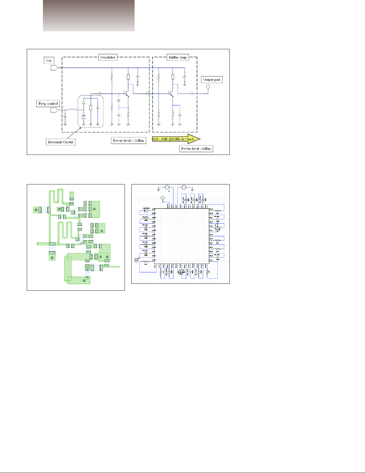
While the use of schematic-based distributed models (Figure 1) offers a quick
method for initial design and optimization,
planar EM simulation eliminates the problems associated with model validity caused by
range restrictions (such as ratios of width to
height) and arbitrary geometries that can be
difficult to model with discrete distributed
models. EM simulation directly models complex trace metals and all their associated parasitic effects such as interconnect coupling. If
the simulation tools support planar EM
parameterization along with circuit-planar
EM hierarchical design, the overall circuit
may be tuned and optimized through manipulation of the physical structure.
Improved EDA tools allow
engineers to easily test and
optimize their designs dur-
ing simulation, before the
expensive and time-con-
suming prototype phase
From January 2004 High Frequency Electronics
Copyright © Summit Technical Media, LLC
58 High Frequency Electronics
High Frequency Design
VCO CHARACTERIZATION
One difficulty when applying EMbased simulations to a free-running
oscillator with a high-Q resonator is
the uncertainty of the nonlinear
oscillation frequency, which is linked
to the resonator circuit. Characterizing the resonator with fine frequency
steps will reduce potential interpolation error at the cost of increased
simulation time. The engineer must
also remember to characterize the
resonator at an appropriate number
of harmonic frequencies if an accurate phase noise simulation is to be
obtained. This increase in frequency
points can detract from the speed
advances offered by today’s more
powerful planar EM tools.
To avoid these problems, Ansoft
Designer offers multiple methods of
planar EM co-simulation that may be
specified by the user. For self-driven
circuits such as an oscillator, the user
may select the fast frequency sweep
option to cover a broad frequency
range using dynamic frequency steps.
The fast frequency sweep option
detects sharp resonances and automatically refines the step size to better capture the changing impedances.
Coarse frequency steps may be
defined to eliminate EM simulations
from being performed in regions outside the range of likely oscillations or
harmonics. For source-driven nonlinear circuits such as amplifiers, the
user may select the discrete frequency co-simulation option so that it is
automatically employed only at the
discrete harmonic frequencies specified by the nonlinear simulation
setup. The desired co-simulation
attribute is easily specified through
the EM component analysis options.
An example of a circuit-planar
EM-based resonator design is shown
in Figures 2 and 3. The hierarchical
approach to this design utilizes a 12port planar EM “sub-design” that is
electrically attached to all surface
mount components, ports, and a DC
source at the design’s top-level. In the
schematic view (Figure 3), the planar
EM component is represented by the
12-port symbol. The fully synchronized layout view shows details of the
resonator’s physical attributes,
including vias and footprints for all
SMT components.
By constructing the resonator
with physical layouts of critical
transmission lines and component
footprints early in the design cycle, it
is possible to ensure that the structure will be realizable. EM co-simulation verifies the structure’s results,
and Ansoft Designer allows circuit
and planar structure hierarchy and
parameter passing so that variables
created by the designer can be used
to define geometries and then be
swept during analysis for parametric
studies. This allows the performance
trade-offs between Q-factor, tuning
range, output power, and phase noise
to be analyzed. In addition, planar
EM simulation may be used to examine the current distribution in the
structure, in order to investigate
undesirable effects such as excessive
coupling between an oscillator and
buffer amplifier (Figure 4).
With the tools in place to properly
characterize the linear network, the
engineer should then consider the
nonlinear aspects of the simulation.
Figure 1 · VCO and buffer amplifier design based on lumped element and
simple transmission line models.
Figure 2 · The VCO layout view,
showing the physical design.
Figure 3 · Schematic view showing
resonator EM structure as multi-port
symbol.
 Loading...