ANPEC APA2822JC-TU Datasheet

Copyright ANPEC Electronics Corp.
Rev. A.2 - Jan., 2001
APA2822
www.anpec.com.tw1
ANPEC reserves the right to make changes to improve reliability or manufacturability without notice, and advise
customers to obtain the latest version of relevant information to verify before placing orders.
Dual Low-Voltage Power Amplifier
Features General Description
Applications
Ordering Information
APA 2822
Handling Code
Temp. Range
Package Code
Package Code
J : PDIP - 8 K : SOP - 8
Temp. Range
C : 0 to +70 C
Handling Code
TU : Tube
°
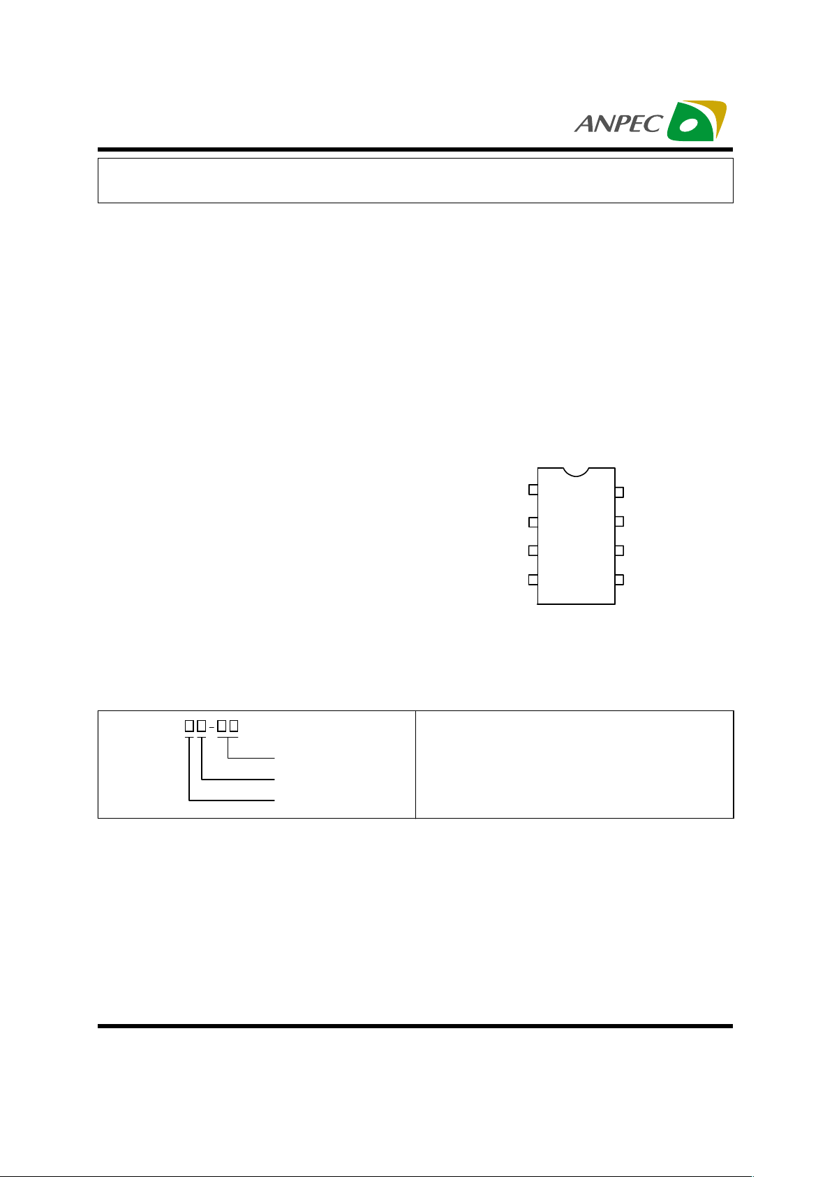
Pin Description
1
2
3
4
Supply Voltage
5
6
7
8
Output (1)
Ground
Output (2)
Input (1)
Input (1)
Input (2)
Input (2)
••
••
• Supply Voltage Down to 1.8V
••
••
• Low Crossover Distortion
••
••
•
Low Quiescent Current
••
••
• Bridge-tied or Stereo(Single-ended) Configura-
tions
••
••
•
Both DIP-8 and SOP-8 packages available
••
••
• Audio Amplifiers
••
••
• Active Speakers
••
••
• Sound Cards
••
••
• Filters
••
••
• Analog Circuit
The APA2822 is a monolithic integrated circuit in 8lead PDIP package. It is intended for use as dual
audio power amplifier in portable cassette players,
active speakers, and radios.

Copyright ANPEC Electronics Corp.
Rev. A.2 - Jan., 2001
APA2822
www.anpec.com.tw2
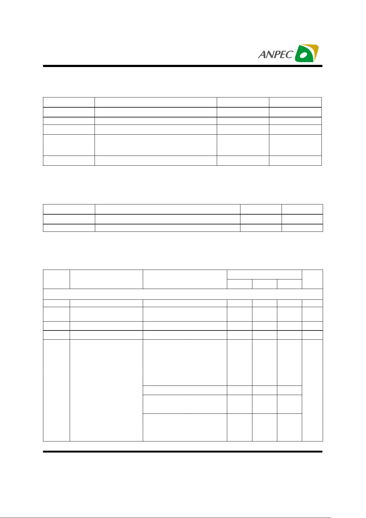
Absolute Maximum Ratings
Thermal Data
Electrical Characteristics
(VS= 6V , TA = 25°C, unless otherwise specified)
Symbol
Parameter Rating Unit
V
CC
Supply Voltage 15 V
I
O
Peak Output Current 1 A
V
I
Input Voltage 15 V
Power Dissipation at T
AMB
= 50°C
P
TOT
at T
CASE
= 50°C
1
1.4
W
T
STG , TJ
Storage and Junction Temperature Range -40 to +150
°
C
Symbol
Parameter Rating Unit
R
TH J-AMB
Thermal Resistance Junction-Ambient Max. 100
°
C/ W
R
TH J-CASE
Thermal Resistance Junction-Pin Max. 70
°
C/ W
APA2822
Symbol Parameter Test Conditions
Min. Typ. Max.
Unit
STEREO (test circuit of Figure 1)
V
S
Supply Voltage 1.8 15 V
V
O
Quiescent Output Voltage
V
S
=3V
2.7
1.2
V
I
D
Quiescent Drain Current 6 mA
I
B
Input Bias Current 100 nA
RL =32
Ω
V
S
= 9V 300
VS = 6V 120
VS = 4.5V
60
VS =3V
20
VS = 2V
5
RL =16
Ω
V
S
= 6V
220
RL =8
Ω
V
S
= 9V 1000
VS = 6V 380
RL =4
Ω
V
S
= 6V
650
VS = 4.5V
320
P
O
Output Power
(f = 1kHz, d = 10%)
V
S
= 3V 110
mW

Copyright ANPEC Electronics Corp.
Rev. A.2 - Jan., 2001
APA2822
www.anpec.com.tw3
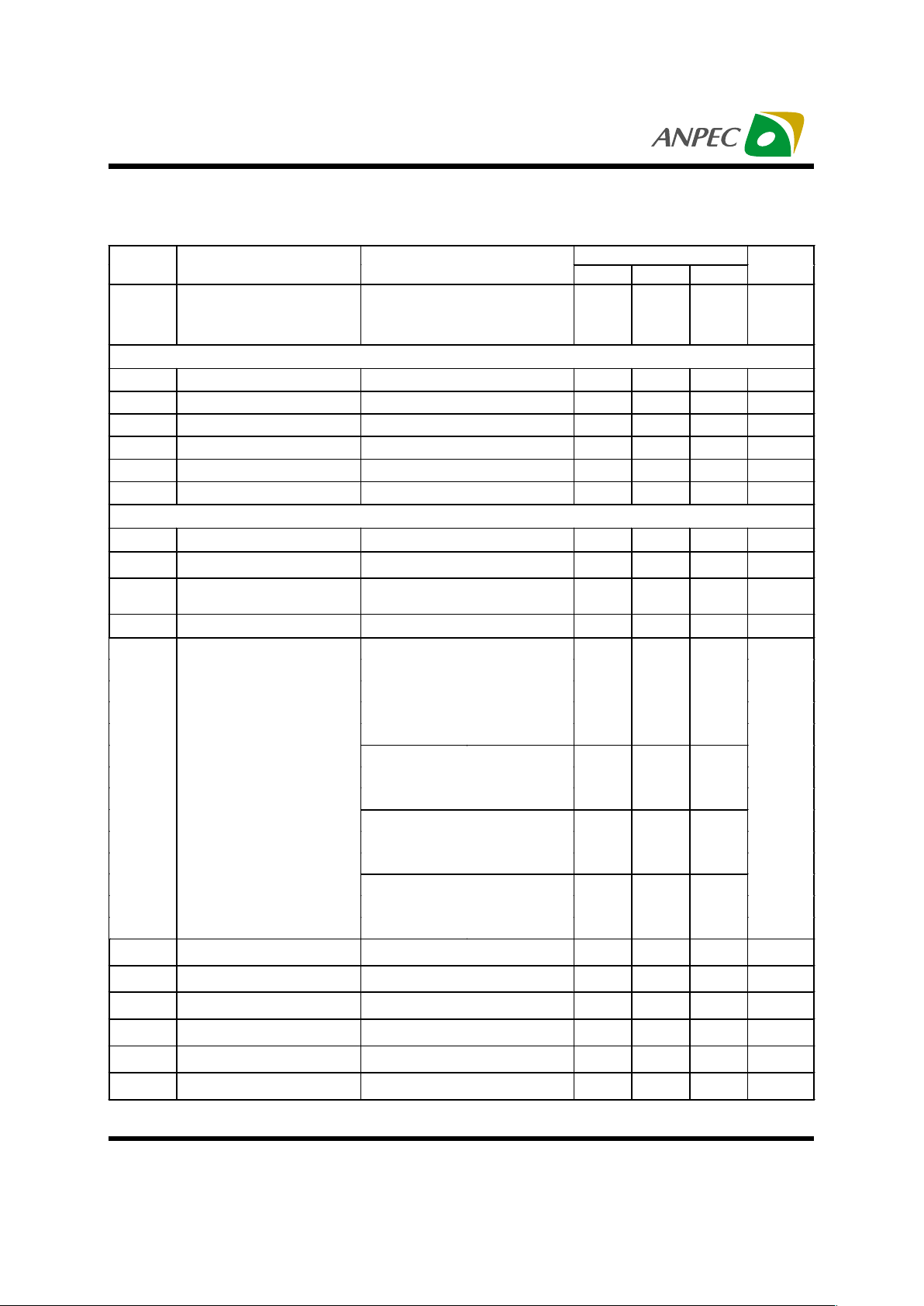
Electrical Characteristics Cont. (V
S
= 6V , TA = 25°C, unless otherwise specified)
APA2822
Symbol Parameter Test Conditions
Min. Typ. Max.
Unit
d
Distortion (f = 1kHz)
R
L
=32
Ω
PO = 40mW
R
L
=16
Ω
PO = 75mW
R
L
= 8
Ω
PO = 150mW
0.2
0.2
0.2
%
STEREO (test circuit of Figure 1)
G
V
Closed Loop Voltage Gain f = 1kHz 39 dB
∆
G
V
Channel Balance
±
1
dB
R
I
Input Resistance f = 1kHz 100
k
Ω
e
N
Total Input Noise
R
S
= 10kΩB = 22Hz to 22kHz
2.5
µ
V
SVR Supply Voltage Rejection
f = 100Hz, C1 = C2 = 100µF
30 dB
C
s
Channel Separation f = 1kHz 50
BRIDGE (test circuit of Figure 2)
V
S
Supply Voltage 1.8 15 V
I
D
Quiescent Drain Current
R
L
=8
Ω
69mA
V
OS
Output Offset Voltage
(between the outputs)
R
L
=8
Ω
±
50
mV
I
B
Input Bias Current 100 nA
V
S
= 9V
1000
V
S
= 6V
400
V
S
= 4.5V
200
VS =3V
65
RL =32
Ω
V
S
= 2V
8
V
S
= 9V
2000
V
S
= 6V
800
RL =16
Ω
V
S
= 3V
120
V
S
= 6V
1350
V
S
= 4.5V
700
RL =8
Ω
V
S
= 3V
220
V
S
= 4.5V
1000
V
S
= 3V
350
P
O
Output Power
(f = 1kHz, d = 10%)
R
L
=4
Ω
V
S
= 2V
80
mW
d
Distortion P
O
= 0.5W, RL =8Ω, f = 1kHz
0.2 %
G
V
Closed Loop Voltage Gain f = 1kHz
39 dB
R
J
Input Resistance f = 1kHz
100 k
Ω
e
N
Total Input Noise RS =10kΩ, B = 22Hz to 22kHz
3
µ
V
SVR
Supply Voltage Rejection f = 100Hz
30
dB
B
Power Bandwidth (-3dB) R
L
=8Ω, PO = 1W
120 kHz
 Loading...