

Class AB Stereo Headphone Driver
Copyright ANPEC Electronics Corp.
Rev. B.3 - Jun., 2003
APA2308
www.anpec.com.tw1
ANPEC reserves the right to make changes to improve reliability or manufacturability without notice, and advise
customers to obtain the latest version of relevant information to verify before placing orders.
Features
Ordering and Marking Information
The APA2308 is an integrated class AB stereo headphone driver contained in an SO-8, a DIP-8 or a
TSSOP-8 plastic package. The APA2308 is capable
of delivering 280mW of max. Output power to an 8Ω
load or 110mW to a 32Ω load with less than 10%
(THD+N) from a 5V power supply. The device is fabricated in a CMOS process and has been primarily
developed for portable digital audio applications .
Applications
• Portable Digital Audio
Gereral Description
••
••
•
Operating Voltage
Single Supply 3V to 6V
Dual Supply ±1.5V to ± 3.0V
••
••
•
High Signal-to-Noise Ratio 100dB
••
••
•
Low Distortion -65dB
••
••
•
Large Output Voltage Swing
••
••
• Excellent Power Supply Ripple Rejection
••
••
• Low Power Consumption
••
••
• Short-circuit Elimination
••
••
• Wide Temperature Range
••
••
• No Switch ON/OFF Clicks
••
••
• Available in 8 pin SOP ,DIP or TSSOP Package
APA2308
Package Code
J : P DIP - 8 K : SOP - 8
O : T SSO P - 8
Temp. Range
I : - 40 to 85 C
Handling Code
TU : Tube TR : Tape & Reel
°
Handling Code
Temp. Range
Package Code
APA2308 J : APA2308
XXXXX
XXXXX - Date Code
APA2308 K :
APA2308
XXXXX
XXXXX - Date Code
APA2308 O :
APA2308
XXXXX
XXXXX - Date Code
Copyright ANPEC Electronics Corp.
Rev. B.3 - Jun., 2003
APA2308
www.anpec.com.tw2
Thermal Characteristics
Absolute Maximum Ratings
Electrical Characteristics
VDD=5V , VSS=0V , TA=25°C , fi=1kHz , RL=32Ω ( unless otherwise noted)
Note : *1. Human body model : C=100pF , R=1500Ω , 3 positive pulses plus 3 negative pulses
Symbol Parameter Value Unit
R
THJA
Thermal Resistance from Junction to Ambient in Free Air
DIP-8
SO-8
109
210
K/W
K/W
Symbol Parameter Rating Unit
V
DD
Supply Voltage 7 V
T
SC(O)
Output Short-circuit Duration,at TA=25°C,PTOT=1W 20 S
T
A
Operating Ambient Temperature range -40 to 85 °C
T
J
Maximum Junction Temperature 150 °C
T
STG
Storage Temperature Range -65 to +150 °C
T
S
Soldering Temperature , 10 seconds 260 °C
V
ESD
Electrostatic Discharge -3000 to 3000
*1
V
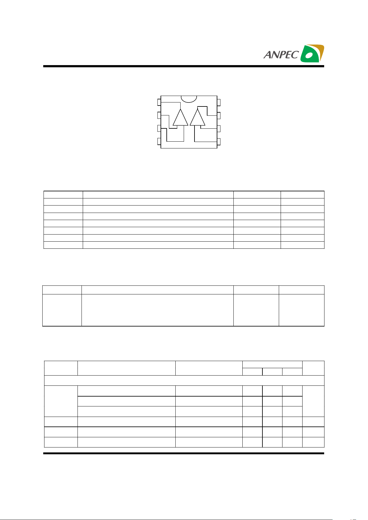
Block Diagram
APA2308
1
2
3
4
5
6
7
8
Out A
Inverting Input A
Non-inverting Input A
Non-inverting Input B
Out B
Inverting Input B
--+
+
V
SS
V
DD
APA2308
Symbol Parameter Test Condition
Min. Typ. Max
Unit
Supply
Supply Voltage
Single 3.0 5.0 6.0
V
DD
Dual ±1.5 ±2.5 ±3.0
V
V
SS
Negative Supply Voltage -1.5 -2.5 -3.0 V
I
DD
Supply Current No Load 2.5 5 MA
P
TOT
Total Power Dissipation No Load 12.5 25 mW
Copyright ANPEC Electronics Corp.
Rev. B.3 - Jun., 2003
APA2308
www.anpec.com.tw3
APA2308
Symbol Parameter Test Condition
Min. Typ. Max
Unit
DC Characteristics
V
I(OS)
Input Offset Voltage 5 MV
I
BIAS
Input Bias Current 10 PA
V
CM
Common Mode Voltage 0 3.5 V
G
V
Open-loop Voltage Gain
R
L
=5k
Ω
75 dB
I
O
Max. Output Current (THD+N)/S<0.1% 140 MA
R
O
Output Resistance 0.25
Ω
AC Characteristics
RL=32Ω
*
1
0.25 4.75V
O
Output Voltage Swing
R
L
=16
Ω*
1
0.5 4.5
V
PSRR Power Supply Rejection Ratio Fi=100Hz
V
RIPPLE(P -P)
=100mV
65 dB
\
CS
Channel Separation
R
L
=32
Ω
95 dB
C
L
Load Capacitance 200 pF
-65 -60 dB(THD+N)/S Total Harmonic Distortion Plus
Noise to Signal Ratio
R
L
=32Ω*
2
0.05 0.1
S/N Signal to Noise Ratio 90 100 dB
F
G
Unity G ain Freque nc y
R
L
=5kΩ
5MHz
P
O
Max. Output Power
(THD+N)/S<0.1%
84
mW
C
I
Input Capacitance 3 pF
B Power Bandwidth Unity Gain Inverting 20 kHz
Notes *1 : Values are proportional to VDD ; (THD+N)/S < 0.1%
*2 : V
DD
=5.0V ; V
O(P-P)
=3.5V (at 0 dB)
Electrical Characteristics Cont.
VDD=5V, VSS=0V, TA=25°C, fi=1kHz, RL=32Ω ( unless otherwise noted)
Copyright ANPEC Electronics Corp.
Rev. B.3 - Jun., 2003
APA2308
www.anpec.com.tw4
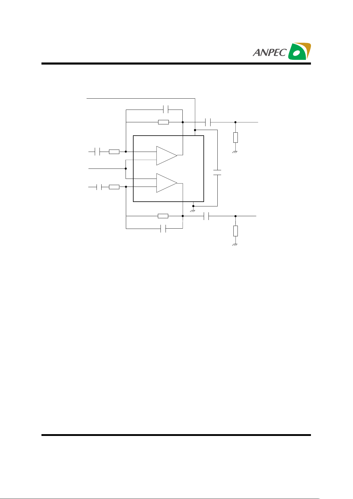
Test And Application Circuits
220pF
1
2
3
4
6
7
8
+
-
+
15k
Ω
15k
Ω
15k
Ω
15k
Ω
V
INA
V
INB
R
L
R
L
220µF
100
µ
F
V
DD
V
OUTA
V
OUTB
220µF
2.2
µ
F
220pF
5
2.2µF
APA2308
V
REF
typ.1/2V
DD

Copyright ANPEC Electronics Corp.
Rev. B.3 - Jun., 2003
APA2308
www.anpec.com.tw5
Typical Characteristics
Total Harmonic Distortion Plus Noise-toSignal Ratio as a Function of Input Frequency
Output Power as a Function of Supply
Voltage
Crosstalk as a Function of Input
Frequency
Open Loop Gain as a Function of Input
Frequency
-120
-100
-80
100 1k
RL=5k
Ω
RL=32
Ω
RL=16
Ω
RL=8
Ω
10k
No load
+60
+20
+40
+80
1k 10k
100k 1M
RL=32
Ω
Frequency (Hz)
(THD+N) / S (dB)
VDD (Vrms)
P
O
(mW)
Frequency (Hz)
Xtalk
Frequency (Hz)
Gv (dB)
2
5
10
20
100
200
5.52.5 3.5
4.5
RL=8
Ω
RL=16
Ω
RL=32
Ω
-100
-80
-60
100 1k 10k
RL=8
Ω
RL=16
Ω
RL=32
Ω
RL=5k
Ω
po=50mW
po=50mW
po=50mW
V
o(PP)
=3.5V

Copyright ANPEC Electronics Corp.
Rev. B.3 - Jun., 2003
APA2308
www.anpec.com.tw6
Typical Characteristics Cont.
Total Harmonic Distortion Plus Noise-to-
Signal Ratio as a Function of output
Voltage
-90
-80
-70
-60
-50
-40
2100m 500m 1
RL=8
Ω
RL=16
Ω
RL=32
Ω
RL=5K
Ω
Vo (Vrms)
(THD+N) / S (dB)

Copyright ANPEC Electronics Corp.
Rev. B.3 - Jun., 2003
APA2308
www.anpec.com.tw7
Packaging Information
1
D
E1
A2
A1
A
L
e2
e 3
e 1
E
E3
1
PDIP-8 pin ( Reference JEDEC Registration MS-001)
Millimeters InchesDim
Min. Max. Min. Max.
A
5.33 0.210
A1
0.38 0.015
A2
2.92 3.68 0.115 0.145
D
9.02 10.16 0.355 0.400
e1
2.54BSC 0.100BSC
e2
0.36 0.56 0.014 0.022
e3
1.14 1.78 0.045 0.070
E
7.62 BSC 0.300 BSC
E1
6.10 7.11 0.240 0.280
E3
10.92 0.430
L
2.92 3.81 0.115 0.150
φ
115
°
15
°

Copyright ANPEC Electronics Corp.
Rev. B.3 - Jun., 2003
APA2308
www.anpec.com.tw8
Packaging Information
Millimeters Inches
Dim
Min. Max. Min. Max.
A 1.35 1.75 0.053 0.069
A1 0.10 0.25 0.004 0.010
D 4.80 5.00 0.189 0.197
E 3.80 4.00 0.150 0.157
H 5.80 6.20 0.228 0.244
L 0.40 1.27 0.016 0.050
e1 0.33 0.51 0.013 0.020
e2 1.27BSC 0.50BSC
φ
18
°
8
°
HE
e1 e2
0.015X45
D
A
A1
0.004max.
1
L
SOP-8 pin ( Reference JEDEC Registration MS-012)

Copyright ANPEC Electronics Corp.
Rev. B.3 - Jun., 2003
APA2308
www.anpec.com.tw9
Packaging Information
Millimeters Inches
Dim
Min. Max. Min. Max.
A 1.2 0.047
A1 0.00 0.15 0.000 0.006
A2 0.80 1.05 0.031 0.041
b 0.19 0.30 0.007 0.012
D 2.9 3.1 0.114 0.122
e 0.65 BSC 0.026 BSC
E 6.40 BSC 0.252 BSC
E1 4.30 4.50 0.169 0.177
L 0.45 0.75 0.018 0.030
L1 1.0 REF 0.039REF
R 0.09 0.004
R1 0.09 0.004
S 0.2 0.008
φ
10
°
8
°
0
°
8
°
φ
212
°
REF 12° REF
φ
312
°
REF 12° REF
L
(L1)
(3)
S
(2)
0.25
GAUGE
PLANE
1
b
D
e
2 x E / 2
8
12
e/2
E1 E
7
A1
A2
A
TSSOP-8

Copyright ANPEC Electronics Corp.
Rev. B.3 - Jun., 2003
APA2308
www.anpec.com.tw10
Physical Specifications
Reference JEDEC Standard J-STD-020A APRIL 1999
Reflow Condition (IR/Convection or VPR Reflow)
Pre-heat temperature
183 C
Peak temperature
Time
°
temperature
Classification Reflow Profiles
Convection or IR/
Convection
VPR
Average ramp-up rate(183°C to Peak) 3°C/second max. 10 °C /second max.
Preheat temperature 125 ± 25°C)
120 seconds max
Temperature maintained above 183°C
60 – 150 seconds
Time within 5°C of actual peak temperature
10 –20 seconds 60 seconds
Peak temperature range
220 +5/-0°C or 235 +5/-0°C 215-219°C or 235 +5/-0°C
Ramp-down rate
6 °C /second max. 10 °C /second max.
Time 25°C to peak temperature
6 minutes max.
Package Reflow Conditions
pkg. thickness
≥≥≥≥
2.5mm
and all bgas
pkg. thickness < 2.5mm and
pkg. volume
≥≥≥≥
350 mm³
pkg. thickness < 2.5mm and pkg.
volume < 350mm³
Convection 220 +5/-0 °C Convection 235 +5/-0 °C
VPR 215-219 °C VPR 235 +5/-0 °C
IR/Convection 220 +5/-0 °C IR/Convection 235 +5/-0 °C
Terminal Material Solder-Plated Copper (Solder Material : 90/10 or 63/37 SnPb)
Lead Solderability Meets EIA Specification RSI86-91, ANSI/J-STD-002 Category 3.

Copyright ANPEC Electronics Corp.
Rev. B.3 - Jun., 2003
APA2308
www.anpec.com.tw11
Test item Method Description
SOLDERABILITY MIL-STD-883D-2003
245
°
C , 5 SEC
HOLT MIL-STD-883D-1005.7
1000 Hrs Bias @ 125
°
C
PCT JESD-22-B, A102
168 Hrs, 100 % RH , 121
°
C
TST MIL-STD-883D-1011.9
-65
°
C ~ 150°C , 200 Cycles
ESD MIL-STD-883D-3015.7 VHBM > 2KV, VMM > 200V
Latch-Up JESD 78 10ms , Itr > 100mA
Reliability test Program
Carrier Tape & Reel Dimensions
A
J
B
T2
T1
C
t
Ao
E
W
Po
P
Ko
Bo
D1
D
F
P1
Application
A B C
J T1 T2 W P E
330 ± 1 62 +1.5
12.75+
0.15
2 ± 0.5 12.4 ± 0.2 2 ± 0.2 12± 0. 3 8± 0.1 1.75±0.1
F D
D1 Po P1 Ao Bo Ko tSOP- 8
5.5± 1 1.55 +0.1 1.55+ 0.25 4.0 ± 0.1 2.0 ± 0.1 6.4 ± 0.1 5.2± 0. 1 2.1± 0.1 0.3±0.013
Application
A B C
J T1 T2 W P E
330 ± 1 62 +1.5
12.75+
0.15
2 + 0.5 12.4 ± 0.2 2 ± 0.2 12± 0. 3 8± 0.1 1.75±0.1
F D
D1 Po P1 Ao Bo Ko tTSSOP-8
5.5 ± 0. 1 1.5 + 0.1 1.5 + 0.1 4.0 ± 0.1 2.0 ± 0.1 7.0 ± 0.1 3.6 ± 0.3 1.6 ± 0.1 0.3±0.013
(mm)

Copyright ANPEC Electronics Corp.
Rev. B.3 - Jun., 2003
APA2308
www.anpec.com.tw12
Cover Tape Dimensions
Application Carrier Width Cover Tape Width Devices Per Reel
SOP- 8
12 9.3 2500
TSSOP- 8
12 9.3 2500
Customer Service
Anpec Electronics Corp.
Head Office :
5F, No. 2 Li-Hsin Road, SBIP,
Hsin-Chu, Taiwan, R.O.C.
Tel : 886-3-5642000
Fax : 886-3-5642050
Taipei Branch :
7F, No. 137, Lane 235, Pac Chiao Rd.,
Hsin Tien City, Taipei Hsien, Taiwan, R. O. C.
Tel : 886-2-89191368
Fax : 886-2-89191369
 Loading...