

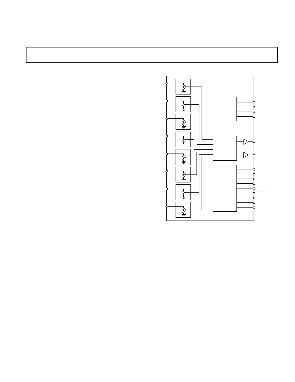
Digitally Controlled
V
IN1
DCA
V
IN2
DCA
V
IN3
DCA
V
IN4
DCA
V
IN5
DCA
V
IN
6
DCA
V
IN
7
DCA
V
IN8
DCA
OUTPUT
SWITCHING
NETWORK
VOLTAGE
REFERENCE
GENERATOR
V
CC
V
EE
ACOM
AGND
V
OUTL
V
OUTR
SHIFT
REGISTER
AND
ADDRESS
DECODER
SYSTEM MUTE
DATA OUT
CLK
DATA
LD
WRITE
DGND
V
DD
V
SS
SSM2163
DCA: DIGITALLY CONTROLLED ATTENUATOR
a
FEATURES
Each of 8 Inputs Can Be Assigned to Either or Both
Outputs
Voltage Inputs and Outputs – No Need For External
Amplifiers
Each Input Provides 63 dB of Attenuation in 1 dB Steps,
Plus Mute
–82 dBu Signal-to-Noise Ratio (0 dBu = 0.775 V
+10 dBu of Headroom
0.007% THD+N (Unity Gain, @ 1 kHz, 0 dBu)
Power-Up/System Mute Feature
Industry-Standard 3-Wire Serial Interface
Data Out Terminal Permits Daisy Chaining of Multiple
SSM2163s
Single or Dual Supply Operation
28-Pin Plastic DIP and SOIC Package
APPLICATIONS
Multimedia System Mixing
Audio Mixing Consoles
Broadcast Equipment
Intercom/Paging Systems
Musical Instruments
rms)
8 3 2 Audio Mixer
SSM2163
SIMPLIFIED BLOCK DIAGRAM
GENERAL DESCRIPTION
The SSM2163 provides eight audio inputs, each of which can
be mixed under digital control to a stereo output. Each input
channel can be attenuated up to 63 dB in 1 dB intervals, plus
fully muted. Additionally, any input can be assigned to either or
both outputs. A standard 3-wire serial interface is employed,
plus a Data Out terminal to facilitate daisy chaining of multiple
mixer ICs. No external components are required for normal
operation.
Excellent audio performance is attained. The SSM2163 has a
signal-to-noise ratio of –82 dBu (0 dBu = 0.775 V rms), with
10 dBu of headroom resulting in total dynamic range of 92 dBu.
The SSM2163 can be operated from single (+5 V to +14 V) or
dual (±4 V to ±7 V) supplies, and is housed in 28-pin plastic
DIP and SOIC packages.
The SSM2163 is an ideal companion product to the Analog
Devices family of stereo codecs in high performance multimedia systems requiring mixing of multiple signals.
Total harmonic distortion plus noise is 0.007% at 1 kHz with all
levels set at unity gain.
REV. 0
Information furnished by Analog Devices is believed to be accurate and
reliable. However, no responsibility is assumed by Analog Devices for its
use, nor for any infringements of patents or other rights of third parties
which may result from its use. No license is granted by implication or
otherwise under any patent or patent rights of Analog Devices.
© Analog Devices, Inc., 1995
One Technology Way, P.O. Box 9106, Norwood, MA 02062-9106, U.S.A.
Tel: 617/329-4700 Fax: 617/326-8703

SSM2163–SPECIFICATIONS
(VS = 65 V, AV = 0 dB, VIN = 0 dBu = 0.775 V rms, f
ELECTRICAL SPECIFICATIONS
–408C < TA < +858C, unless otherwise noted. Typical specifications apply at TA = +258C.)
Parameter Conditions Min Typ Max Units
AUDIO PERFORMANCE
Noise V
= GND, 20 kHz Bandwidth –82 dBu
IN
Headroom Clip Point = 1% THD+N +10 dBu
Total Harmonic Distortion Plus Noise 2nd and 3rd Harmonics Only
A
= 0 dB 0.007 0.03 %
V
A
= –20 dB 0.02 %
V
AV = 0 dB, VS = +5 V, Single Supply 0.035 %
ANALOG INPUT
Input Impedance 71015kΩ
VOLUME CONTROL
Step Size 1.0 dB
Gain Error Relative to Same Channel
0 dB Attenuation 0.1 1.0 dB
–20 dB Attenuation 0.1 dB
–40 dB Attenuation 0.25
Gain Match Error Channel-to-Channel; Same Level Setting
0 dB Attenuation 0.01 dB
–20 dB Attenuation 0.05 dB
–40 dB 0.4 dB
Mute Attenuation 64 dB
AUDIO
= 1 kHz, f
= 250 kHz, RL = 100 kV,
CLK
ANALOG OUTPUT
Output Impedance 15 Ω
Output Current 500 µA
Minimum Resistive Load THD = 1% 4 kΩ
Maximum Capacitive Drive 5000 pF
Offset Voltage Channel Muted 50 mV
CONTROL SECTION
Logic Input LO 0.8 V
Logic Input HI 2.0 V
Logic Input Current Logic LO or HI 1 µA
Logic Out LO I
Logic Out HI I
= 0.2 mA 0.4 V
OUT
= 0.2 mA 2.4 V
OUT
Timing Characteristics See Timing Diagram
REFERENCE (ACOM)
Output Voltage V
= +10 V (Single Supply) 4.7 5.0 5.3 V
S
Output Impedance 10 Ω
Load Regulation –0.5 mA ≤ IL ≤ +0.5 mA (Single Supply) 0.2 %
POWER SUPPLIES
Supply Voltage Range Dual Supply ±4 ±7V
Single Supply +5 +14 V
Supply Current V
= +10 V (Single Supply) 8 15 mA
S
Power Supply Rejection Ratio Delta Gain 0.005 dB/V
Specifications subject to change without notice.
–2–
REV. 0
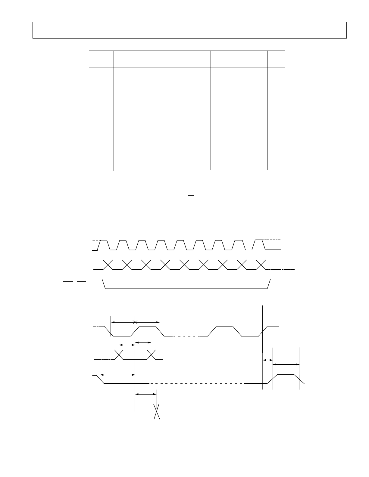
Timing Description
Timing
Symbol Description Min Typ Max Units
SSM2163
t
t
t
t
t
t
t
t
t
t
t
CL
CH
DS
DH
CW
WC
LW
WL
L
W3
PD
Input Clock Pulse Width 50 ns
Input Clock Pulse Width 50 ns
Data Setup Time 25 ns
Data Hold Time 35 ns
Positive CLK Edge to End of Write 25 ns
Write to Clock Setup Time 35 ns
End of Load Pulse to Next Write 20 ns
End of Write to Start of Load 20 ns
Load Pulse Width 250 ns
Load Pulse Width (3-Wire Mode) 250 ns
Propagation Delay from Rising 10 80 160 ns
Clock to SDO Transition
(RL = 220 kΩ, CL = 20 pF)
NOTES
1. An idle HI (CLK-HI) or idle LO (CLK-LO) clock may be used. Data is latched on the positive
edge.
2. For SPI or microwire three-wire bus operation, tie LD to WRITE and use WRITE pulse to drive
both pins. (This generates an automatic internal LD signal.)
3. If an idle HI clock is used, tCW and tWL are measured from the final negative transition to the idle
state.
4. The first data byte selects an address (MSB HI), and subsequent MSB LO states set gain levels. Refer to the Address/Data Decoding Truth Table.
5. Data must be sent MSB first.
1
CLK
0
DATA
WRITE & LOAD
CLK
DATA
WRITE & LOAD
SDO
1
0
1
0
1
0
1
0
1
0
1
0
D7 D6 D5 D4 D3 D2 D1 D0
t
CL
t
DS
t
WC
t
CH
t
DH
t
PD
t
CW
t
W3
REV. 0
Figure 1. Three-Wire Mode Timing Diagram
–3–
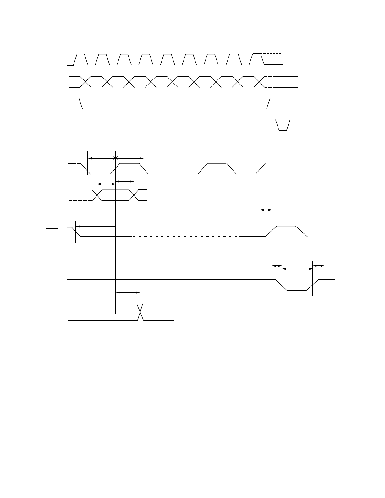
SSM2163
CLK
DATA
WRITE
LD
1
0
1
D7 D6 D5 D4 D3 D2 D1 D0
0
1
0
1
0
CLK
DATA
WRITE
LOAD
SDO
t
CL
1
0
t
DS
1
0
t
1
0
1
0
1
0
WC
t
CH
t
DH
t
CW
t
WL
t
PD
t
t
L
LW
Figure 2. Four-Wire Mode Timing Diagram
–4–
REV. 0
SSM2163
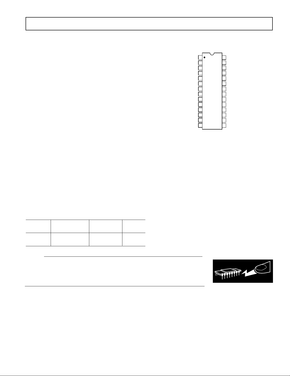
14
13
12
11
17
16
15
20
19
18
10
9
8
1
2
3
4
7
6
5
28
27
26
25
24
23
22
21
TOP VIEW
(Not to Scale)
SSM2163
DGND
WRITE
CLK
DATA IN
SYSTEM MUTE
V
SS
DATA OUT
V
DD
V
IN2
NC (SHIELD)
LD
V
IN1
NC (SHIELD)
V
IN3
NC (SHIELD)
V
IN5
V
CC
NC (SHIELD)
V
IN4
NC (SHIELD)
V
IN7
V
EE
ACOM
V
OUTL
V
IN6
V
OUTR
V
IN8
AGND
ABSOLUTE MAXIMUM RATINGS
1
Supply Voltage
Dual Supply . . . . . . . . . . . . . . . . . . . . . . . . . . . . . . . . . ±8 V
Single Supply . . . . . . . . . . . . . . . . . . . . . . . . . . . . . . . +16 V
Analog Input Voltage . . . . . . . . . . . . . . . . . . . . . . . . . . . . . ±V
Logic Input Voltage . . . . . . . . . . . . . . . . . . . . . . . . . . . . . . ±V
S
S
Output Current . . . . . . . . . . . . . . . . . . . . . . . . . . . . . . . . 5 mA
Operating Temperature Range . . . . . . . . . . . . –40°C to +85°C
Storage Temperature . . . . . . . . . . . . . . . . . . –65°C to +150°C
Junction Temperature (T
) . . . . . . . . . . . . . . . . . . . . . +150°C
J
Lead Temperature (Soldering, 60 sec) . . . . . . . . . . . . . +300°C
THERMAL CHARACTERISTICS
Thermal Resistance
2
28-Pin Plastic DIP (SSM2163P)
θ
. . . . . . . . . . . . . . . . . . . . . . . . . . . . . . . . . . . . . 48°C/W
JA
θ
. . . . . . . . . . . . . . . . . . . . . . . . . . . . . . . . . . . . 22°C/W
JC
28-Pin SOIC (SSM2163S)
θ
. . . . . . . . . . . . . . . . . . . . . . . . . . . . . . . . . . . . . 68°C/W
JA
θ
. . . . . . . . . . . . . . . . . . . . . . . . . . . . . . . . . . . . 20°C/W
JC
TRANSISTOR COUNT
Number of Transistors . . . . . . . . . . . . . . . . . . 1711 MOSFETs
447 BJTs
ESD RATINGS
883 (Human Body) Model . . . . . . . . . . . . . . . . . . . . . .1000 V
NOTES
1
Stresses above those listed under “Absolute Maximum Ratings” may cause
permanent damage to the device. This is a stress rating only and functional
operation of the device at these or any other conditions above those indicated in the
operation section of this specification is not implied. Exposure to absolute maximum rating conditions for extended periods may affect device reliability.
2
θJA is specified for worst-case conditions, i.e., θJA is specified for device in socket
for P-DIP and device soldered in circuit board for SOIC package.
PIN CONFIGURATIONS
Epoxy Plastic DIP (P-Suffix)
and SOIC (S-Suffix)
ORDERING GUIDE
Temperature Package Package
Model Range Description Option
SSM2163P –40°C to +85°C Plastic DIP N-28
SSM2163S –40 °C to +85°C SOIC R-28
CAUTION
ESD (electrostatic discharge) sensitive device. Electrostatic charges as high as 4000 V readily
accumulate on the human body and test equipment and can discharge without detection.
Although the SSM2163 features proprietary ESD protection circuitry, permanent damage may
occur on devices subjected to high energy electrostatic discharges. Therefore, proper ESD
precautions are recommended to avoid performance degradation or loss of functionality.
–5–
REV. 0
WARNING!
ESD SENSITIVE DEVICE
 Loading...