

Precision Picoampere Input Current
FEATURES
Low offset voltage: 75 μV maximum
Low offset voltage drift: 1.0 μV/°C maximum
Very low bias current
25°C: 150 pA maximum
−40°C to +85°C: 300 pA maximum
Very high open-loop gain: 2000 V/mV minimum
Low supply current (per amplifier): 625 μA maximum
Operates from ±2 V to ±20 V supplies
High common-mode rejection: 114 dB minimum
APPLICATIONS
Strain gage and bridge amplifiers
High stability thermocouple amplifiers
Instrumentation amplifiers
Photocurrent monitors
High gain linearity amplifiers
Long-term integrators/filters
Sample-and-hold amplifiers
Peak detectors
Logarithmic amplifiers
Battery-powered systems
GENERAL DESCRIPTION
The OP497 is a quad op amp with precision performance in
the space-saving, industry standard 16-lead SOlC package.
Its combination of exceptional precision with low power and
extremely low input bias current makes the quad OP497 useful
in a wide variety of applications.
Precision performance of the OP497 includes very low offset
(<50 µV) and low drift (<0.5 µV/°C). Open-loop gain exceeds
2000 V/mV ensuring high linearity in every application. Errors
due to common-mode signals are eliminated by its commonmode rejection of >120 dB. The OP497 has a power supply
rejection of >120 dB which minimizes offset voltage changes
experienced in battery-powered systems. The supply current
of the OP497 is <625 µA per amplifier, and it can operate with
supply voltages as low as ±2 V.
The OP497 uses a superbeta input stage with bias current
cancellation to maintain picoamp bias currents at all temperatures.
This is in contrast to FET input op amps whose bias currents
start in the picoamp range at 25°C but double for every 10°C
rise in temperature to reach the nanoamp range above 85°C.
The input bias current of the OP497 is <100 pA at 25°C.
Quad Operational Amplifier
OP497
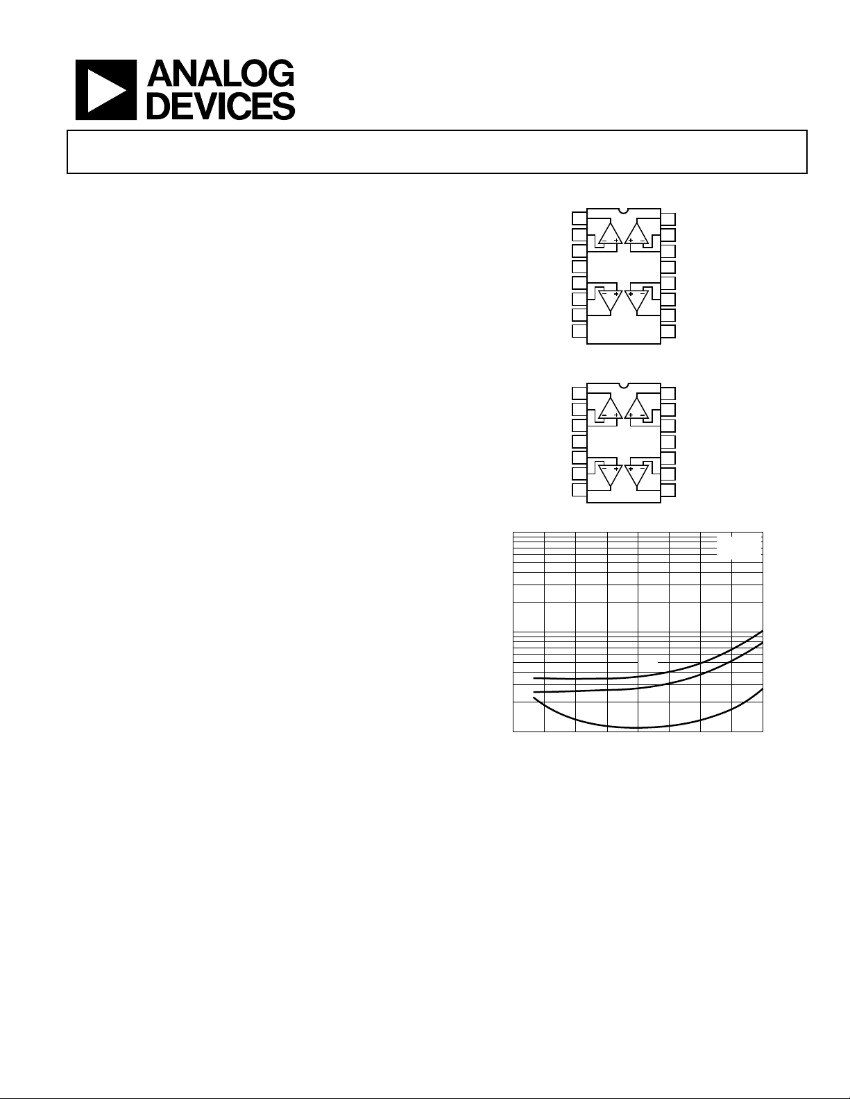
PIN CONNECTIONS
1
OUT A
2
–IN A
3
+IN A
4
V+
+IN B
–IN B
OUT B
NC
OP497
5
6
7
8
NC = NO CONNECT
Figure 1. 16-Lead Wide Body SOIC (RW-16)
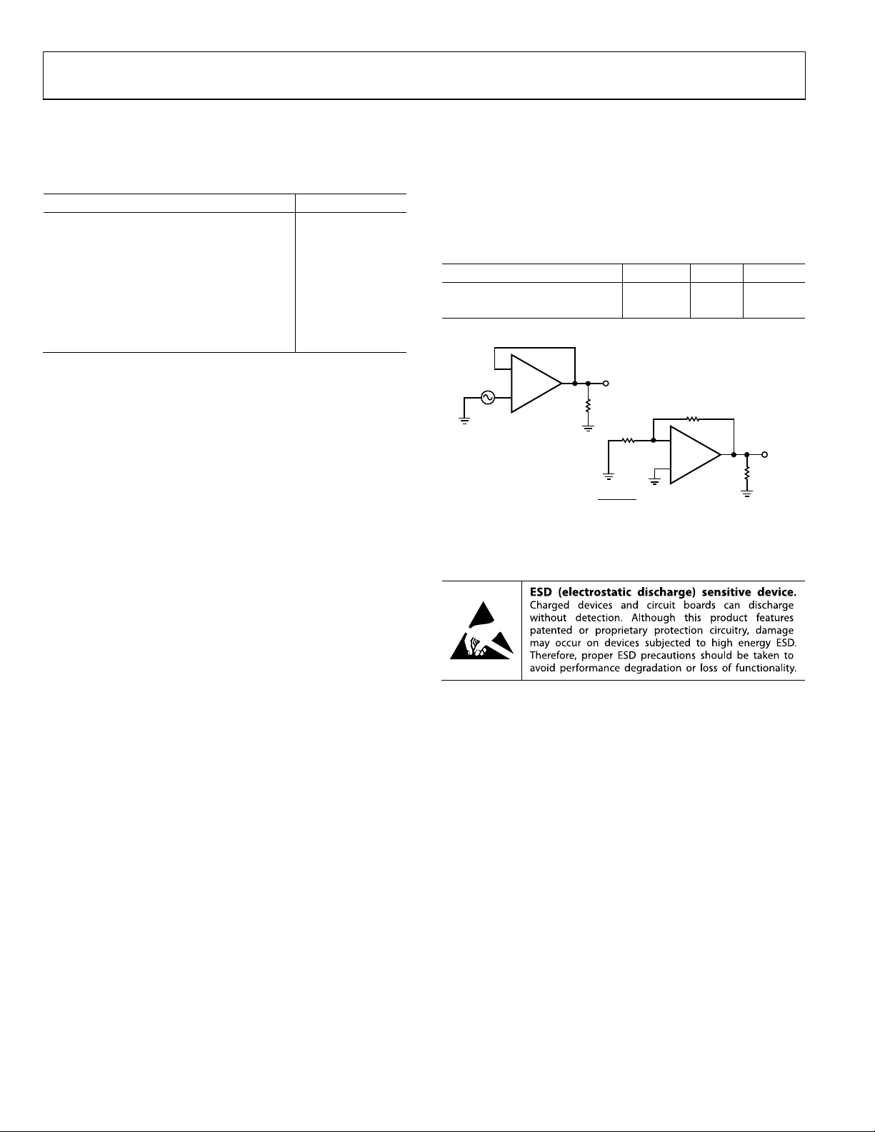
1
OUT A
2
–IN A
3
+IN A
4
V+
+IN B
–IN B
OUT B
OP497
5
6
7
Figure 2. 14-Lead PDIP (N-14)
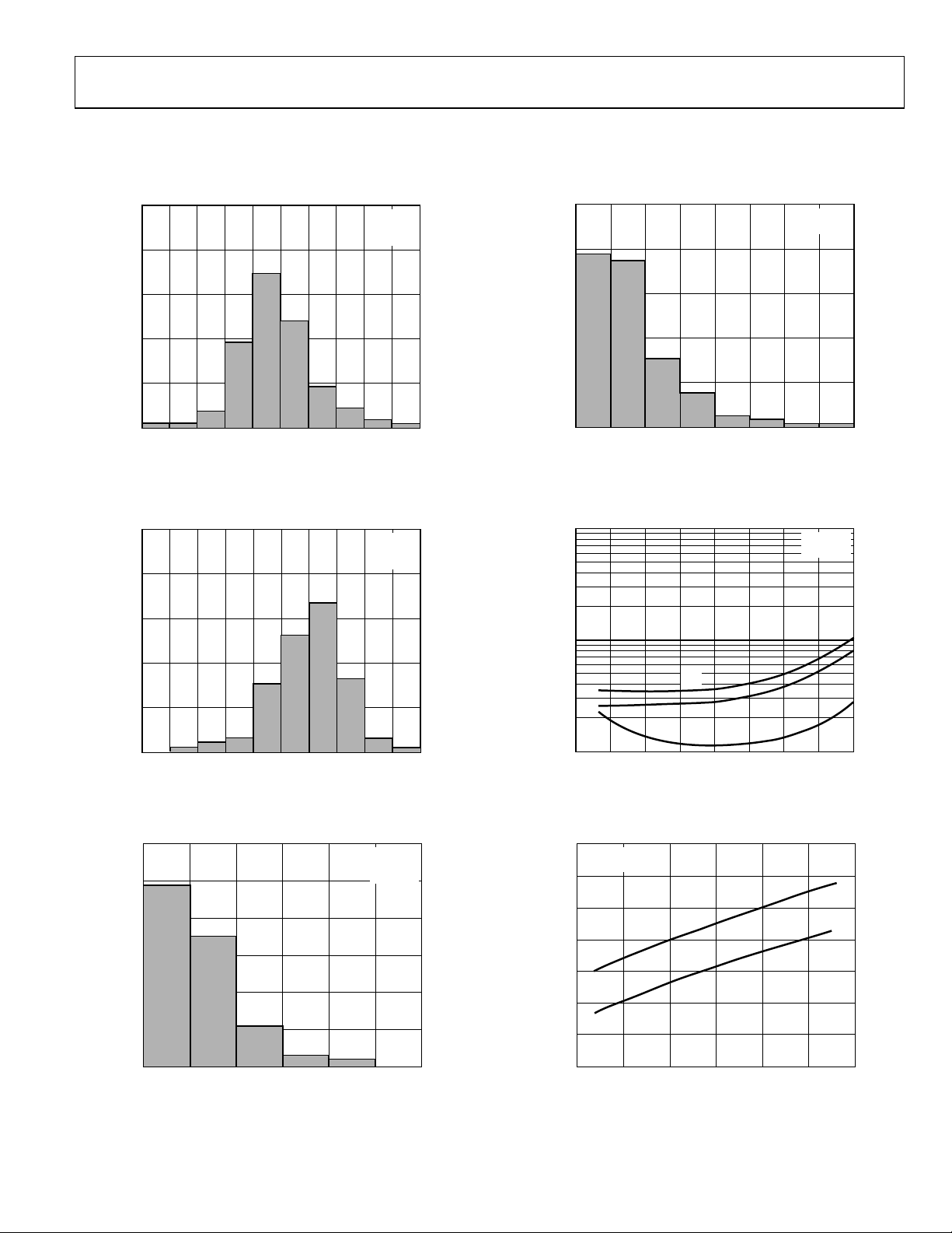
1k
100
INPUT CURRENT (pA)
10
–75 –50 –25 0 25 50 75 100 125
TEMPERATURE (°C)
Figure 3. Input Bias, Offset Current vs. Temperature
Combining precision, low power, and low bias current, the OP497
is ideal for a number of applications, including instrumentation
amplifiers, log amplifiers, photodiode preamplifiers, and longterm integrators. For a single device, see the OP97 data sheet,
and for a dual device, see the OP297 data sheet.
16
OUT D
15
–IN D
14
+IN D
13
V–
12
+IN C
11
–IN C
10
OUT C
9
NC
00309-001
14
OUT D
13
–IN D
12
+IN D
11
V–
10
+IN C
9
–IN C
8
OUT C
00309-002
VS = ±15V
= 0V
V
CM
–I
B
+I
B
I
OS
0309-003
Rev. E
Information furnished by Analog Devices is believed to be accurate and reliable. However, no
responsibility is assumed by Analog Devices for its use, nor for any infringements of patents or other
rights of third parties that may result from its use. Specifications subject to change without notice. No
license is granted by implication or otherwise under any patent or patent rights of Analog Devices.
Trademarks and registered trademarks are the property of their respective owners.
One Technology Way, P.O. Box 9106, Norwood, MA 02062-9106, U.S.A.
Tel: 781.329.4700 www.analog.com
Fax: 781.461.3113 ©1991–2009 Analog Devices, Inc. All rights reserved.

OP497
TABLE OF CONTENTS
Features .............................................................................................. 1
Applications ....................................................................................... 1
General Description ......................................................................... 1
Pin Connections ............................................................................... 1
Revision History ............................................................................... 2
Specifications ..................................................................................... 3
Absolute Maximum Ratings ............................................................ 4
Thermal Resistance ...................................................................... 4
ESD Caution .................................................................................. 4
Typical Performance Characteristics ............................................. 5
Applications Information .............................................................. 10
REVISION HISTORY
2/09—Rev. D to Rev. E
Deleted 14-Lead CERDIP ............................................. Throughout
Changes to Features Section and General Description
Section ................................................................................................ 1
Delete Military Processed Devices Text, SMD Part Number,
ADI Part Number Table, and Dice Characteristics Figure ......... 3
Changes to Table 1 ............................................................................ 3
Changes to Absolute Maximum Ratings Section ......................... 4
Changes to Figure 12 ........................................................................ 6
Changes to Figure 18 and Figure 19 ............................................... 7
Changes to Figure 26 and Figure 28 ............................................... 8
Deleted OP497 Spice Macro-Model Section ............................... 10
Changes to Applications Information Section ............................ 10
Moved Figure 33 ............................................................................. 10
Deleted Table I. OP497 SPICE Net-List....................................... 11
Changes to Open-Loop Gain Linearity Section and
Figure 35 .......................................................................................... 11
Changes to Figure 40 ...................................................................... 13
Updated Outline Dimensions ....................................................... 14
Changes to Ordering Guide .......................................................... 15
AC Performance ......................................................................... 10
Guarding And Shielding ........................................................... 11
Open-Loop Gain Linearity ....................................................... 11
Applications Circuit ....................................................................... 12
Precision Absolute Value Amplifier ......................................... 12
Precision Current Pump ............................................................ 12
Precision Positive Peak Detector .............................................. 12
Simple Bridge Conditioning Amplifier ................................... 12
Nonlinear Circuits ...................................................................... 13
Outline Dimensions ....................................................................... 14
Ordering Guide .......................................................................... 15
11/01—Rev. C to Rev. D
Edits to Pin Connection Headings .................................................. 1
Deleted Wafer Test Limits ................................................................ 3
Edits to Absolute Maximum Ratings .............................................. 5
Edits to Outline Dimensions ......................................................... 16
Edits to Ordering Guide ................................................................ 17
Rev. E | Page 2 of 16

OP497
SPECIFICATIONS
TA = 25°C, VS = ±15 V, unless otherwise noted.
Table 1.
F Grade G Grade
Parameter Symbol Condition Min Typ Max Min Typ Max Unit
INPUT CHARACTERISTICS
Offset Voltage VOS 40 75 80 150 μV
−40°C ≤ +85°C 70 150 120 250 μV
Average Input Offset Voltage Drift TCVOS T
Long-Term Input Offset Voltage
0.1 0.1 μV/Month
Stability
Input Bias Current IB V
−40° ≤ TA ≤ +85°C 60 200 80 300 pA
Average Input Bias Current Drift TCIB −40° ≤ TA ≤ +85°C 0.3 0.3 pA/°C
Input Offset Current IOS V
−40° ≤ TA ≤ +85°C 50 200 80 300 pA
Average Input Offset Current Drift TCIOS 0.3 0.4 pA/°C
Input Voltage Range1 IVR ±13 ±14 ±13 ±14 V
T
Common-Mode Rejection CMR VCM = ±13 V 114 135 114 135 dB
T
Large Signal Voltage Gain AVO V
−40° ≤ TA ≤ +85°C 800 2000 800 2000 V/mV
Input Resistance Differential Mode RIN 30 30 MΩ
Input Resistance Common Mode R
500 500 GΩ
INCM
Input Capacitance CIN 3 3 pF
OUTPUT CHARACTERISTICS
Output Voltage Swing V
O
R
R
Short Circuit ISC ±25 ±25 mA
POWER SUPPLY
Power Supply Rejection Ratio PSRR VS = ±2 V to ±20 V 114 135 114 135 dB
V
Supply Current (per Amplifier) ISY No load 525 625 525 625 μA
T
Supply Voltage Range VS Operating range ±2 ±20 ±2 ±20 V
T
DYNAMIC PERFORMANCE
Slew Rate SR 0.05 0.15 0.05 0.15 V/μs
Gain Bandwidth Product GBW 500 500 kHz
Channel Separation CS VO = 20 V p-p, fO = 10 Hz 150 150 dB
NOISE PERFORMANCE
Voltage Noise en p-p 0.1 Hz to 10 Hz 0.3 0.3 μV/p-p
Voltage Noise Density en e
e
Current Noise Density in in = 10 Hz 20 20 fA/√Hz
1
Guaranteed by CMR test.
− T
MIN
CM
CM
MIN
MIN
O
0.4 1.0 0.6 1.5 μV/°C
MAX
= 0 V 40 150 60 200 pA
= 0 V 30 150 50 200 pA
− T
±13 ±13.5 ±13 ±13.5 V
MAX
− T
108 120 108 120 dB
MAX
= ±10 V, RL = 2 kΩ 1500 4000 1200 4000 V/mV
RL = 2 kΩ ±13 ±13.7 ±13 ±13.7 V
= 10 kΩ, T
L
= 10 kΩ ±13 ±13.5 ±13 ±13.5 V
L
= ±2.5 V to ±20 V, T
S
− T
MIN
− T
MIN
= 10 Hz 17 17 nV/√Hz
n
= 1 kHz 15 15 nV/√Hz
n
− T
MIN
580 750 580 750 μA
MAX
±2.5 ±20 ±2.5 ±20 V
MAX
±13 ±14 ±13 ±14 V
MAX
− T
MIN
108 120 108 120 dB
MAX
Rev. E | Page 3 of 16
OP497
ABSOLUTE MAXIMUM RATINGS
Absolute maximum ratings apply to packaged parts.
Table 2.
Parameter Rating
Supply Voltage ±20 V
Input Voltage1 20 V
Differential Input Voltage1 40 V
Output Short-Circuit Duration Indefinite
Storage Temperature Range −65°C to +150°C
Operating Temperature Range −40°C to +85°C
Junction Temperature Range −65°C to +150°C
Lead Temperature (Soldering, 60 sec) 300°C
1
For supply voltages less than ±20 V, the absolute maximum input voltage is
equal to the supply voltage.
Stresses above those listed under Absolute Maximum Ratings
may cause permanent damage to the device. This is a stress
rating only; functional operation of the device at these or any
other conditions above those indicated in the operational
section of this specification is not implied. Exposure to absolute
maximum rating conditions for extended periods may affect
device reliability.
THERMAL RESISTANCE
θJA is specified for the worst-case mounting conditions, that is,
is specified for a device in socket for the PDIP package, and
θ
JA
θ
is specified for a device soldered to the printed circuit board
JA
(PCB) for the SOIC package.
Table 3.
Package Type θJA θ
14-Lead PDIP (N-14) 76 33 °C/W
16-Lead SOIC (RW-16) 92 23 °C/W
–
1/4
OP497
+
CHANNEL SEPARATI ON = 20 log
Figure 4. Channel Separation Test Circuit
V1 20V p-p @ 10Hz
2kΩ
50Ω
V
1
()
V2/10,000
Unit
JC
50kΩ
–
1/4
OP497
+
V
2
00309-004
ESD CAUTION
Rev. E | Page 4 of 16
OP497
TYPICAL PERFORMANCE CHARACTERISTICS
TA = 25°C, VS = ±15 V, unless otherwise noted.
50
40
30
20
PERCENTAGE OF UNITS
10
0
–100 –80 –60 –40 –20 0 20 40 60 80 100
INPUT OFFSET VOLTAGE (µV)
TA = 25°C
V
V
Figure 5. Typical Distribution of Input Offset Voltage
50
40
30
20
PERCENTAGE OF UNI T S
10
TA = 25°C
V
V
= ±15V
S
= 0V
CM
= ±15V
S
= 0V
CM
50
40
30
20
PERCENTAGE OF UNITS
10
0
0.1
0
00309-006
TCVOS (µV/°C)
Figure 8. Typical Distribution of TCV
OS
VS = ±15V
V
= 0V
CM
0.70.60.50.40.30.2
0.8
0309-009
1k
100
–I
INPUT CURRENT (p A)
B
+I
VS = ±15V
V
= 0V
CM
B
0
–100 –80 –60 –40 –20 0 20 40 60 80 100
INPUT BIAS CURRENT (pA)
Figure 6. Typical Distribution of Input Bias Current
60
50
40
30
20
PERCENTAGE OF UNI T S
10
0
10
0
INPUT OFFSET CURRENT ( pA)
TA = 25°C
V
V
50403020
Figure 7. Typical Distribution of Input Offset Current
= ±15V
S
= 0V
CM
0309-007
60
0309-008
Rev. E | Page 5 of 16
I
10
–75 –50 –25 0 25 50 75 100 125
TEMPERATURE (°C)
OS
Figure 9. Input Bias, Offset Current vs. Temperature
70
TA = 25°C
V
= ±15V
S
60
50
40
30
20
INPUT BIAS CURRENT (pA)
10
0
–15
–10
COMMON-MODE VOLTAGE ( V)
1050–5
Figure 10. Input Bias Current vs. Common-Mode Voltage
00309-010
–I
B
+I
B
15
0309-011
 Loading...