

Precision, Low Power, Micropower
a
FEATURES
Single-/Dual-Supply Operation, 1.6 V to 36 V, ⴞ0.8 V to ⴞ18 V
True Single-Supply Operation; Input and Output Voltage
Ranges Include Ground
Low Supply Current (Per Amplifier), 20 A Max
High Output Drive, 5 mA Min
Low Input Offset Voltage, 200 V Max
High Open-Loop Gain, 700 V/mV Min
Outstanding PSRR, 5.6 V/V Max
Industry Standard 8-Lead Dual Pinout
Available in Die Form
GENERAL DESCRIPTION
The OP290 is a high performance micropower dual op amp that
operates from a single supply of 1.6 V to 36 V or from dual
supplies of ±0.8 V to ±18 V. Input voltage range includes the
negative rail allowing the OP290 to accommodate input signals
down to ground in single-supply operation. The OP290’s output swing also includes ground when operating from a single
supply, enabling “zero-in, zero-out” operation.
The OP290 draws less than 20 µA of quiescent supply current
per amplifier, while able to deliver over 5 mA of output current
to a load. Input offset voltage is below 200 µV eliminating the
need for external nulling. Gain exceeds 700,000 and common-mode
rejection is better than 100 dB. The power supply rejection ratio
of under 5.6 µV/V minimizes offset voltage changes experienced
in battery-powered systems. The low offset voltage and high gain
offered by the OP290 bring precision performance to micropower
applications. The minimal voltage and current requirements
of the OP290 suit it for battery- and solar-powered applications,
such as portable instruments, remote sensors, and satellites. For
a single op amp, see the OP90; for a quad, see the OP490.
Dual Operational Amplifier
OP290
PIN CONNECTIONS
PDIP
(P-Suffix)
OUT A
–IN A
+IN A
1
A
2
3
4
V–
OP290
V+
8
B
OUT B
7
–IN B
6
+IN B
5
+IN
–IN
NULL
ELECTRONICALLY ADJUSTED ON CHIP
FOR MINIMUM OFFSET VOLTAGE
NULL
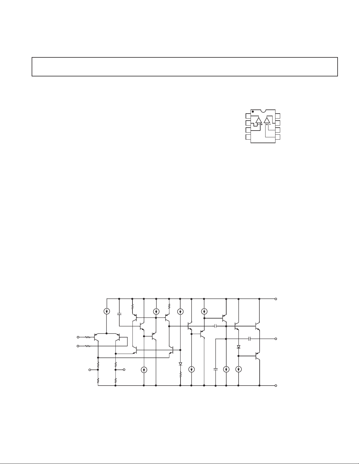
Figure 1. Simplified Schematic (one of two amplifiers is shown)
REV. B
Information furnished by Analog Devices is believed to be accurate and
reliable. However, no responsibility is assumed by Analog Devices for its
use, nor for any infringements of patents or other rights of third parties that
may result from its use. No license is granted by implication or otherwise
under any patent or patent rights of Analog Devices. Trademarks and
registered trademarks are the property of their respective owners.
V+
OUTPUT
V
One Technology Way, P.O. Box 9106, Norwood, MA 02062-9106, U.S.A.
Tel: 781/329-4700 www.analog.com
Fax: 781/326-8703 © 2003 Analog Devices, Inc. All rights reserved.

OP290–SPECIFICATIONS
ELECTRICAL CHARACTERISTICS
(@ VS = ⴞ1.5 V to ⴞ15 V, TA = 25ⴗC, unless otherwise noted.)
OP290G
Parameter Symbol Conditions Min Typ Max Unit
INPUT OFFSET VOLTAGE V
INPUT OFFSET CURRENT I
INPUT BIAS CURRENT I
LARGE-SIGNAL A
OS
OS
B
VO
VOLTAGE GAIN R
VCM = 0 V 0.1 5 nA
VCM = 0 V 4.0 25 nA
VS = ±15 V, VO = ±10 V
= 100 kΩ 400 600 V/mV
L
= 10 kΩ 200 400 V/mV
R
L
= 2 kΩ 100 200 V/mV
R
L
125 500 µV
V+ = 5 V, V– = 0 V,
1 V < V
R
R
INPUT VOLTAGE RANGE1IVR V+ = 5 V, V– = 0 V 0/4 V
V
OUTPUT VOLTAGE SWING V
O
VS = ±5 V
R
R
V
OH, VOL
V+ = 5 V, V– = 0 V 4.0 4.2 V
R
< 4 V
O
= 100 kΩ 100 250 V/mV
L
= 10 kΩ 70 140 V/mV
L
1
= ±5 V
S
= 10 kΩ±13.5 ±14.2 V
L
= 2 kΩ±10.5 ±11.5 V
L
= 10kΩ 10 50 µV
L
–15/13.5 V
COMMON-MODE CMR V+ = 5 V, V– = 0 V 80 100 dB
REJECTION 0 V < V
= ±15 V, 90 120 dB
V
S
–15 V < V
CM
CM
< 4 V
< +13.5 V
POWER SUPPLY PSRR 3.2 10 µV/V
REJECTION RATIO
SUPPLY CURRENT I
SY
(All Amplifiers) V
VS = ±1.5 V 19 30 µA
= ±15 V 25 40 µA
S
CAPACITIVE LOAD AV = +1 650 pF
STABILITY No Oscillations
INPUT NOISE VOLTAGE
INPUT RESISTANCE R
1
e
np-p
IN
fO = 0.1 Hz to 10 Hz 3 µV p-p
= ±15 V
V
S
VS = ±15 V 30 MΩ
DIFFERENTIAL-MODE
INPUT RESISTANCE R
INCM
VS = ±15 V 20 GΩ
COMMON-MODE
SLEW RATE SR AV = +1 5 12 V/ms
= ±15 V
V
S
GAIN BANDWIDTH GBWP Vs = +15 V 20 kHz
PRODUCT V
CHANNEL CS fO = 10 Hz 120 150 dB
SEPARATION
NOTES
1
Guaranteed by CMR test.
2
Guaranteed but not 100% tested.
Specifications subject to change without notice.
2
= ±15 V
S
VO = 20 V p-p
VS = ±15 V
2
–2–
REV. B

OP290
ELECTRICAL CHARACTERISTICS
(@ VS = ⴞ1.5 V to ⴞ15 V, –40ⴗC ≤ TA ≤ +85ⴗC for OP290G, unless otherwise noted.)
OP290G
Parameter Symbol Conditions Min Typ Max Unit
INPUT OFFSET VOLTAGE V
OS
AVERAGE INPUT OFFSET TCV
OS
VS = ±15 V 1.2 µV/°C
200 750 µV
VOLTAGE DRIFT
INPUT OFFSET CURRENT I
INPUT BIAS CURRENT I
LARGE-SIGNAL A
OS
B
VO
VOLTAGE GAIN R
VCM = 0 V 0.1 7 nA
VCM = 0 V 4.2 25 nA
VS = ±5 V, VO = ±0 V
= 100 kΩ 300 600 V/mV
L
RL = 10 kΩ 150 250 V/mV
R
= 2 kΩ 75 125 V/mV
L
V+ = 5 V, V– = 0 V,
< 4 V
O
= 100 kΩ 80 160 V/mV
L
= 10 kΩ 40 90 V/mV
L
= +15 V
S
= 10 kΩ±13 ±14 V
L
= 2 kΩ±10 ±11 V
L
= 2 kΩ 3.9 4.1 V
L
= 10 kΩ 10 100 µV
L
*
–15/+13.5 V
INPUT VOLTAGE RANGE
*
OUTPUT VOLTAGE SWING V
1 V < V
R
R
IVR V+ = 5 V, V– = 0 V 0/3.5 V
V
O
VS = ±15 V
R
R
V
OH
V+ = 5 V, V– = 0 V
R
V
OL
V+ = 5 V, V– = 0 V
R
COMMON-MODE CMR V+ = 5 V, V– = 0 V, 80 100 dB
REJECTION 0 V < V
= ±15 V
V
S
–15 V < V
< 3.5 V
CM
< 13.5 V 90 110 dB
CM
POWER SUPPLY PSRR 5.6 15 µV/V
REJECTION RATIO
SUPPLY CURRENT I
SY
VS = ±1.5 V 24 50 µA
(All Amplifiers) VS = ±15 V 31 60 µA
*
Guaranteed by CMR test.
Specifications subject to change without notice.
REV. B
–3–

OP290
ABSOLUTE MAXIMUM RATINGS
1
ORDERING GUIDE
Supply Voltage . . . . . . . . . . . . . . . . . . . . . . . . . . . . . . . . ±18 V
Differential Input Voltage . . . . [(V–) – 20 V] to [(V+) + 20 V]
Common-Mode Input Voltage . [(V–) – 20 V] to [(V+) + 20 V]
Output Short-Circuit Duration . . . . . . . . . . . . . . . . Indefinite
Storage Temperature Range
Model Range (mV)
OP290GP XIND 500 PDIP
Temperature V
P Package . . . . . . . . . . . . . . . . . . . . . . . . –65°C to +150°C
Operating Temperature Range
OP290G . . . . . . . . . . . . . . . . . . . . . . . . . . . –40°C to +85°C
Junction Temperature (T
) . . . . . . . . . . . . . –65°C to +150°C
J
Lead Temperature Range (Soldering, 60 sec) . . . . . . . . 300°C
Package Type
2
JA
JC
Unit
8-Lead Plastic DIP (P) 96 37 °C/W
NOTES
1
Absolute Maximum Ratings applies to packaged part.
2
JA is specified for worst-case mounting conditions, i.e., JA is specified for
device in socket for PDIP package.
CAUTION
ESD (electrostatic discharge) sensitive device. Electrostatic charges as high as 4000 V readily
accumulate on the human body and test equipment and can discharge without detection. Although
the OP290 features proprietary ESD protection circuitry, permanent damage may occur on devices
subjected to high energy electrostatic discharges. Therefore, proper ESD precautions are
recommended to avoid performance degradation or loss of functionality.
TA = 25ⴗC
Max
OS
WARNING!
Package
Description
ESD SENSITIVE DEVICE
–4–
REV. B

Typical Performance Characteristics–OP290
100
VS = 15V
80
60
40
20
INPUT OFFSET VOLTAGE – V
0
–75
TEMPERATURE – C
TPC 1. Input Offset Voltage vs.
Temperature
44
NO LOAD
40
36
32
28
24
20
16
SUPPLY CURRENT – A
12
8
4
–75
VS = 15V
VS = 1.5V
TEMPERATURE – C
TPC 4. Supply Current vs.
Temperature
VS = 15V
0.14
0.12
0.10
0.08
INPUT OFFSET CURRENT – nA
0.06
1251007550–50 –25 0 25
–75
TEMPERATURE – C
1251007550–50 –25 0 25
TPC 2. Input Offset Current vs.
Temperature
600
R
= 10k⍀
L
500
400
300
200
OPEN-LOOP GAIN – V/mV
100
0
1251007550–50 –25 0 25
0
TEMPERATURE – C
TA = 25 C
TA = 85 C
TA = 125 C
30252015510
TPC 5. Open-Loop Gain vs.
Single-Supply Voltage
4.5
VS = 15V
4.4
4.3
4.2
4.1
4.0
3.9
3.8
INPUT BIAS CURRENT – nA
3.7
3.6
3.5
–75
TEMPERATURE – C
1251007550–50 –25 0 25
TPC 3. Input Bias Current vs.
Temperature
140
120
100
80
60
40
OPEN-LOOP GAIN – dB
20
GAIN
0
0
FREQUENCY – Hz
PHASE
TA = 25 C
= 15V
V
S
= 100k⍀
R
L
140
120
100
80
60
40
20
0
30252015510
TPC 6. Open-Loop Gain and Phase
Shift vs. Frequency
PHASE SHIFT – Degrees
60
40
20
0
CLOSED-LOOP GAIN – dB
–20
10 100 100k
FREQUENCY – Hz
TA = 25 C
V
1k 10k
TPC 7. Closed-Loop Gain vs.
Frequency
REV. B
= 15V
S
6
TA = 25 C
V+ = 5V, V– = 0V
5
4
3
2
1
OUTPUT VOLTAGE SWING – V
0
100 1k 10k
LOAD RESISTANCE – ⍀
TPC 8. Ouput Voltage Swing vs.
Load Resistance
–5–
100k
16
14
12
10
8
6
4
OUTPUT VOLTAGE SWING – V
2
0
100 1k 10k
LOAD RESISTANCE – ⍀
= 25 C
T
A
V
= 15V
S
TPC 9. Output Voltage Swing
vs. Load Resistance
100k

OP290
140
T
= 25 C
A
120
100
80
60
POWER SUPPLY REJECTION – dB
40
110100
NEGATIVE SUPPLY
POSITIVE SUPPLY
FREQUENCY – Hz
TPC 10. Power Supply Rejection
vs. Frequency
10
TA = 25 C
= 15V
V
S
1
CURRENT NOISE DESTINY– nV/ Hz
0.1
0.1 1 1k
10 100
FREQUENCY – Hz
140
120
100
80
60
COMMON-MODE REJECTION – dB
40
1k
110100
FREQUENCY – Hz
TA = 25 C
= 15V
V
S
1k
TPC 11. Common-Mode Rejection
vs. Frequency
100
90
TA = 25 C
VS = 15V
AV = +1
RL = 10k⍀
CL = 500pF
10
0%
20mV
100s
1,000
TA = 25 C
= 15V
V
S
100
NOISE VOLTAGE DESTINY– nV/ Hz
10
0.1 1 1k
10 100
FREQUENCY – Hz
TPC 12. Noise Voltage Density
vs. Frequency
TA = 25 C
VS = 15V
AV = +1
100
RL = 10k⍀
90
CL = 500pF
10
0%
5V
1ms
TPC 13. Current Noise Density
vs. Frequency
TPC 14. Small-Signal Transient
Response
TPC 15. Large-Signal Transient
Response
–6–
REV. B

OP290
LITHIUM SULPHUR DIOXIDE
CELL VOLTAGE – V
100
80
0
0
60
40
20
350030002500500 1000 20001500
HOURS
+18V
100k⍀
200⍀
100k⍀
2
3
6
5
8
1/2
OP290
1/2
OP290
4
–18V
1
7
Figure 2. Burn-In Circuit
APPLICATIONS INFORMATION BATTERY-POWERED APPLICATIONS
The OP290 can be operated on a minimum supply voltage of
1.6 V, or with dual supplies of 0.8 V, and draws only 19 pA of
supply current. In many battery-powered circuits, the OP290
can be continuously operated for thousands of hours before
requiring battery replacement, reducing equipment downtime
and operating cost.
High-performance portable equipment and instruments frequently use lithium cells because of their long shelf-life, light
weight, and high energy density relative to older primary cells.
Most lithium cells have a nominal output voltage of 3 V and are
noted for a flat discharge characteristic. The low supply voltage
requirement of the OP290, combined with the flat discharge
characteristic of the lithium cell, indicates that the OP290 can
be operated over the entire useful life of the cell. Figure 1 shows
the typical discharge characteristic of a 1 Ah lithium cell powering an OP290 with each amplifier, in turn, driving full output
swing into a 100 kΩ load.
+15V
+15V
1/2
OP290
1k⍀
V
IN
A
–15V
1/2
OP290
B
9k⍀
OP37A
100⍀
CHANNEL SEPARATION = 20 LOG
10k⍀
–15V
V1 20Vp-p @ 10Hz
V2
V1
V2/1000
Figure 3. Channel Separation Test Circuit
APPLICATIONS TEMPERATURE TO 4–20 mA TRANSMITTER
A simple temperature to 4–20 mA transmitter is shown in Figure 5.
After calibration, the transmitter is accurate to +0.5°C over the
–50°C to +150°C temperature range. The transmitter operates
from 8 V to 40 V with supply rejection better than 3 ppm/V.
One half of the OP290 is used to buffer the V
pins while
TEMP
the other half regulates the output current to satisfy the current
summation at its noninverting input.
VRR
I
OUT
TEMP
=
+
67
()
RR
210
267
RRR
V
–
SET
RR
210
INPUT VOLTAGE PROTECTION
The OP290 uses a PNP input stage with protection resistors in
series with the inverting and noninverting inputs. The high
breakdown of the PNP transistors coupled with the protection
resistors provide a large amount of input protection, allowing
the inputs to be taken 20 V beyond either supply without damaging the amplifier.
SINGLE-SUPPLY OUTPUT VOLTAGE RANGE
In single-supply operation the OP290’s input and output ranges
include ground. This allows true “zero-in, zero-out” operation.
The output stage provides an active pull-down to around 0.8 V
above ground. Below this level, a load resistance of up to 1 MΩ
to ground is required to pull the output down to zero.
In the region from ground to 0.8 V, the OP290 has voltage gain
equal to the data sheet specification. Output current source capability is maintained over the entire voltage range including ground.
REV. B
Figure 4. Lithium Sulphur Dioxide Cell Discharge
Characteristic with OP290 and 100 k⍀ Loads
The change in output current with temperature is the derivative
of the transfer function:
V
∆
TEMP
RR
67
+
I
∆
OUT
=
T
∆
()
T
∆
RR
210
–7–

OP290
From the formulas, it can be seen that if the span trim is adjusted
before the zero trim, the two trims are not interactive, which
greatly simplifies the calibration procedure.
Calibration of the transmitter is simple. First, the slope of the
output current versus temperature is calibrated by adjusting the
span trim, R7. A couple of iterations may be required to be sure
the slope is correct.
Once the span trim has been completed, the zero trim can be made.
Remember that adjusting the offset trim will not affect the gain.
The offset trim can be set at any known temperature by adjusting
R
until the output current equals:
5
I
OUT
=
T
∆
∆
OPERATING
I
FS
TTmA
()
AMBIENT MIN
–4
+
Table I shows the values of R6 required for various temperature ranges.
Table I.
Temperature Range R6 (k⍀)
0°C to +70°C10
–40°C to +85°C 6.2
–55°C to +150°C3
VARIABLE SLEW RATE FILTER
The circuit shown in Figure 6 can be used to remove pulse noise
from an input signal without limiting the response rate to a genuine signal. The nonlinear filter has use in applications where
the input signal of interest is known to have physical limitations.
An example of this is a transducer output where a change of
temperature or pressure cannot exceed a certain rate due to
physical limitations of the environment. The filter consists of a
comparator which drives an integrator. The comparator compares the input voltage to the output voltage and forces the
integrator output to equal the input voltage. A1 acts as a comparator with its output high or low. Diodes D1 and D2 clamp
the voltage across R3 forcing a constant current to flow in or
out of C2. R3, C2, and A2 form an integrator with A2’s output
slewing at a maximum rate of:
Maximum slew rate
V
=≈
RCVRC
320632
.
D
For an input voltage slewing at a rate under this maximum slew
rate, the output simply follows the input with A1 operating in its
linear region.
REF-43BZ
V
V
OUT
TEMP
GND
1N4002
SPAN TRIM
V
SET
R6
3k⍀
6
1/2
OP290GP
5
R7
5k⍀
7
R8
1k⍀
R9
100k⍀
1%, 1/2W
R10
100⍀
2
V
IN
6
R1
3
10k⍀
4
2
1/2
OP290GP
8
4
V
TEMP
1
R3
100k⍀
1k⍀
R4
20k⍀
R2
R5
5k⍀
ZERO
TRIM
2N1711
I
OUT
R
LOAD
V+
8V TO 40V
Figure 5. Temperature to 4-20 mA Transmitter
–8–
REV. B

OP290
+15V
R1
250k⍀
C1
0.1F
D1
DIODES ARE 1N4148
D2
2
1/2
OP290GP
3
R3
1M⍀
6
1/2
OP290GP
5
–15V
8
R4
25k⍀
4
1
C1
4700pF
7
R2
100k⍀
V
OUT
Figure 6. Variable Slew Rate Filter
LOW OVERHEAD VOLTAGE REFERENCE
Figure 7 shows a voltage reference that requires only 0.1 V of
overhead voltage. As shown, the reference provides a stable
4.5 V output with a 4.6 V to 36 V supply. Output voltage drift is
only 12 ppm/°C. Line regulation of the reference is under 5 µV/V
with load regulation better than 10 µV/mA with up to 50 mA of
output current.
The REF-43 provides a stable 2.5 V which is multiplied by the
OP290. The PNP output transistor enables the output voltage
to approach the supply voltage.
Resistors R1 and R2 determine the output voltage.
The 200 Ω variable resistor is used to trim the output voltage.
For the lowest temperature drift, parallel resistors can be used in
place of the variable resistor and taken out of the circuit as required
to adjust the output voltage.
V+
2
V
IN
REF-43FZ
GND
4
6
V
OUT
BOURNS 3006P-1-201
R1B
200⍀
20-TURN
R1A
2.37⍀
1%
2
1/2
OP290GP
3
8
1
4
R2
2k⍀
1%
C1
10F
2N2907A
V
OUT
C2
0.1F
Figure 7. Low Overhead Voltage Reference
VV
OUT
=+
25 1
.
R
2
R
1
REV. B
–9–

OP290
OUTLINE DIMENSIONS
8-Lead Plastic Dual In-Line Package [PDIP]
[P-Suffix]
(N-8)
Dimensions shown in inches and (millimeters)
0.375 (9.53)
0.365 (9.27)
0.355 (9.02)
8
1
0.100 (2.54)
0.180
(4.57)
MAX
0.150 (3.81)
0.130 (3.30)
0.110 (2.79)
0.022 (0.56)
0.018 (0.46)
0.014 (0.36)
CONTROLLING DIMENSIONS ARE IN INCHES; MILLIMETER DIMENSIONS
(IN PARENTHESES) ARE ROUNDED-OFF INCH EQUIVALENTS FOR
REFERENCE ONLY AND ARE NOT APPROPRIATE FOR USE IN DESIGN
COMPLIANT TO JEDEC STANDARDS MO-095AA
BSC
5
4
0.295 (7.49)
0.285 (7.24)
0.275 (6.98)
0.015
(0.38)
MIN
SEATING
PLANE
0.060 (1.52)
0.050 (1.27)
0.045 (1.14)
0.325 (8.26)
0.310 (7.87)
0.300 (7.62)
0.150 (3.81)
0.135 (3.43)
0.120 (3.05)
0.015 (0.38)
0.010 (0.25)
0.008 (0.20)
–10–
REV. B

OP290
Revision History
Location Page
12/03—Data Sheet changed from REV. A to REV. B.
Deleted OP290E and OP290F . . . . . . . . . . . . . . . . . . . . . . . . . . . . . . . . . . . . . . . . . . . . . . . . . . . . . . . . . . . . . . . . . . . . . . .Universal
Replaced PIN CONNECTIONS with PDIP . . . . . . . . . . . . . . . . . . . . . . . . . . . . . . . . . . . . . . . . . . . . . . . . . . . . . . . . . . . . . . . . . . . 1
Deleted ELECTRICAL CHARACTERISTICS . . . . . . . . . . . . . . . . . . . . . . . . . . . . . . . . . . . . . . . . . . . . . . . . . . . . . . . . . . . . . . . . 3
Changes to ABSOLUTE MAXIMUM RATINGS . . . . . . . . . . . . . . . . . . . . . . . . . . . . . . . . . . . . . . . . . . . . . . . . . . . . . . . . . . . . . . 4
Changes to ORDERING GUIDE . . . . . . . . . . . . . . . . . . . . . . . . . . . . . . . . . . . . . . . . . . . . . . . . . . . . . . . . . . . . . . . . . . . . . . . . . . . 4
Changes to TPC 6 . . . . . . . . . . . . . . . . . . . . . . . . . . . . . . . . . . . . . . . . . . . . . . . . . . . . . . . . . . . . . . . . . . . . . . . . . . . . . . . . . . . . . . . 5
Change to SINGLE SUPPLY OUTPUT VOLTAGE RANGE . . . . . . . . . . . . . . . . . . . . . . . . . . . . . . . . . . . . . . . . . . . . . . . . . . . . 7
Changes to Figure 5 . . . . . . . . . . . . . . . . . . . . . . . . . . . . . . . . . . . . . . . . . . . . . . . . . . . . . . . . . . . . . . . . . . . . . . . . . . . . . . . . . . . . . . 8
Changes to Figure 6 . . . . . . . . . . . . . . . . . . . . . . . . . . . . . . . . . . . . . . . . . . . . . . . . . . . . . . . . . . . . . . . . . . . . . . . . . . . . . . . . . . . . . . 9
Change to LOW OVERHEAD VOLTAGE REFERENCE . . . . . . . . . . . . . . . . . . . . . . . . . . . . . . . . . . . . . . . . . . . . . . . . . . . . . . . . 9
Updated OUTLINE DIMENSIONS . . . . . . . . . . . . . . . . . . . . . . . . . . . . . . . . . . . . . . . . . . . . . . . . . . . . . . . . . . . . . . . . . . . . . . . 10
1/02—Data Sheet changed from REV. 0 to REV. A.
Edits to ORDERING INFORMATION . . . . . . . . . . . . . . . . . . . . . . . . . . . . . . . . . . . . . . . . . . . . . . . . . . . . . . . . . . . . . . . . . . . . . . 1
Edits to PIN CONNECTIONS . . . . . . . . . . . . . . . . . . . . . . . . . . . . . . . . . . . . . . . . . . . . . . . . . . . . . . . . . . . . . . . . . . . . . . . . . . . . . 1
Edits to ABSOLUTE MAXIMUM RATINGS . . . . . . . . . . . . . . . . . . . . . . . . . . . . . . . . . . . . . . . . . . . . . . . . . . . . . . . . . . . . . . . . . 2
Edits to PACKAGE TYPE . . . . . . . . . . . . . . . . . . . . . . . . . . . . . . . . . . . . . . . . . . . . . . . . . . . . . . . . . . . . . . . . . . . . . . . . . . . . . . . . 2
Edits to WAFER TEST LIMITS . . . . . . . . . . . . . . . . . . . . . . . . . . . . . . . . . . . . . . . . . . . . . . . . . . . . . . . . . . . . . . . . . . . . . . . . . . . 5
Edits to DICE CHARACTERISTICS . . . . . . . . . . . . . . . . . . . . . . . . . . . . . . . . . . . . . . . . . . . . . . . . . . . . . . . . . . . . . . . . . . . . . . . 5
REV. B
–11–

C00327–0–12/03(B)
–12–
 Loading...