


REV. A
Information furnished by Analog Devices is believed to be accurate and
reliable. However, no responsibility is assumed by Analog Devices for its
use, nor for any infringements of patents or other rights of third parties that
may result from its use. No license is granted by implication or otherwise
under any patent or patent rights of Analog Devices.
a
OP285
*
One Technology Way, P.O. Box 9106, Norwood, MA 02062-9106, U.S.A.
Tel: 781/329-4700 www.analog.com
Fax: 781/326-8703 © Analog Devices, Inc., 2001
Dual 9 MHz Precision
Operational Amplifier
PIN CONNECTIONS
8-Lead Narrow-Body SO (S-Suffix)
TOP VIEW
(Not to Scale)
OP285
–IN A
+IN A
V–
OUT A
V+
–IN B
+IN B
OUT B
8
7
6
5
1
2
3
4
8-Lead Epoxy DIP (P-Suffix)
8
7
6
5
V+
–IN B
+IN B
OUT B
1
2
3
4
–IN A
+IN A
V–
OUT A
+–
+–
OP285
The combination of low noise, speed and accuracy can be used
to build high speed instrumentation systems. Circuits such as
instrumentation amplifiers, ramp generators, bi-quad filters and
dc-coupled audio systems are all practical with the OP285. For
applications that require long term stability, the OP285 has a
guaranteed maximum long term drift specification.
The OP285 is specified over the XIND—extended industrial—
(–40°C to +85°C) temperature range. OP285s are available in
8-pin plastic DIP and SOIC-8 surface mount packages.
FEATURES
Low Offset Voltage: 250 V
Low Noise: 6 nV/√ Hz
Low Distortion: 0.0006%
High Slew Rate: 22 V/s
Wide Bandwidth: 9 MHz
Low Supply Current: 5 mA
Low Offset Current: 2 nA
Unity-Gain Stable
SO-8 Package
APPLICATIONS
High Performance Audio
Active Filters
Fast Amplifiers
Integrators
GENERAL DESCRIPTION
The OP285 is a precision high-speed amplifier featuring the
Butler Amplifier front-end. This new front-end design combines the accuracy and low noise performance of bipolar
transistors with the speed of JFETs. This yields an amplifier
with high slew rates, low offset and good noise performance
at low supply currents. Bias currents are also low compared
to bipolar designs.
The OP285 offers the slew rate and low power of a JFET
amplifier combined with the precision, low noise and low
drift of a bipolar amplifier. Input offset voltage is laser-trimmed
and guaranteed less than 250 µV. This makes the OP285 useful
in dc-coupled or summing applications without the need for
special selections or the added noise of additional offset
adjustment circuitry. Slew rates of 22 V/µs and a bandwidth
of 9 MHz make the OP285 one of the most accurate medium
speed amplifiers available.
*Patents pending

REV. A
–2–
OP285–SPECIFICATIONS
(@ Vs = 15.0 V, TA = 25C, unless otherwise noted.)
Parameter Symbol Conditions Min Typ Max Unit
INPUT CHARACTERISTICS
Offset Voltage V
OS
35 250 µV
V
OS
–40°C ≤ TA ≤ +85°C 600 µV
Input Bias Current I
B
VCM = 0 V 100 350 nA
I
B
VCM = 0 V, –40°C ≤ TA ≤ +85°C 400 nA
Input Offset Current I
OS
VCM = 0 V 2 ±50 nA
I
OS
VCM = 0 V, –40°C ≤ TA ≤ +85°C2±100 nA
Input Voltage Range V
CM
–10.5 10.5 V
Common-Mode Rejection CMRR V
CM
= ±10.5 V,
–40°C ≤ T
A
≤ +85°C 80 106 dB
Large-Signal Voltage Gain A
VO
RL = 2 kΩ 250 V/mV
A
VO
RL = 2 kΩ, –40°C ≤ TA ≤ +85°C 175 V/mV
A
VO
RL = 600 Ω 200 V/mV
Common-Mode Input Capacitance 7.5 pF
Differential Input Capacitance 3.7 pF
Long-Term Offset Voltage ∆V
OS
Note 1 300 µV
Offset Voltage Drift ∆V
OS
/∆T1µV/°C
OUTPUT CHARACTERISTICS
Output Voltage Swing V
O
RL = 2 kΩ –13.5 +13.9 +13.5 V
V
O
RL = 2 kΩ, –40°C ≤ TA ≤ +85°C –13 +13.9 +13 V
RL = 600 Ω, V
S
= ±18 V –16/+14 V
POWER SUPPLY
Power Supply Rejection Ratio PSRR V
S
= ±4.5 V to ±18 V 85 111 dB
PSRR V
S
= ±4.5 V to ±18 V,
–40°C ≤ T
A
≤ +85°C80 dB
Supply Current I
SY
VS = ±4.5 V to ±18 V, VO = 0 V,
R
L
= x, –40°C ≤ TA ≤ +85°C45mA
I
SY
VS = ±22 V, VO, = 0 V, RL = x
–40°C ≤ T
A
≤ +85°C 5.5 mA
Supply Voltage Range VS ±4.5 ± 22 V
DYNAMIC PERFORMANCE
Slew Rate SR R
L
= 2 kΩ 15 22 V/µs
Gain Bandwidth Product GBP 9 MHz
Phase Margin o 62 Degrees
Settling Time t
s
To 0.1%, 10 V Step 625 ns
t
s
To 0.01%, 10 V Step 750 ns
Distortion A
V
= 1, V
OUT
= 8.5 V p-p,
f = 1 kHz, R
L
= 2 kΩ –104 dB
Voltage Noise Density e
n
f = 30 Hz 7 nV/√Hz
e
n
f = 1 kHz 6 nV/√Hz
Current Noise Density i
n
f = 1 kHz 0.9 pA/√Hz
Headroom THD + Noise ≤ 0.01%,
RL = 2 kΩ, VS = ±18 V >12.9 dBu
NOTE
1
Long-term offset voltage is guaranteed by a 1,000 hour life test performed on three independent wafer lots at 125 °C, with an LTPD of 1.3.
Specifications subject to change without notice.

REV. A
–3–
OP285
CAUTION
ESD (electrostatic discharge) sensitive device. Electrostatic charges as high as 4000 V readily
accumulate on the human body and test equipment and can discharge without detection. Although
the OP285 features proprietary ESD protection circuitry, permanent damage may occur on devices
subjected to high-energy electrostatic discharges. Therefore, proper ESD precautions are
recommended to avoid performance degradation or loss of functionality.
WARNING!
ESD SENSITIVE DEVICE
ABSOLUTE MAXIMUM RATINGS
1
Supply Voltage . . . . . . . . . . . . . . . . . . . . . . . . . . . . . . . . ±22 V
Input Voltage
2
. . . . . . . . . . . . . . . . . . . . . . . . . . . . . . . . ±18 V
Differential Input Voltage
2
. . . . . . . . . . . . . . . . . . . . . . ±7.5 V
Output Short-Circuit Duration to Gnd
3
. . . . . . . . . Indefinite
Storage Temperature Range
P, S Package . . . . . . . . . . . . . . . . . . . . . . . –65°C to +150°C
Operating Temperature Range
OP285G . . . . . . . . . . . . . . . . . . . . . . . . . . . –40°C to +85°C
Junction Temperature Range
P, S Package . . . . . . . . . . . . . . . . . . . . . . . –65°C to +150°C
Lead Temperature Range (Soldering 60 Sec) . . . . . . . . 300°C
Package Type
JA
4
JC
Unit
8-Pin Plastic DIP (P) 103 43 °C/W
8-Pin SOIC (S) 158 43 °C/W
NOTES
1
Absolute Maximum Ratings apply to packaged parts, unless otherwise noted.
2
For supply voltages less than ± 7.5 V, the absolute maximum input voltage is
equal to the supply voltage.
3
Shorts to either supply may destroy the device. See data sheet for full details.
4
JA is specified for the worst case conditions, i.e., JA is specified for device in
socket for cerdip, P-DIP, and LCC packages; JA is specified for device soldered
in circuit board for SOIC package.
ORDERING GUIDE
Temperature Package Package
Model Range Description Option
OP285GP* –40°C to +85°C 8-Pin Plastic DIP N-8
OP285GS –40°C to +85°C 8-Pin SOIC S0-8
OP285GSR –40°C to +85°C S0-8 Reel, 2500 pcs.
*Not for new designs. Obsolete April 2002.
REV. A
OP285
–4–
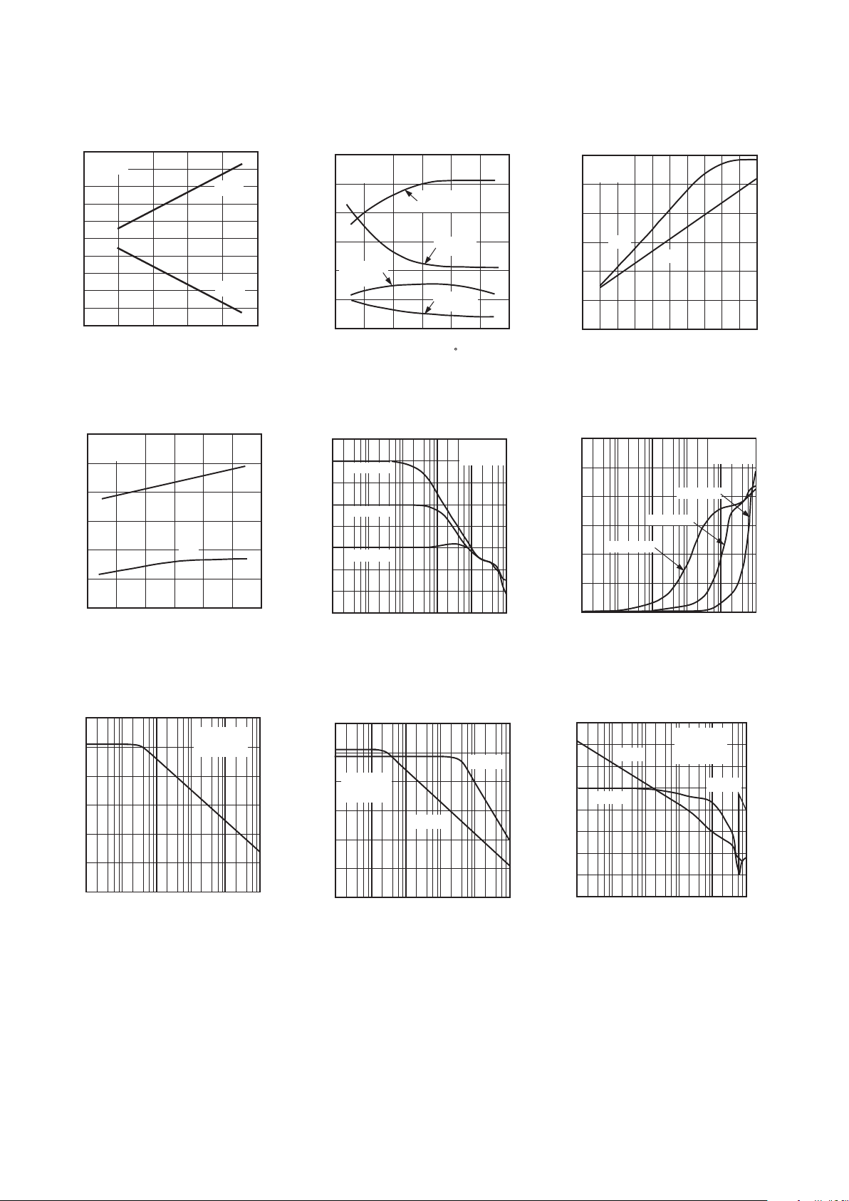
25
–25
–10
–20
–15
5
–5
0
10
15
20
OUTPUT VOLTAGE SWING – V
SUPPLY VOLTAGE – V
+VOM
–VOM
0 5 10 15 20 25
T
A
= 25C
R
L
= 2k
TPC 1. Output Voltage Swing vs.
Supply Voltage
50
20
35
25
30
45
40
–SR
+SR
100–25–50 755025
0
TEMPERATURE – C
VS = 15V
R
L
= 2k
SLEW RATE – V/s
VS = 15V
R
L
= 2k
TPC 4. Slew Rate vs. Temperature
120
100
60
0
1k 10k 100k 1M 10M
40
20
80
100
COMMON MODE REJECTION – dB
FREQUENCY – Hz
V
S
= 15V
T
A
= 25C
TPC 7. Common-Mode Rejection
vs. Frequency
1500
0
100
750
250
–25
500
–50
1250
1000
755025
0
OPEN-LOOP GAIN – V/MV
TEMPERATURE – C
VS = 15V
V
O
= 10V
+GAIN
R
L
= 2k
–GAIN
R
L
= 2k
–GAIN
R
L
= 600
+GAIN
R
L
= 600
TPC 2. Open-Loop Gain
vs. Temperature
50
1k
10
–30
10k 100k 1M 10M 100M
20
30
40
–20
–10
0
CLOSED-LOOP GAIN – dB
FREQUENCY – Hz
VS = 15V
T
A
= +25C
A
VCL
= +100
A
VCL
= +10
A
VCL
= +1
TPC 5. Closed-Loop Gain
vs. Frequency
120
10
60
0
100 1k 10k 100k 1M
40
20
80
100
+PSRR
–PSRR
FREQUENCY – Hz
POWER SUPPLY REJECTION – dB
VS = 15V
T
A
= 25C
TPC 8. Power Supply Rejection
vs. Frequency
30
0
1.0
15
5
10
0
25
20
0.80.60.40.2
SLEW RATE – V/s
DIFFERENTIAL INPUT VOLTAGE – V
–SR
+SR
VS = 15V
R
L
= 2k
TPC 3. Slew Rate vs. Differential
Input Voltage
60
100
30
0
1k 10k 100k 1M 10M
20
10
40
50
FREQUENCY – Hz
IMPEDANCE –
A
VCL
= +1
A
VCL
= +100
A
VCL
= +10
VS = 15V
T
A
= 25C
TPC 6. Closed-Loop Output Imped
ance vs. Frequency
100
1k
20
–60
10k 100k 1M 10M 100M
40
60
80
–40
–20
0
0
45
90
135
180
225
270
OPEN-LOOP G
MIN
– dB
PHASE – Degrees
PHASE
GAIN
FREQUENCY – Hz
V
S
= 15V
R
L
= 2k
T
A
= 25C
0
N
= 58
TPC 9. Open-Loop Gain, Phase
vs. Frequency
REV. A
–5–
Typical Performance Characteristics–OP285
11
7
–50 100
10
8
–25 755025
0
9
40
50
55
60
65
TEMPERATURE – C
GAIN BANDWIDTH PRODUCT – MHz
PHASE MARGIN – Degrees
GBW
M
ø
TPC 10. Gain Bandwidth Product,
Phase Margin vs. Temperature
30
15
0
1k
10k 10M1M100k
10
5
20
25
TA = 25C
V
S
= 15V
A
VCL
= +1
R
L
= 2k
FREQUENCY – Hz
MAXIMUM OUTPUT SWING – V
TPC 13. Maximum Output Swing
vs. Frequency
300
0
100
150
50
–25
100
–50
250
200
755025
0
VS = 15V
TEMPERATURE – C
INPUT BIAS CURRENT – nA
TPC 16. Input Bias Current vs.
Temperature
100
0
500
30
10
100
20
0
60
40
50
70
80
90
400200
300
LOAD CAPACITANCE – pF
OVERSHOOT – %
VS = 15V
R
L
= 2k
V
IN
= 100mV p-p
A = +1
NEGATIVE EDGE
VCL
A = +1
POSITIVE EDGE
VCL
TPC 11. Small-Signal Overshoot vs.|
Load Capacitance
5.0
3.0
25
4.5
3.5
5
4.0
1510
0
TA = +25C
TA = +85C
TA = –40C
SUPPLY CURRENT – mA
SUPPLY VOLTAGE – V
TPC 14. Supply Current vs.
Supply Voltage
FREQUENCY – Hz
10
100 100k1k
5
4
3
2
1
CURRENT NOISE DENSITY – pA/
Hz
VS = 15V
T
A
= 25C
TPC 17. Current Noise Density vs.
Frequency
16
8
0
100 1k 10k
2
4
6
10
12
14
LOAD RESISTANCE –
MAXIMUM OUTPUT SWING – Volts
TA = 25C
V
S
= 15V
+VOM
–VOM
TPC 12. Maximum Output Voltage
vs. Load Resistance
120
20
100
50
30
–25
40
–50
80
60
70
90
100
110
7525 50
0
TEMPERATURE – C
ABSOLUTE OUTPUT CURRENT – mA
VS = 15V
SOURCE
SINK
TPC 15. Short Circuit Current vs.
Temperature
250
0
10
150
50
1
100
0
200
98765432
UNITS
TC V
OS
– V/ C
–40C TA +85C
402 OP AMPS
TPC 18. tC VOS Distribution

REV. A
OP285
–6–
250
0
250
150
50
100
–250
200
15050
0
–150
UNITS
TA= 25C
402 OP AMPS
INPUT OFFSET – V
–50–100
–
2
00
200100
TPC 19. Input Offset (VOS)
Distribution
10
0%
100
90
200nS
5V
TPC 22. Negative Slew Rate
R
L
=2 kΩ, VS = ±15 V, AV = +1
0 Hz
2.5 KHz
BW: 15.0 MHzMKR: 1 000 Hz
CH A: 80.0 V FS 10.0 V/DIV
MKR: 6.23 V/
Hz
TPC 25. OP285 Voltage Noise Density
vs. Frequency V
S
= ±15 V, AV = 1000
10
–10
900
–4
–8
100
–6
0
2
–2
0
4
6
8
800500 600300 400 700200
STEP SIZE – V
SETTLING TIME – ns
+0.1%
+0.01%
–0.1% –0.01%
TPC 20. Settling Time vs. Step Size
10
0%
100
90
200nS
5V
TPC 23. Positive Slew Rate
RL = 2 k
Ω
, VS = ±15 V, AV = +1
50
20
500
35
25
100
30
0
45
40
400300200
CAPACITIVE LOAD – pF
SLEW RATE – V/S
TA = 25C
V
S
= 15V
–SR
+SR
TPC 21. Slew Rate vs.
Capacitive Load
10
0%
100
90
100nS
50mV
TPC 24. Small Signal Response
R
L
=2 kΩ, VS = ±15 V, AV = +1

REV. A
OP285
–7–
APPLICATIONS
Short-Circuit Protection
The OP285 has been designed with inherent short-circuit
protection to ground. An internal 30 Ω resistor, in series with
the output, limits the output current at room temperature to
I
SC
+ = 40 mA and ISC- = –90 mA, typically, with ±15 V supplies.
However, shorts to either supply may destroy the device when
excessive voltages or current are applied. If it is possible for a
user to short an output to a supply, for safe operation, the output current of the OP285 should be design-limited to ±30 mA,
as shown in Figure 1.
R
FB
FEEDBACK
R
X
332
A1
V
OUT
A1 = 1/2 OP285
–
+
Figure 1. Recommended Output Short-Circuit Protection
Input Over Current Protection
The maximum input differential voltage that can be applied
to the OP285 is determined by a pair of internal Zener diodes
connected across the inputs. They limit the maximum differential input voltage to ±7.5 V. This is to prevent emitter-base
junction breakdown from occurring in the input stage of the
OP285 when very large differential voltages are applied. However, in order to preserve the OP285’s low input noise
voltage, internal resistance in series with the inputs were not
used to limit the current in the clamp diodes. In small-signal
applications, this is not an issue; however, in industrial applications, where large differential voltages can be inadvertently
applied to the device, large transient currents can be made to
flow through these diodes. The diodes have been designed to
carry a current of ±8 mA; and, in applications where the
OP285’s differential voltage were to exceed ±7.5 V, the resistor values shown in Figure 2 safely limit the diode current to
±8 mA.
A1
909
A1 = 1/2
909
–
+
Figure 2. OP285 Input Over Current Protection
Output Voltage Phase Reversal
Since the OP285’s input stage combines bipolar transistors
for low noise and p-channel JFETs for high speed performance,
the output voltage of the OP285 may exhibit phase reversal if
either of its inputs exceed its negative common-mode input
voltage. This might occur in very severe industrial applications
where a sensor or system fault might apply very large voltages on
the inputs of the OP285. Even though the input voltage range of
the OP285 is ±10.5 V, an input voltage of approximately –13.5 V
will cause output voltage phase reversal. In inverting amplifier
configurations, the OP285’s internal 7.5 V input clamping
diodes will prevent phase reversal; however, they will not prevent
this effect from occurring in noninverting applications. For these
applications, the fix is a simple one and is illustrated in Figure 3.
A 3.92 kΩ resistor in series with the noninverting input of the
OP285 cures the problem.
RFB*
V
IN
RS
3.92k
V
OUT
RL
2k
*R
FB
IS OPTIONAL
+
–
Figure 3. Output Voltage Phase Reversal Fix
Overload or Overdrive Recovery
Overload or overdrive recovery time of an operational amplifier
is the time required for the output voltage to recover to a rated
output voltage from a saturated condition. This recovery time is
important in applications where the amplifier must recover quickly
after a large abnormal transient event. The circuit shown in Figure
4 was used to evaluate the OP285’s overload recovery time. The
OP285 takes approximately 1.2 µs to recover to V
OUT
= +10 V
and approximately 1.5 µs to recover to V
OUT
= –10 V.
V
IN
4V p-p
@100 Hz
V
OUT
RL
2.43k
A1 = 1/2 OP285
R2
10k
R1
1k
1
2
3
A1
R
S
909
Figure 4. Overload Recovery Time Test Circuit
Driving the Analog Input of an A/D Converter
Settling characteristics of operational amplifiers also include the
amplifier’s ability to recover, i.e., settle, from a transient output
current load condition. When driving the input of an A/D
converter, especially successive-approximation converters, the
amplifier must maintain a constant output voltage under
dynamically changing load current conditions. In these types of
converters, the comparison point is usually diode clamped, but
it may deviate several hundred millivolts resulting in high
frequency modulation of the A/D input current. Amplifiers that
exhibit high closed-loop output impedances and/or low unity-gain
crossover frequencies recover very slowly from output load
current transients. This slow recovery leads to linearity errors or
missing codes because of errors in the instantaneous input voltage.
Therefore, the amplifier chosen for this type of application should
exhibit low output impedance and high unity-gain bandwidth so
that its output has had a chance to settle to its nominal value
before the converter makes its comparison.
The circuit in Figure 5 illustrates a settling measurement circuit
for evaluating the recovery time of an amplifier from an output
load current transient. The amplifier is configured as a follower
with a very high speed current generator connected to its output.
In this test, a 1 mA transient current was used. As shown in
Figure 6, the OP285 exhibits an extremely fast recovery time of
139 ns to 0.01%. Because of its high gain-bandwidth product,
high open-loop gain, and low output impedance, the OP285 is
ideally suited to drive high speed A/D converters.

REV. A
OP285
–8–
16–20V
0.1F
V+
V–
5V
D1 D2
+15V
2N4416
D3
D4
OUTPUT
(TO SCOPE)
1F
IC2
2N2222A
–15V
1N4148
DUT
1/2 OP260AJ
16–20V
– +
+ –
SCHOTTKY DIODES D1–D4 ARE
HEWLETT-PACKARD HP5082-2835
IC1 IS 1/2 OP260AJ
IC2 IS PMI OP41EJ
15k
R
L
1k
0.1F
10k
10k
R
F
2k
R
G
222
750
1k
+15V
3
8
1
4
2
–15V
+ 7A13 PLUG-IN
– 7A13 PLUG-IN
2N3904
300pF
15V
1N4148
TTL
INPUT
15V
1.8k
0.1F
V
REF
(–1V)
2N2907
I
OUT
|V
REF
|
1k
*NOTE
DECOUPLE CLOSE
TOGETHER ON GROUND PLAN
WITH SHORT LEAD LENGTHS.
*
0.01F
0.47F
+
10F
0.1F
0.1F
220
1k
1k
1.5k
1/2
OP285
+
–
Figure 5. Transient Output Load Current Test Fixture
10
90
100
0%
A1 1,2 V T 138.9
NS
5V
TTL CTRL
(5V/ DIV)
10V
V
OUT
(2MV/ DIV)
2MV
50NS
Figure 6. OP285’s Output Load Current Recovery Time
Measuring Settling Time
The design of OP285 combines high slew rate and wide gainbandwidth product to produce a fast-settling (ts < l µs) amplifier
for 8- and 12-bit applications. The test circuit designed to measure
the settling time of the OP285 is shown in Figure 7. This test
method has advantages over false-sum node techniques in that
the actual output of the amplifier is measured, instead of an
error voltage at the sum node. Common-mode settling effects
are exercised in this circuit in addition to the slew rate and
bandwidth effects measured by the false-sum-node method. Of
course, a reasonably flat-top pulse is required as the stimulus.
The output waveform of the OP285 under test is clamped by
Schottky diodes and buffered by the JFET source follower.
The signal is amplified by a factor of ten by the OP260 and
then Schottky-clamped at the output to prevent overloading
the oscilloscope’s input amplifier. The OP41 is configured as
a fast integrator which provides overall dc offset nulling.
High Speed Operation
As with most high speed amplifiers, care should be taken with
supply decoupling, lead dress, and component placement. Recommended circuit configurations for inverting and noninverting
applications are shown in Figures 8 and Figure 9.
+15V
+
2
3
8
1
4
V
IN
V
OUT
–15V
10F
0.1F
R
L
15k
0.1F
10F
+
–
1/2
OP285
Figure 8. Unity Gain Follower
Figure 7. OP285’s Settling Time Test Fixture

REV. A
OP285
–9–
+15V
+
2
3
8
1
4
V
IN
V
OUT
–15V
10pF
+
10F
0.1F
4.99k
2k
0.1F
10F
2.49k
4.99k
+
–
1/2
OP285
Figure 9. Unity-Gain Inverter
In inverting and noninverting applications, the feedback resistance forms a pole with the source resistance and capacitance
(R
S
and CS) and the OP285’s input capacitance (CIN), as
shown in Figure 10. With R
S
and RF in the kilohm range, this
pole can create excess phase shift and even oscillation. A small
capacitor, C
FB
, in parallel with RFB eliminates this problem. By
setting R
S
(CS + CIN) = RFBCFB, the effect of the feedback pole
is completely removed.
C
FB
R
FB
C
IN
V
OUT
R
S
C
S
Figure 10. Compensating the Feedback Pole
High-Speed, Low-Noise Differential Line Driver
The circuit of Figure 11 is a unique line driver widely used in
industrial applications. With ±18 V supplies, the line driver can
deliver a differential signal of 30 V p-p into a 2.5 kΩ load. The
high slew rate and wide bandwidth of the OP285 combine to
yield a full power bandwidth of 130 kHz while the low noise
front end produces a referred-to-input noise voltage spectral
density of 10 nV/√Hz. The design is a transformerless, balanced
transmission system where output common-mode rejection of
noise is of paramount importance. Like the transformer-based
design, either output can be shorted to ground for unbalanced
line driver applications without changing the circuit gain of 1.
Other circuit gains can be set according to the equation in the
diagram. This allows the design to be easily set to noninverting,
inverting, or differential operation.
2
3
A2
1
3
2
A1
5
6
7
A3
V
IN
V
O1
V
O2
V
O2
– VO1 = V
IN
R2
2k
A1 = 1/2OP285
A2, A3 = 1/2 OP285
GAIN = SET R2, R4, R5 = R1 AND R, R7, R8 = R2
1
R1
2k
R3
2k
R9
50
R11
1k
P1
10k
R12
1k
R4
2k
R5
2k
R6
2k
R10
50
R8
2k
R7
2k
Figure 11. High-Speed, Low-Noise Differential Line Driver
Low Phase Error Amplifier
The simple amplifier configuration of Figure 12 uses the OP285
and resistors to reduce phase error substantially over a wide
frequency range when compared to conventional amplifier designs.
This technique relies on the matched frequency characteristics
of the two amplifiers in the OP285. Each amplifier in the circuit
has the same feedback network which produces a circuit gain of
10. Since the two amplifiers are set to the same gain and are
matched due to the monolithic construction of the OP285, they
will exhibit identical frequency response. Recall from feedback
theory that a pole of a feedback network becomes a zero in the
loop gain response. By using this technique, the dominant pole
of the amplifier in the feedback loop compensates for the dominant pole of the main amplifier,
1
2
3
A1
7
A2
5
6
R1
549
R2
4.99k
R3
499
V
IN
V
OUT
R5
549
R4
4.99
A1, A2 = 1/2 OP285
Figure 12. Cancellation of A2’s Dominant Pole by A1

REV. A
OP285
–10–
thereby reducing phase error dramatically. This is shown in
Figure 13 where the 10x composite amplifier’s phase response
exhibits less than 1.5° phase shift through 500 kHz. On the other
hand, the single gain stage amplifier exhibits 25° of phase shift
over the same frequency range. An additional benefit of the low
phase error configuration is constant group delay, by virtue of
constant phase shift at all frequencies below 500 kHz. Although
this technique is valid for minimum circuit gains of 10, actual
closed-loop magnitude response must be optimized for the
amplifier chosen.
–20
–45
10k 100k 10M1M
–25
–30
–35
–40
–15
–10
–5
0
START 10,000.000Hz STOP 10,000,000.000Hz
PHASE – Degrees
SINGLE STAGE
AMPLIFIER RESPONSE
LOW PHASE ERROR
AMPLIFIER RESPONSE
Figure 13. Phase Error Comparison
For a more detailed treatment on the design of low phase error
amplifiers, see Application Note AN-107.
Fast Current Pump
A fast, 30 mA current source, illustrated in Figure 14, takes
advantage of the OP285’s speed and high output current drive.
This is a variation of the Howland current source where a second amplifier, A2, is used to increase load current accuracy and
output voltage compliance. With supply voltages of ±15 V, the
output voltage compliance of the current pump is ±8 V. To
keep the output resistance in the MΩ range requires that 0.1%
or better resistors be used in the circuit. The gain of the current
pump can be easily changed according to the equations shown
in the diagram.
1
2
3
A1
5
6
7
V
IN1
V
IN2
A2
A1, A2 = 1/2 OP285
R2
R1
GAIN = , R4 = R2, R3 = R1
R1
2k
R2
2k
R5
50
R3
2k
R4
2k
I
OUT
=
V
IN2
– V
IN1
R5
V
IN
R5
=
I
OUT
= (MAX) = 30mA
Figure 14. A Fast Current Pump
A Low Noise, High Speed Instrumentation Amplifier
A high speed, low noise instrumentation amplifier, constructed
with a single OP285, is illustrated in Figure 15. The circuit exhibits
less than 1.2 µV p-p noise (RTI) in the 0.1 Hz to 10 Hz band
and an input noise voltage spectral density of 9 nV/√Hz (1 kHz)
at a gain of 1000. The gain of the amplifier is easily set by R
G
according to the formula:
V
V
k
R
OUT
IN G
=+
9982. Ω
The advantages of a two op amp instrumentation amplifier
based on a dual op amp is that the errors in the individual amplifiers tend to cancel one another. For example, the circuit’s
input offset voltage is determined by the input offset voltage
matching of the OP285, which is typically less than 250 µV.
1
2
3
A2
A1
5
6
7
V
IN
A1, A2 = 1/2 OP285
R
Q
9.98k
+2
GAIN =
R
G
()
OPEN
1.24k
102
10
2
10
100
1000
GAIN
R1
4.99k
P1
500
DC CMRR TRIM
AC CMRR TRIM
C1
5pF–40pF
+
–
R
G
R2
4.99
R3
4.99k
R4
4.99k
V
OUT
Figure 15. A High-Speed Instrumentation Amplifier
Common-mode rejection of the circuit is limited by the matching
of resistors R1 to R4. For good common-mode rejection, these
resistors ought to be matched to better than 1%. The circuit was
constructed with 1% resistors and included potentiometer P1
for trimming the CMRR and a capacitor C1 for trimming the
CMRR. With these two trims, the circuit’s common-mode
rejection was better than 95 dB at 60 Hz and better than 65 dB
at 10 kHz. For the best common-mode rejection performance,
use a matched (better than 0.1%) thin-film resistor network for
R1 through R4 and use the variable capacitor to optimize the
circuit’s CMR.
The instrumentation amplifier exhibits very wide small- and
large-signal bandwidths regardless of the gain setting, as shown
in the table. Because of its low noise, wide gain-bandwidth
product, and high slew rate, the OP285 is ideally suited for high
speed signal conditioning applications.
Circuit R
G
Circuit Bandwidth
Gain () V
OUT
= 100 mV p-p V
OUT
= 20 V p-p
2 Open 5 MHz 780 kHz
10 1.24 k 1 MHz 460 kHz
100 102 90 kHz 85 kHz
1000 10 10 kHz 10 kHz

REV. A
OP285
–11–
A 3-Pole, 40 kHz Low-Pass Filter
The closely matched and uniform ac characteristics of the OP285
make it ideal for use in GIC (Generalized Impedance Converter)
and FDNR (Frequency Dependent Negative Resistor) filter applications. The circuit in Figure 16 illustrates a linear-phase,
3-pole, 40 kHz low-pass filter using an OP285 as an inductance
simulator (gyrator). The circuit uses one OP285 (A2 and A3)
for the FDNR and one OP285 (Al and A4) as an input buffer
and bias current source for A3. Amplifier A4 is configured in a
gain of 2 to set the pass band magnitude response to 0 dB. The
benefits of this filter topology over classical approaches are
that the op amp used in the FDNR is not in the signal path and
that the filter’s performance is relatively insensitive to component variations. Also, the configuration is such that large signal
levels can be handled without overloading any of the filter’s
internal nodes. As shown in Figure 17, the OP285’s symmetric
slew rate and low distortion produce a clean, well-behaved
transient response.
10
90
100
0%
SCALE: VERTICAL – 2V/ DIV
HORIZONTAL – 10S/ DIV
V
OUT
10V p-p
10kHz
Figure 17. Low-Pass Filter Transient Response
V
IN
3
2
1
A1
A1, A4 = 1/2 OP285
A2, A3 = 1/2 OP285
1
A2
2
3
R1
95.3k
C1
2200pF
R2
787
C2
2200pF
R3
1.82k
C3
2200pF
R4
1.87k
R5
1.82k
A3
5
7
6
A4
5
7
6
R6
4.12k
R7
100k
R9
1k
V
OUT
R8
1k
C4
2200pF
Figure 16. A 3-Pole, 40 kHz Low-Pass Filter
Driving Capacitive Loads
The OP285 was designed to drive both resistive loads to 600 Ω
and capacitive loads of over 1000 pF and maintain stability. While
there is a degradation in bandwidth when driving capacitive loads,
the designer need not worry about device stability. The graph in
Figure 18 shows the 0 dB bandwidth of the OP285 with capacitive
loads from 10 pF to 1000 pF.
0
0
C
LOAD
– pF
BANDWIDTH – MHz
200 400 600 800 1000
1
2
3
4
5
6
7
8
9
10
Figure 18. Bandwidth vs. C
LOAD

REV. A
OP285
–12–
OP285 SPICE Model
* Node assignments
* noninverting input
* inverting input
* positive supply
* negative supply
* output
*
*
.SUBCKT OP285 1 2 99 50 34
*
* INPUT STAGE & POLE AT 100 MHZ
*
R3 5 51 2.188
R4 6 51 2.188
CIN 1 2 1.5E-12
C2 5 6 364E-12
I1 97 4 100E-3
IOS 1 2 1E-9
EOS 9 3 POLY(1) 26 28 35E-6 1
Q1 5 2 7 QX
Q2 6 9 8 QX
R5 7 4 1.672
R6 8 4 1.672
D1 2 36 DZ
D2 1 36 DZ
EN 3 1 100 1
GN1 0 2 13 0 1
GN20 1 16 0 1
*
EREF 98 0 28 0 1
EP 97 0 99 0 l
EM 510 50 0 1
*
* VOLTAGE NOISE SOURCE
*
DN1 35 10 DEN
DN2 10 11 DEN
VN1 35 0 DC 2
VN2 0 11 DC 2
*
* CURRENT NOISE SOURCE
*
DN3 12 13 DIN
DN4 13 14 DIN
VN3 12 0 DC 2
VN4 0 14 DC 2
CN1 13 0 7.53E-3
*
* CURRENT NOISE SOURCE
*
DN5 15 16 DIN
DN6 16 17 DIN
VN5 15 0 DC 2
VN6 0 17 DC2
CN2 16 0 7.53E-3
*
* GAIN STAGE & DOMINANT POLE AT 32 HZ *
R7 18 98 1.09E6
C3 18 98 4.55E-9
G1 98 18 5 6 4.57E-1
V2 97 19 1.4
V3 20 51 1.4
D3 18 19 DX
D4 20 18 DX
*
* POLE/ZERO PAIR AT 1.5MHz/2.7MHz
*
R8 21 98 1E3
R9 21 22 1.25E3
C4 22 98 47.2E-12
G2 98 21 18 28 1E-3
*
* POLE AT 100 MHZ
*
R10 23 98 1
C5 23 98 1.59E-9
G3 98 23 21 28 1
*
* POLE AT 100 MHZ
*
R11 24 98 l
C6 24 98 1.59E-9
G4 98 24 23 28 1
*
* COMMON-MODE GAIN NETWORK WITH ZERO AT
1 kHZ *
R12 25 26 1E6
C7 25 26 1.59E-12
R13 26 98 1
E2 25 98 POLY(2) 1 98 2 98 0 2.506 2.506
*
* POLE AT 100 MHZ
*
R14 27 98 1
C8 27 98 1.59E-9
G5 98 27 24 28 1
*
* OUTPUT STAGE
*
Rl5 28 99 100E3
R16 28 50 100E3
C9 28 50 1 E-6
ISY 99 50 1.85E-3
R17 29 99 100
R18 29 50 100
L2 29 34 1E-9
G6 32 50 27 29 10E-3
G7 33 50 29 27 10E-3
G8 29 99 99 27 10E-3
G9 50 29 27 50 10E-3
V4 30 29 1.3
V5 29 31 3.8
F1 29 0 V4 1
F2 0 29 V5 1
D5 27 30 DX
D6 31 27 DX
D7 99 32 DX
D8 99 33 DX
D9 50 32 DY
D10 50 33 DY
*
* MODELS USED
*
.MODEL QX PNP(BF = 5E5)
.MODEL DX D(IS = lE-12)
.MODEL DY D(IS = lE-15 BV = 50)
.MODEL DZ D(IS = lE-15 BV = 7.0)
.MODEL DEN D(IS = lE-12 RS = 4.35K KF = 1.95E-15
AF = l) .MODEL DIN D(IS = lE-12 RS = 77.3E-6
KF = 3.38E-15 AF = 1) .ENDS OP-285

REV. A
OP285
–13–
E
M
R4
C2
56
Q1
Q2
3
7
8
9
R3
36
D2
D1
C
IN
2
1
–IN
+IN
I
OS
R5
R6
4
I1
E
P
97
E
N
E
OS
35
10
11
V
N1
V
N2
D
N1
D
N2
12
13
14
V
N3
V
N4
D
N3
D
N4
C
N1
15
16
17
V
N5
V
N6
D
N5
D
N6
C
N2
Figure 19a. Spice Diagram
G1
R7
21
C3
V3
97
51
D4
20
G2
R8
C4
R9
23
G3
R10
C5
24
G4
R11
C6
V2
D3
19
26
E2
R13
25
R12
C7
Figure 19b. Spice Diagram
I
SY
R15
V5
D8
G3
R16
G8
R17
V4
D7
R18
27
G5
R14
C8
C9
D6
D5
99
28
30
29
F1
31
32 33
D10
G7
G6
D9
50
98
F2
34
OUTPUT
L2
Figure 19c. Spice Diagram
REV. A
OP285
–14–
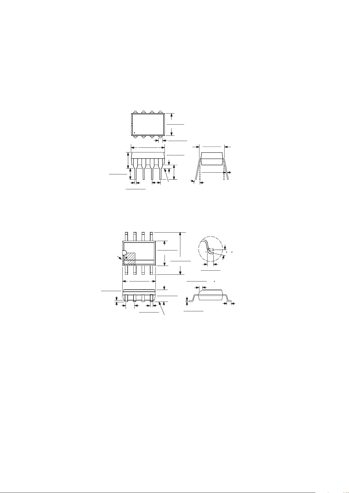
OUTLINE DIMENSIONS
Dimensions shown in inches and (mm).
8-Lead PDIP Package
(N-8)
0.200 (5.05)
0.125 (3.18)
0.150
(3.81)
MIN
0.210
(5.33)
MAX
0.430 (10.92)
0.348 (8.84)
0.280 (7.11)
0.240 (6.10)
4
5
8
1
0.070 (1.77)
0.045 (1.15)
0.022 (0.558)
0.014 (0.356)
0.325 (8.25)
0.300 (7.62)
0 - 15
0.100
(2.54)
BSC
0.015 (0.381)
0.008 (0.204)
SEATING
PLANE
0.060 (1.52)
0.015 (0.38)
8-Lead SOIC Package
(R-8)
SEATING
PLANE
SEE DETAIL
ABOVE
4
5
8
1
0.0688 (1.75)
0.0532 (1.35)
0.0098 (0.25)
0.0075 (0.19)
0.1574 (4.00)
0.1497 (3.80)
0.2440 (6.20)
0.2284 (5.80)
0.1968 (5.00)
0.1890 (4.80)
0.0192 (0.49)
0.0138 (0.35)
0.0500
(1.27)
BSC
0.0098 (0.25)
0.0040 (0.10)
× 45
0.0196 (0.50)
0.0099 (0.25)
0.0500 (1.27)
0.0160 (0.41)
PIN 1
0
- 8

REV. A
OP285
–15–
Revision History
Location Page
Data Sheet changed from REV. 0 to REV. A.
Edits to ORDERING GUIDE . . . . . . . . . . . . . . . . . . . . . . . . . . . . . . . . . . . . . . . . . . . . . . . . . . . . . . . . . . . . . . . . . . . . . . . . . . . . . . 3
Deleted WAFER TEST LIMITS . . . . . . . . . . . . . . . . . . . . . . . . . . . . . . . . . . . . . . . . . . . . . . . . . . . . . . . . . . . . . . . . . . . . . . . . . . . 3
Deleted DICE CHARACTERISTICS . . . . . . . . . . . . . . . . . . . . . . . . . . . . . . . . . . . . . . . . . . . . . . . . . . . . . . . . . . . . . . . . . . . . . . . 3

–16–
C00306–0–1/02
(A)
PRINTED IN U.S.A.
 Loading...