Dual 9 MHz Precision
8
7
6
5
V+
–IN B
+IN B
OUT B
1
2
3
4
–IN A
+IN A
V–
OUT A
+–
+–
OP285
www.BDTIC.com/ADI
a
FEATURES
Low Offset Voltage: 250 V
Low Noise: 6 nV/√ Hz
Low Distortion: 0.0006%
High Slew Rate: 22 V/s
Wide Bandwidth: 9 MHz
Low Supply Current: 5 mA
Low Offset Current: 2 nA
Unity-Gain Stable
SO-8 Package
APPLICATIONS
High Performance Audio
Active Filters
Fast Amplifiers
Integrators
GENERAL DESCRIPTION
The OP285 is a precision high-speed amplifier featuring the
Butler Amplifier front-end. This new front-end design combines the accuracy and low noise performance of bipolar
transistors with the speed of JFETs. This yields an amplifier
with high slew rates, low offset and good noise performance
at low supply currents. Bias currents are also low compared
to bipolar designs.
The OP285 offers the slew rate and low power of a JFET
amplifier combined with the precision, low noise and low
drift of a bipolar amplifier. Input offset voltage is laser-trimmed
and guaranteed less than 250 µV. This makes the OP285 useful
in dc-coupled or summing applications without the need for
special selections or the added noise of additional offset
adjustment circuitry. Slew rates of 22 V/µs and a bandwidth
of 9 MHz make the OP285 one of the most accurate medium
speed amplifiers available.
Operational Amplifier
OP285
PIN CONNECTIONS
8-Lead Narrow-Body SO (S-Suffix)
OUT A
1
–IN A
2
OP285
3
4
TOP VIEW
(Not to Scale)
+IN A
V–
8-Lead Epoxy DIP (P-Suffix)
The combination of low noise, speed and accuracy can be used
to build high speed instrumentation systems. Circuits such as
instrumentation amplifiers, ramp generators, bi-quad filters and
dc-coupled audio systems are all practical with the OP285. For
applications that require long term stability, the OP285 has a
guaranteed maximum long term drift specification.
The OP285 is specified over the XIND—extended industrial—
(–40°C to +85°C) temperature range. OP285s are available in
8-pin plastic DIP and SOIC-8 surface mount packages.
8
7
6
5
V+
OUT B
–IN B
+IN B
*
*Patents pending
REV. A
Information furnished by Analog Devices is believed to be accurate and
reliable. However, no responsibility is assumed by Analog Devices for its
may result from its use. No license is granted by implication or otherwise
under any patent or patent rights of Analog Devices.
use, nor for any infringements of patents or other rights of third parties that
One Technology Way, P.O. Box 9106, Norwood, MA 02062-9106, U.S.A.
Tel: 781/329-4700 www.analog.com
Fax: 781/326-8703 © Analog Devices, Inc., 2001

OP285–SPECIFICATIONS
www.BDTIC.com/ADI
(@ Vs = 15.0 V, TA = 25C, unless otherwise noted.)
Parameter Symbol Conditions Min Typ Max Unit
INPUT CHARACTERISTICS
Offset Voltage V
Input Bias Current I
Input Offset Current I
Input Voltage Range V
OS
V
OS
B
I
B
OS
I
OS
CM
Common-Mode Rejection CMRR V
Large-Signal Voltage Gain A
VO
A
VO
A
VO
–40°C ≤ TA ≤ +85°C 600 µV
VCM = 0 V 100 350 nA
VCM = 0 V, –40°C ≤ TA ≤ +85°C 400 nA
VCM = 0 V 2 ±50 nA
VCM = 0 V, –40°C ≤ TA ≤ +85°C2±100 nA
–10.5 10.5 V
= ±10.5 V,
CM
–40°C ≤ T
≤ +85°C 80 106 dB
A
RL = 2 kΩ 250 V/mV
RL = 2 kΩ, –40°C ≤ TA ≤ +85°C 175 V/mV
RL = 600 Ω 200 V/mV
35 250 µV
Common-Mode Input Capacitance 7.5 pF
Differential Input Capacitance 3.7 pF
Long-Term Offset Voltage ∆V
Offset Voltage Drift ∆V
OS
/∆T1µV/°C
OS
Note 1 300 µV
OUTPUT CHARACTERISTICS
Output Voltage Swing V
O
V
O
RL = 2 kΩ –13.5 +13.9 +13.5 V
RL = 2 kΩ, –40°C ≤ TA ≤ +85°C –13 +13.9 +13 V
RL = 600 Ω, V
= ±18 V –16/+14 V
S
POWER SUPPLY
Power Supply Rejection Ratio PSRR V
PSRR V
Supply Current I
SY
I
SY
= ±4.5 V to ±18 V 85 111 dB
S
= ±4.5 V to ±18 V,
S
–40°C ≤ T
≤ +85°C80 dB
A
VS = ±4.5 V to ±18 V, VO = 0 V,
R
= x, –40°C ≤ TA ≤ +85°C45mA
L
VS = ±22 V, VO, = 0 V, RL = x
–40°C ≤ T
≤ +85°C 5.5 mA
A
Supply Voltage Range VS ±4.5 ± 22 V
DYNAMIC PERFORMANCE
Slew Rate SR R
= 2 kΩ 15 22 V/µs
L
Gain Bandwidth Product GBP 9 MHz
Phase Margin o 62 Degrees
Settling Time t
s
t
s
Distortion A
Voltage Noise Density e
Current Noise Density i
n
e
n
n
To 0.1%, 10 V Step 625 ns
To 0.01%, 10 V Step 750 ns
= 1, V
V
f = 1 kHz, R
= 8.5 V p-p,
OUT
= 2 kΩ –104 dB
L
f = 30 Hz 7 nV/√Hz
f = 1 kHz 6 nV/√Hz
f = 1 kHz 0.9 pA/√Hz
Headroom THD + Noise ≤ 0.01%,
RL = 2 kΩ, VS = ±18 V >12.9 dBu
NOTE
1
Long-term offset voltage is guaranteed by a 1,000 hour life test performed on three independent wafer lots at 125 °C, with an LTPD of 1.3.
Specifications subject to change without notice.
–2–
REV. A

OP285
www.BDTIC.com/ADI
ABSOLUTE MAXIMUM RATINGS
Supply Voltage . . . . . . . . . . . . . . . . . . . . . . . . . . . . . . . . ±22 V
Input Voltage
Differential Input Voltage
2
. . . . . . . . . . . . . . . . . . . . . . . . . . . . . . . . ±18 V
2
. . . . . . . . . . . . . . . . . . . . . . ±7.5 V
Output Short-Circuit Duration to Gnd
Storage Temperature Range
P, S Package . . . . . . . . . . . . . . . . . . . . . . . –65°C to +150°C
Operating Temperature Range
OP285G . . . . . . . . . . . . . . . . . . . . . . . . . . . –40°C to +85°C
Junction Temperature Range
P, S Package . . . . . . . . . . . . . . . . . . . . . . . –65°C to +150°C
1
3
. . . . . . . . . Indefinite
Package Type
8-Pin Plastic DIP (P) 103 43 °C/W
8-Pin SOIC (S) 158 43 °C/W
NOTES
1
Absolute Maximum Ratings apply to packaged parts, unless otherwise noted.
2
For supply voltages less than ± 7.5 V, the absolute maximum input voltage is
equal to the supply voltage.
3
Shorts to either supply may destroy the device. See data sheet for full details.
4
JA is specified for the worst case conditions, i.e., JA is specified for device in
socket for cerdip, P-DIP, and LCC packages; JA is specified for device soldered
in circuit board for SOIC package.
Lead Temperature Range (Soldering 60 Sec) . . . . . . . . 300°C
ORDERING GUIDE
Temperature Package Package
Model Range Description Option
OP285GP* –40°C to +85°C 8-Pin Plastic DIP N-8
OP285GS –40°C to +85°C 8-Pin SOIC S0-8
OP285GSR –40°C to +85°C S0-8 Reel, 2500 pcs.
*Not for new designs. Obsolete April 2002.
CAUTION
ESD (electrostatic discharge) sensitive device. Electrostatic charges as high as 4000 V readily
accumulate on the human body and test equipment and can discharge without detection. Although
the OP285 features proprietary ESD protection circuitry, permanent damage may occur on devices
subjected to high-energy electrostatic discharges. Therefore, proper ESD precautions are
recommended to avoid performance degradation or loss of functionality.
4
JA
WARNING!
JC
ESD SENSITIVE DEVICE
Unit
REV. A
–3–

OP285
www.BDTIC.com/ADI
25
T
= 25C
A
20
R
= 2k
L
15
10
5
0
–5
–10
–15
OUTPUT VOLTAGE SWING – V
–20
–25
0 5 10 15 20 25
SUPPLY VOLTAGE – V
+VOM
–VOM
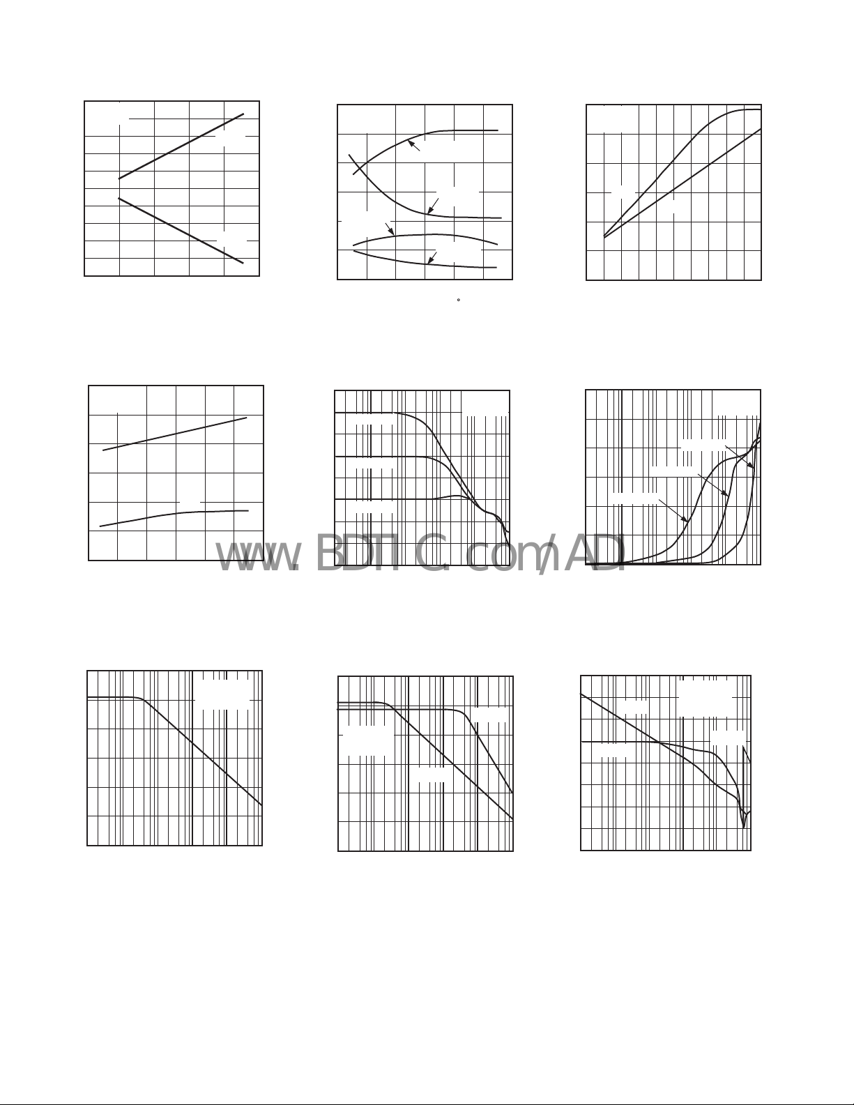
TPC 1. Output Voltage Swing vs.
Supply Voltage
50
VS = 15V
VS = 15V
R
= 2k
R
= 2k
L
L
45
40
35
30
SLEW RATE – V/s
25
20
TEMPERATURE – C
–SR
+SR
0
100–25–50 755025
TPC 4. Slew Rate vs. Temperature
1500
VS = 15V
V
= 10V
O
1250
1000
750
500
OPEN-LOOP GAIN – V/MV
250
0
–50
R
+GAIN
= 600
L
–25
+GAIN
= 2k
R
L
–GAIN
= 2k
R
L
–GAIN
= 600
R
L
0
TEMPERATURE – C
755025
TPC 2. Open-Loop Gain
vs. Temperature
CLOSED-LOOP GAIN – dB
–10
–20
–30
50
40
30
20
10
0
= +100
A
VCL
= +10
A
VCL
A
= +1
VCL
1k
10k 100k 1M 10M 100M
FREQUENCY – Hz
VS = 15V
= +25C
T
A
TPC 5. Closed-Loop Gain
vs. Frequency
100
30
VS = 15V
R
= 2k
L
25
20
15
+SR
–SR
10
SLEW RATE – V/s
5
0
0
DIFFERENTIAL INPUT VOLTAGE – V
1.0
0.80.60.40.2
TPC 3. Slew Rate vs. Differential
Input Voltage
60
50
40
A
= +10
30
A
VCL
20
IMPEDANCE –
10
0
100
1k 10k 100k 1M 10M
VCL
= +100
FREQUENCY – Hz
VS = 15V
= 25C
T
A
A
= +1
VCL
TPC 6. Closed-Loop Output Imped
ance vs. Frequency
120
= 15V
V
S
= 25C
T
A
COMMON MODE REJECTION – dB
100
80
60
40
20
0
100
1k 10k 100k 1M 10M
FREQUENCY – Hz
TPC 7. Common-Mode Rejection
vs. Frequency
120
100
VS = 15V
80
= 25C
T
A
60
40
20
POWER SUPPLY REJECTION – dB
0
10
100 1k 10k 100k 1M
FREQUENCY – Hz
TPC 8. Power Supply Rejection
vs. Frequency
–4–
–PSRR
+PSRR
100
80
60
– dB
40
MIN
PHASE
20
0
OPEN-LOOP G
–20
–40
–60
1k
GAIN
10k 100k 1M 10M 100M
FREQUENCY – Hz
V
= 15V
S
= 2k
R
L
T
= 25C
A
0
= 58
N
TPC 9. Open-Loop Gain, Phase
vs. Frequency
REV. A
0
45
90
135
180
225
270
PHASE – Degrees

Typical Performance Characteristics–OP285
www.BDTIC.com/ADI
11
10
9
8
GAIN BANDWIDTH PRODUCT – MHz
7
–25 755025
–50 100
TEMPERATURE – C
GBW
0
ø
M
65
60
55
50
40
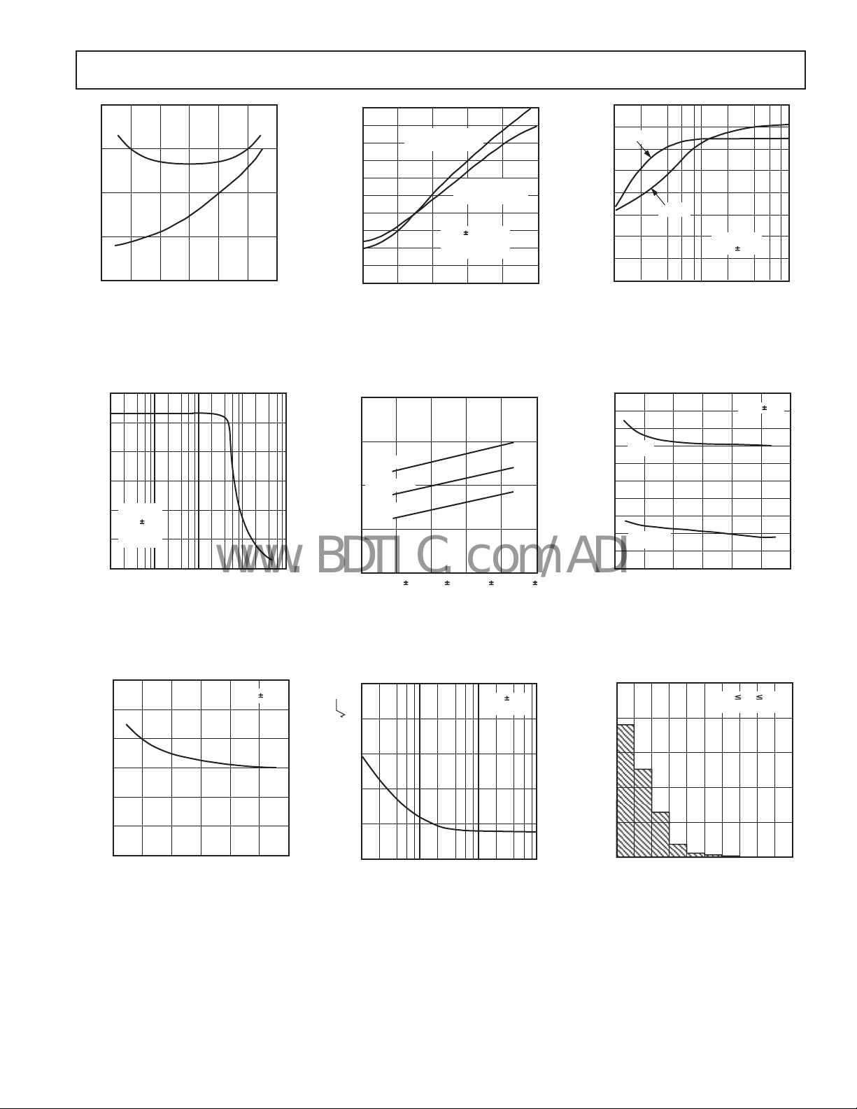
TPC 10. Gain Bandwidth Product,
Phase Margin vs. Temperature
30
25
20
15
10
TA = 25C
= 15V
V
S
= +1
A
VCL
5
MAXIMUM OUTPUT SWING – V
R
= 2k
L
0
1k
10k 10M1M100k
FREQUENCY – Hz
TPC 13. Maximum Output Swing
vs. Frequency
100
PHASE MARGIN – Degrees
90
80
70
60
50
40
OVERSHOOT – %
30
20
10
0
0
A = +1
VCL
NEGATIVE EDGE
A = +1
VCL
POSITIVE EDGE
VS = 15V
= 2k
R
L
= 100mV p-p
V
IN
100
LOAD CAPACITANCE – pF
300
TPC 11. Small-Signal Overshoot vs.|
Load Capacitance
5.0
4.5
TA = +85C
4.0
TA = +25C
TA = –40C
3.5
SUPPLY CURRENT – mA
3.0
0
5
SUPPLY VOLTAGE – V
TPC 14. Supply Current vs.
Supply Voltage
16
14
–VOM
12
10
8
6
4
2
MAXIMUM OUTPUT SWING – Volts
0
500
400200
100 1k 10k
+VOM
TA = 25C
= 15V
V
S
LOAD RESISTANCE –
TPC 12. Maximum Output Voltage
vs. Load Resistance
120
110
100
90
SINK
80
70
60
50
40
SOURCE
30
ABSOLUTE OUTPUT CURRENT – mA
20
1510
25
–50
0
–25
TEMPERATURE – C
VS = 15V
7525 50
100
TPC 15. Short Circuit Current vs.
Temperature
300
VS = 15V
250
200
150
100
INPUT BIAS CURRENT – nA
50
0
–25
–50
0
TEMPERATURE – C
755025
TPC 16. Input Bias Current vs.
Temperature
100
5
Hz
4
3
2
1
CURRENT NOISE DENSITY – pA/
10
100 100k1k
FREQUENCY – Hz
TPC 17. Current Noise Density vs.
Frequency
REV. A
–5–
VS = 15V
T
= 25C
A
250
–40C TA +85C
TC V
402 OP AMPS
– V/ C
OS
200
150
UNITS
100
50
0
0
1
TPC 18. tC VOS Distribution
10
98765432
 Loading...