Precision Rail-to-Rail
A
T
2
O
www.BDTIC.com/ADI
Input and Output Operational Amplifiers
FEATURES
Single-supply operation
Wide bandwidth: 4 MHz
Low offset voltage: 65 μV
Unity-gain stable
High slew rate: 4.0 V/μs
Low noise: 3.9 nV/√Hz
APPLICATIONS
Battery-powered instrumentation
Power supply control and protection
Telecommunications
DAC output amplifier
ADC input buffer
GENERAL DESCRIPTION
The OP184/OP284/OP484 are single, dual, and quad single-supply,
4 MHz bandwidth amplifiers featuring rail-to-rail inputs and
outputs. They are guaranteed to operate from 3 V to 36 V (or
±1.5 V to ±18 V).
These amplifiers are superb for single-supply applications requiring
both ac and precision dc performance. The combination of wide
bandwidth, low noise, and precision makes the OP184/OP284/
OP484 useful in a wide variety of applications, including filters
and instrumentation.
Other applications for these amplifiers include portable telecommunications equipment, power supply control and protection,
and use as amplifiers or buffers for transducers with wide output
ranges. Sensors requiring a rail-to-rail input amplifier include
Hall effect, piezoelectric, and resistive transducers.
The ability to swing rail-to-rail at both the input and output
enables designers to build multistage filters in single-supply
systems and to maintain high signal-to-noise ratios.
The OP184/OP284/OP484 are specified over the hot extended
industrial temperature range of −40°C to +125°C. The single
OP184 is available in 8-lead SOIC surface mount packages. The
dual OP284 is available in 8-lead PDIP and SOIC surface mount
packages. The quad OP484 is available in 14-lead PDIP and
14-lead, narrow-body SOIC packages.
OP184/OP284/OP484
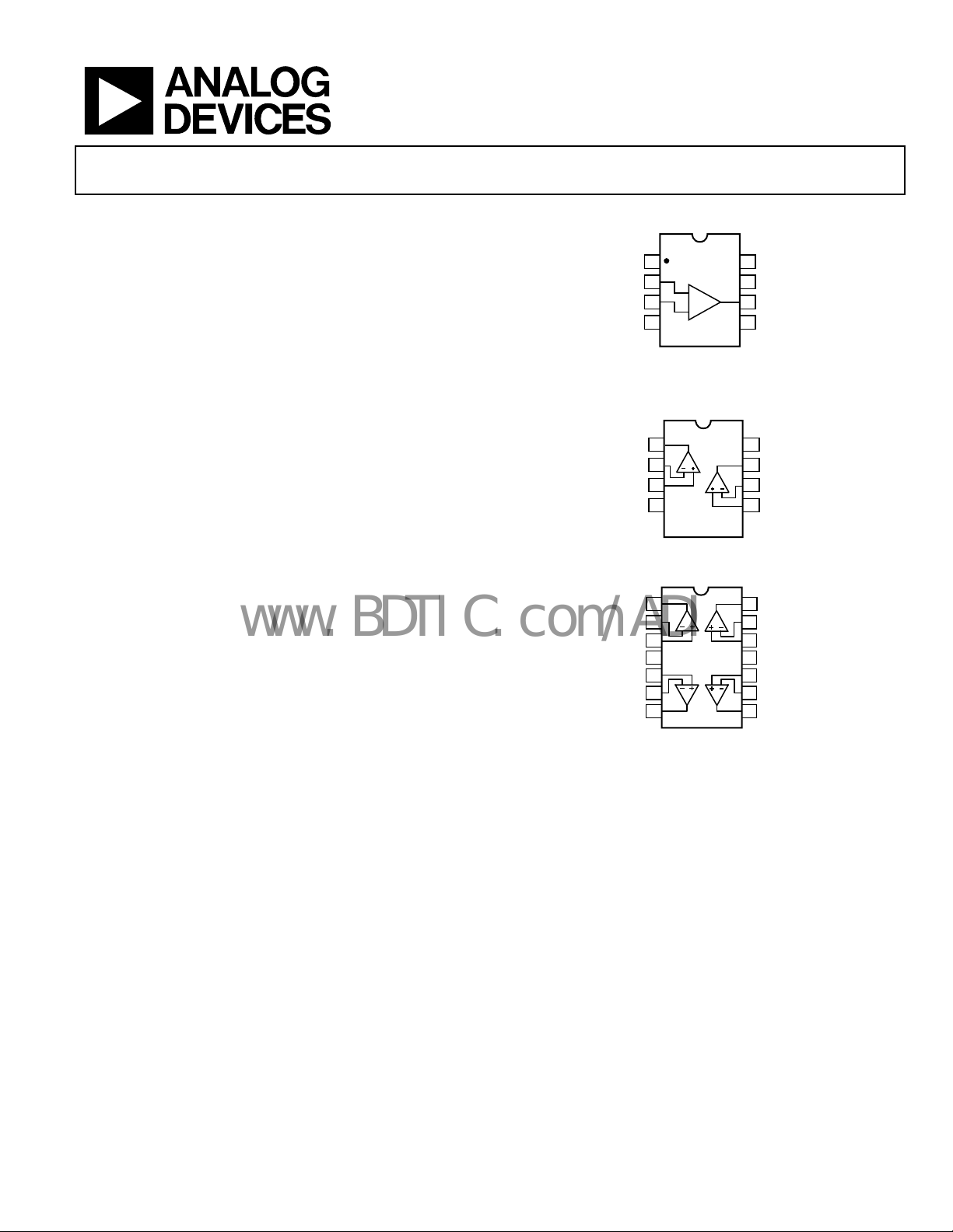
PIN CONFIGURATIONS
OP184
1
DNC
–IN A
2
–
3
+IN
V–
NOTES
1. NC = NO CONNEC
. DNC = DO NOT CO NNECT
4
(Not to Scale)
+
TOP VIEW
Figure 1. 8-Lead SOIC (S-Suffix)
OP284
1
UT A
2
–IN A
3
+IN A
4
V–
TOP VIEW
(Not to Scale)
Figure 2. 8-Lead PDIP (P-Suffix)
8-Lead SOIC (S-Suffix)
1
OUT A
2
–IN A
3
+IN A
V+
+IN B
–IN B
OUT B
4
TOP VIEW
(Not to Scale)
5
6
7
OP484
Figure 3. 14-Lead PDIP (P-Suffix)
14-Lead Narrow-Body SOIC (S-Suffix)
8
7
6
5
14
13
12
11
10
8
7
6
5
9
8
NC
V+
OUT A
DNC
V+
OUT B
–IN B
+IN B
OUT D
–IN D
+IN D
V–
+IN C
–IN C
OUT C
00293-001
00293-002
00293-003
Rev. F
Information furnished by Analog Devices is believed to be accurate and reliable. However, no
responsibility is assumed by Analog Devices for its use, nor for any infringements of patents or other
rights of third parties that may result from its use. Specifications subject to change without notice. No
license is granted by implication or otherwise under any patent or patent rights of Analog Devices.
Trademarks and registered trademarks are the property of their respective owners.
One Technology Way, P.O. Box 9106, Norwood, MA 02062-9106, U.S.A.
Tel: 781.329.4700 www.analog.com
Fax: 781.461.3113 ©1996–2008 Analog Devices, Inc. All rights reserved.

OP184/OP284/OP484
www.BDTIC.com/ADI
TABLE OF CONTENTS
Features .............................................................................................. 1
Applications ....................................................................................... 1
General Description ......................................................................... 1
Pin Configurations ........................................................................... 1
Revision History ............................................................................... 2
Specifications ..................................................................................... 3
Electrical Characteristics ............................................................. 3
Absolute Maximum Ratings ............................................................ 6
Thermal Resistance ...................................................................... 6
ESD Caution .................................................................................. 6
Typical Performance Characteristics ............................................. 7
Applications Information .............................................................. 14
Functional Description .............................................................. 14
Input Overvoltage Protection ................................................... 14
REVISION HISTORY
9/08—Rev. E to Rev. F
Changes to General Description .................................................... 1
Changes to Figure 4 .......................................................................... 6
Changes to Low Dropout Regulator with Current Limiting .... 20
7/08—Rev. D to Rev. E
Changes to Figure 1 .......................................................................... 1
Changes to Figure 12 ........................................................................ 8
Changes to Figure 36 and Figure 37 ............................................. 12
Changes to Designing Low Noise Circuits in Single-Supply
Applications Section ....................................................................... 15
Updated Outline Dimensions ....................................................... 21
Changes to Ordering Guide .......................................................... 22
4/06—Rev. C to Rev. D
Changes to Table 1 ............................................................................ 3
Changes to Table 2 ............................................................................ 4
Changes to Table 3 ............................................................................ 5
Deleted Reference to 1993 System Applications Guide............... 15
Output Phase Reversal ............................................................... 15
Designing Low Noise Circuits in Single-Supply
Applications ................................................................................ 15
Overdrive Recovery ................................................................... 16
Single-Supply, 3 V Instrumentation Amplifier ...................... 16
2.5 V Reference from a 3 V Supply .......................................... 17
5 V Only, 12-Bit DAC Swings Rail-to-Rail ............................. 17
High-Side Current Monitor ...................................................... 18
Capacitive Load Drive Capability ............................................ 18
Low Dropout Regulator with Current Limiting ..................... 18
3 V, 50 Hz/60 Hz Active Notch Filter with False Ground ..... 20
Outline Dimensions ....................................................................... 21
Ordering Guide .......................................................................... 22
3/06—Rev. B to Rev. C
Changes to Figure 1 Caption........................................................... 1
Changes to Table 1 ............................................................................ 3
Changes to Table 2 ............................................................................ 4
Changes to Table 3 ............................................................................ 5
Changes to Table 4 ............................................................................ 6
Changes to Figure 5 through Figure 9 ........................................... 7
Changes to Functional Description Section ............................... 14
Deleted SPICE Macro Model ........................................................ 21
Updated Outline Dimensions ....................................................... 21
Changes to Ordering Guide .......................................................... 22
9/02—Rev. A to Rev. B
Changes to Pin Configurations ...................................................... 1
Changes to Specifications, Input Bias Current Maximum.......... 2
Changes to Ordering Guide ............................................................ 5
Updated Outline Dimensions ....................................................... 19
6/02—Rev. 0 to Rev. A
10/96—Revision 0: Initial Version
Rev. F | Page 2 of 24
OP184/OP284/OP484
www.BDTIC.com/ADI
SPECIFICATIONS
ELECTRICAL CHARACTERISTICS
VS = 5.0 V, VCM = 2.5 V, TA = 25°C, unless otherwise noted.
Table 1.
Parameter Symbol Conditions Min Typ Max Unit
INPUT CHARACTERISTICS
Offset Voltage, OP184/OP284E Grade1VOS 65 V
−40°C ≤ TA ≤ +125°C 165 V
Offset Voltage, OP184/OP284F Grade
−40°C ≤ TA ≤ +125°C 350 V
Offset Voltage, OP484E Grade
–40°C ≤ TA ≤ +125°C 175 V
Offset Voltage, OP484F Grade
–40°C ≤ TA ≤ +125°C 450 V
Input Bias Current IB 60 450 nA
–40°C ≤ TA ≤ +125°C 600 nA
Input Offset Current IOS 2 50 nA
–40°C ≤ TA ≤ +125°C 50 nA
Input Voltage Range 0 5 V
Common-Mode Rejection Ratio CMRR VCM = 0 V to 5 V 60 dB
V
Large Signal Voltage Gain AVO RL = 2 kΩ, 1 V ≤ VO ≤ 4 V 50 240 V/mV
R
Bias Current Drift ∆IB/∆T 150 pA/°C
OUTPUT CHARACTERISTICS
Output Voltage High VOH IL = 1.0 mA 4.85 V
Output Voltage Low VOL IL = 1.0 mA 125 mV
Output Current I
POWER SUPPLY
Power Supply Rejection Ratio PSRR VS = 2.0 V to 10 V, −40°C ≤ TA ≤ +125°C 76 dB
Supply Current/Amplifier ISY VO = 2.5 V, −40°C ≤ TA ≤ +125°C 1.45 mA
Supply Voltage Range VS 3 36 V
DYNAMIC PERFORMANCE
Slew Rate SR RL = 2 kΩ 1.65 2.4 V/µs
Settling Time tS To 0.01%, 1.0 V step 2.5 µs
Gain Bandwidth Product GBP 3.25 MHz
Phase Margin ΦM 45 Degrees
NOISE PERFORMANCE
Voltage Noise en p-p 0.1 Hz to 10 Hz 0.3 V p-p
Voltage Noise Density en f = 1 kHz 3.9 nV/√Hz
Current Noise Density in 0.4 pA/√Hz
1
Input offset voltage measurements are performed by automated test equipment approximately 0.5 seconds after application of power.
1
V
1
V
1
V
125 V
OS
75 V
OS
150 V
OS
= 1.0 V to 4.0 V, −40°C ≤ TA ≤ +125°C 86 dB
CM
= 2 kΩ, −40°C ≤ TA ≤ +125°C 25 V/mV
L
±6.5 mA
OUT
Rev. F | Page 3 of 24
OP184/OP284/OP484
www.BDTIC.com/ADI
VS = 3.0 V, VCM = 1.5 V, TA = 25°C, unless otherwise noted.
Table 2.
Parameter Symbol Conditions Min Typ Max Unit
INPUT CHARACTERISTICS
Offset Voltage, OP184/OP284E Grade
−40°C ≤ TA ≤ +125°C 165 V
Offset Voltage, OP184/OP284F Grade
−40°C ≤ TA ≤ +125°C 350 V
Offset Voltage, OP484E Grade
–40°C ≤ TA ≤ +125°C 200 V
Offset Voltage, OP484F Grade
–40°C ≤ TA ≤ +125°C 450 V
Input Bias Current IB 60 450 nA
−40°C ≤ TA ≤ +125°C 600 nA
Input Offset Current IOS −40°C ≤ TA ≤ +125°C 50 nA
Input Voltage Range 0 3 V
Common-Mode Rejection Ratio CMRR VCM = 0 V to 3 V 60 dB
V
OUTPUT CHARACTERISTICS
Output Voltage High VOH IL = 1.0 mA 2.85 V
Output Voltage Low VOL IL = 1.0 mA 125 mV
POWER SUPPLY
Power Supply Rejection Ratio PSRR VS = ±1.25 V to ±1.75 V 76 dB
Supply Current/Amplifier ISY VO = 1.5 V, −40°C ≤ TA ≤ +125°C 1.35 mA
DYNAMIC PERFORMANCE
Gain Bandwidth Product GBP 3 MHz
NOISE PERFORMANCE
Voltage Noise Density en f = 1 kHz 3.9 nV/√Hz
1
Input offset voltage measurements are performed by automated test equipment approximately 0.5 seconds after application of power.
1
V
1
V
1
V
1
V
65 V
OS
125 V
OS
100 V
OS
150 V
OS
= 0 V to 3 V, −40°C ≤ TA ≤ +125°C 56 dB
CM
Rev. F | Page 4 of 24
OP184/OP284/OP484
www.BDTIC.com/ADI
VS = ±15.0 V, VCM = 0 V, TA = 25°C, unless otherwise noted.
Table 3.
Parameter Symbol Conditions Min Typ Max Unit
INPUT CHARACTERISTICS
Offset Voltage, OP184/OP284E Grade1VOS 100 V
−40°C ≤ TA ≤ +125°C 200 V
Offset Voltage, OP184/OP284F Grade
−40°C ≤ TA ≤ +125°C 375 V
Offset Voltage, OP484E Grade
−40°C ≤ TA ≤ +125°C 300 V
Offset Voltage, OP484F Grade
−40°C ≤ TA ≤ +125°C 500 V
Input Bias Current IB 80 450 nA
−40°C ≤ TA ≤ +125°C 575 nA
Input Offset Current IOS −40°C ≤ TA ≤ +125°C 50 nA
Input Voltage Range −15 +15 V
Common-Mode Rejection Ratio CMRR VCM = −14.0 V to +14.0 V, −40°C ≤ TA ≤ +125°C 86 90 dB
V
Large Signal Voltage Gain AVO R
R
Offset Voltage Drift E Grade ∆VOS/∆T 0.2 2.00 V/°C
Bias Current Drift ∆VB/∆T 150 pA/°C
OUTPUT CHARACTERISTICS
Output Voltage High VOH IL = 1.0 mA 14.8 V
Output Voltage Low VOL IL = 1.0 mA −14.875 V
Output Current I
POWER SUPPLY
Power Supply Rejection Ratio PSRR VS = ±2.0 V to ±18 V, −40°C ≤ TA ≤ +125°C 90 dB
Supply Current/Amplifier ISY VO = 0 V, −40°C ≤ TA ≤ +125°C 2.0 mA
Supply Current/Amplifier ISY V
DYNAMIC PERFORMANCE
Slew Rate SR RL = 2 kΩ 2.4 4.0 V/µs
Full-Power Bandwidth BWp 1% distortion, RL = 2 kΩ, VO = 29 V p-p 35 kHz
Settling Time tS To 0.01%, 10 V step 4 µs
Gain Bandwidth Product GBP 4.25 MHz
Phase Margin ΦM 50 Degrees
NOISE PERFORMANCE
Voltage Noise en p-p 0.1 Hz to 10 Hz 0.3 µV p-p
Voltage Noise Density en f = 1 kHz 3.9 nV/√Hz
Current Noise Density in 0.4 pA/√Hz
1
Input offset voltage measurements are performed by automated test equipment approximately 0.5 seconds after application of power.
1
V
1
V
1
V
175 V
OS
150 V
OS
250 V
OS
= −15.0 V to +15.0 V 80 dB
CM
= 2 kΩ, −10 V ≤ VO ≤ 10 V 150 1000 V/mV
L
= 2 kΩ, −40 V ≤ TA ≤ +125°C 75 V/mV
L
±10 mA
OUT
= ±18 V, −40°C ≤ TA ≤ +125°C 2.25 mA
S
Rev. F | Page 5 of 24
OP184/OP284/OP484
V
www.BDTIC.com/ADI
ABSOLUTE MAXIMUM RATINGS
Table 4.
Parameter Rating
Supply Voltage ±18 V
Input Voltage ±18 V
Differential Input Voltage1 ±0.6 V
Output Short-Circuit Duration to GND Indefinite
Storage Temperature Range
P-Suffix, S-Suffix Packages −65°C to +150°C
Operating Temperature Range
OP184/OP284/OP484E/OP484F −40°C to +125°C
Junction Temperature Range
P-Suffix, S-Suffix Packages −65°C to +150°C
Lead Temperature
(Soldering 60 sec)
1
For input voltages greater than 0.6 V, the input current should be limited to
less than 5 mA to prevent degradation or destruction of the input devices.
300°C
THERMAL RESISTANCE
θJA is specified for the worst-case conditions; that is, θJA is specified
for a device in socket for PDIP. θ
in the circuit board for SOIC packages.
Table 5. Thermal Resistance
Package Type θJA θ
8-Lead PDIP (P-Suffix) 103 43 °C/W
8-Lead SOIC (S-Suffix) 158 43 °C/W
14-Lead PDIP (P-Suffix) 83 39 °C/W
14-Lead SOIC (S-Suffix) 92 27 °C/W
ESD CAUTION
Stresses above those listed under Absolute Maximum Ratings
may cause permanent damage to the device. This is a stress
rating only; functional operation of the device at these or any
other conditions above those indicated in the operational
section of this specification is not implied. Exposure to absolute
maximum rating conditions for extended periods may affect
device reliability.
Absolute maximum ratings apply to both DICE and packaged
parts, unless otherwise noted.
RB1
TP
JB1
–IN +IN
QB2
N+CB1
P+M
QB1
JB2
Q1
R3
Q3
RB2
R1
QL1
QB3
QL2
R4
QB6
Q4
QB5
Q11
Q2
QB4
R2
Q7
Q9
Q5
CC1
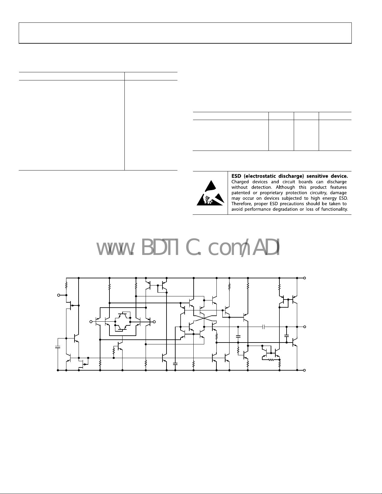
Figure 4. Simplified Schematic
Q12
Q8
Q10
Q6
QB7
R5
is specified for a device soldered
JA
Unit
JC
CC
RB3
QB9
R6
R7
QB8
RB4
QB10
CC2
FFC
Q14
Q13
R8
R11
Q15
C
R10
Q17
Q18
OUT
V
EE
00293-004
O
Q16
R9
Rev. F | Page 6 of 24
OP184/OP284/OP484
–
www.BDTIC.com/ADI
TYPICAL PERFORMANCE CHARACTERISTICS
300
VS= 3V
T
= 25°C
A
270
V
= 1.5V
CM
240
210
180
150
QUANTITY
120
90
60
30
0
–100 –75 –50 –25 0 25 50 75 100
INPUT OFFSET VOLTAGE (µV )
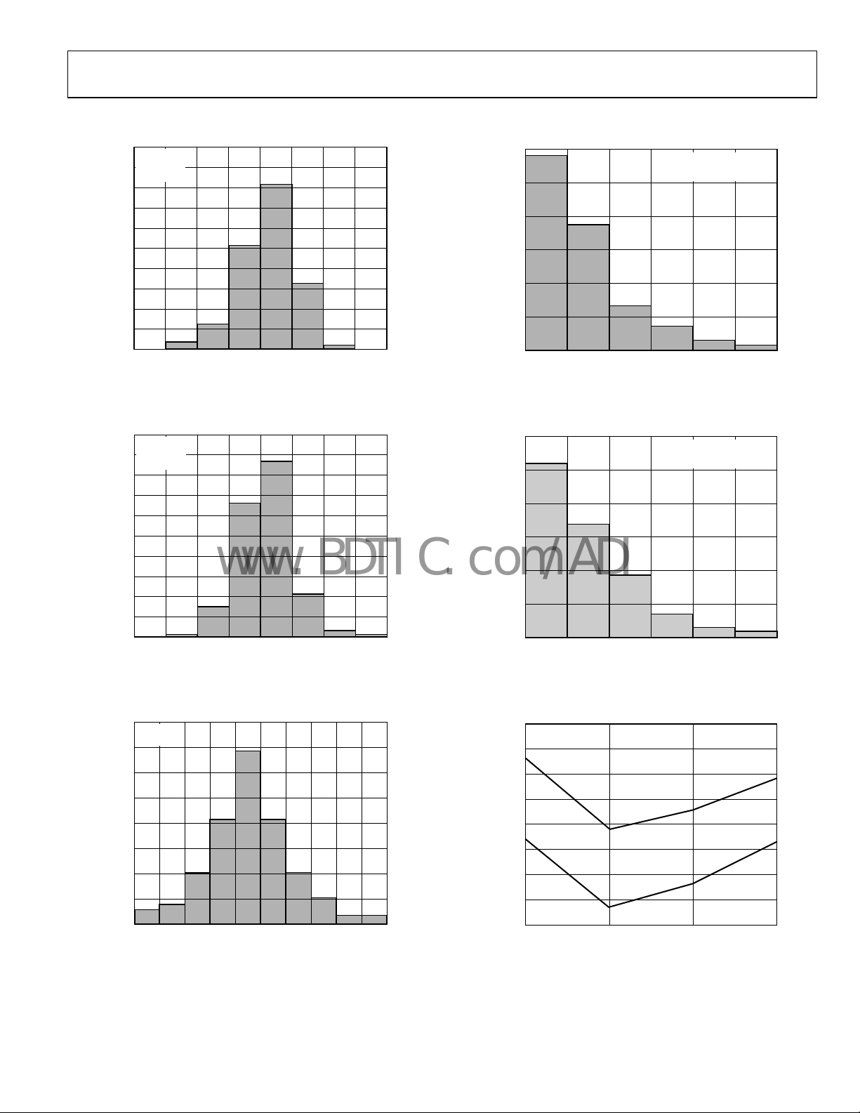
Figure 5. Input Offset Voltage Distribution
00293-005
300
250
200
150
QUANTITY
100
50
0
0 0.250.500.751.001.251.
OFFSET VO LTAGE DRIFT , TCVOS (µV/°C)
VS = 5V
–40°C ≤ T
≤ +125°C
A
Figure 8. Input Offset Voltage Drift Distribution
00293-008
50
300
VS= 5V
= 25°C
T
A
270
V
= 2.5V
CM
240
210
180
150
QUANTITY
120
90
60
30
0
–100 –75 –50 –25 0 25 50 75 100
INPUT OFFSET VOLTAGE (µV)
Figure 6. Input Offset Voltage Distribution
200
VS= ±15V
T
= 25°C
A
175
150
125
100
QUANTITY
75
300
250
200
150
QUANTITY
100
50
00293-006
0
0 0.250.500.751.001.251.
OFFSET VO LTAGE DRIFT , TCVOS (µV/°C)
VS = ±15V
–40°C ≤ T
≤ +125°C
A
00293-009
50
Figure 9. Input Offset Voltage Drift Distribution
–45
–50
–55
–60
–65
40
= +5V
V
S
= VS/2
V
CM
50
25
0
–125 –100 –75 –50 –25 0 25 10050 75 125
INPUT OFFSET VOLTAGE (µV)
00293-007
Figure 7. Input Offset Voltage Distribution
Rev. F | Page 7 of 24
–70
INPUT BIAS CURRENT (nA)
–75
–80
–40 25 85 125
V
= ±15V
S
TEMPERATURE (°C)
Figure 10. Bias Current vs. Temperature
00293-010
OP184/OP284/OP484
www.BDTIC.com/ADI
500
400
300
200
100
0
–100
–200
INPUT BIAS CURRENT (nA)
–300
–400
–500
–15 –10 –5 0 5 10 15
COMMON-MODE VOLTAGE (V)
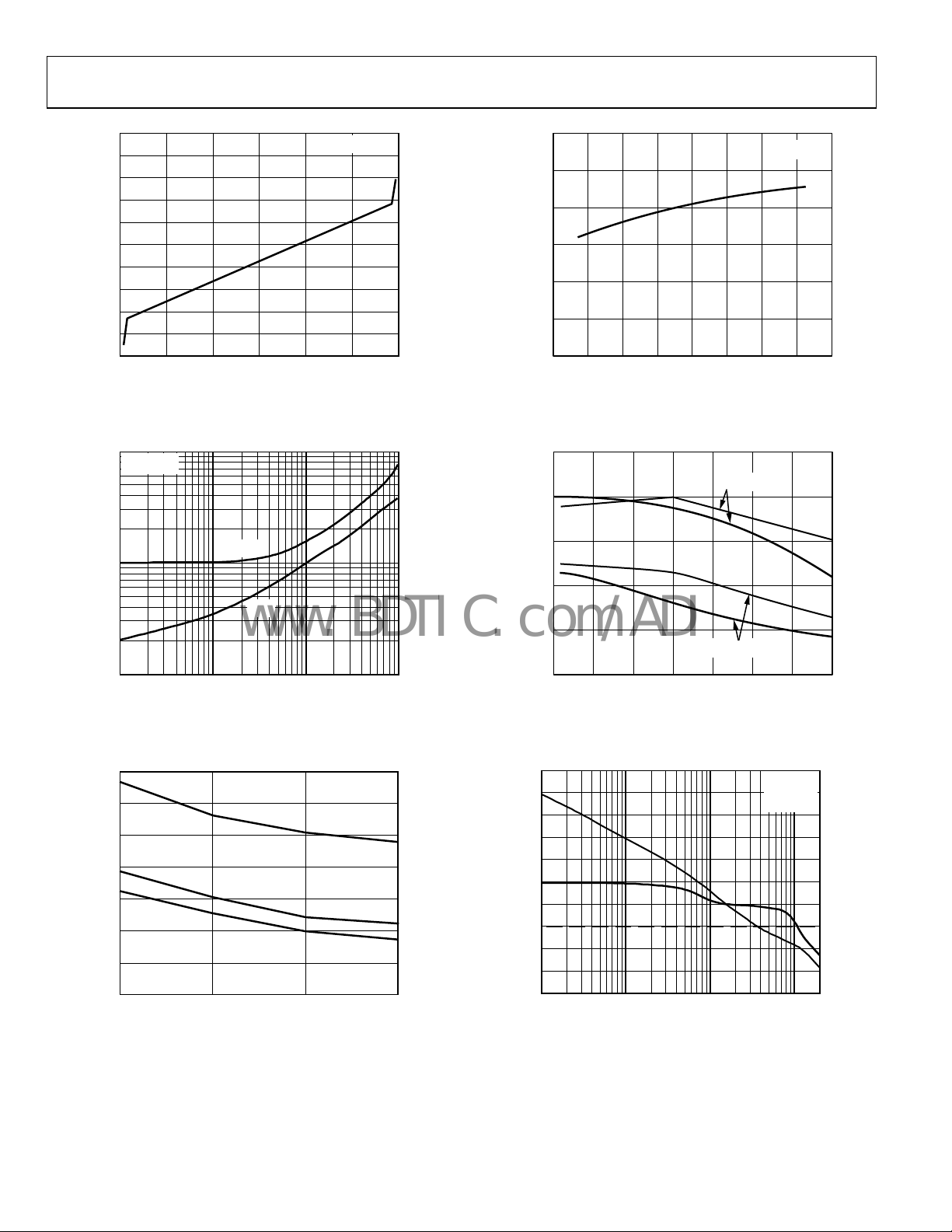
Figure 11. Input Bias Current vs. Common-Mode Voltage
VS = ±15V
00293-011
1.50
1.25
1.00
0.75
0.50
0.25
SUPPLY CURRENT/ PER AMPLIF IER (mA)
0
0 ±2. 5 ±5. 0 ±7. 5 ±10.0 ±12.5 ±15.0 ±17.5 ±20.0
SUPPLY VOLTAGE (V)
Figure 14. Supply Current vs. Supply Voltage
TA = 25°C
00293-014
1000
VS = ±15V
100
OUTPUT VOLTAGE (mV)
10
0.01 0.1 1 10
SOURCE
SINK
LOAD CURRENT (mA)
Figure 12. Output Voltage to Supply Rail vs. Load Current
1.2
1.1
1.0
0.9
0.8
0.7
SUPPLY CURRENT/ AMPLIFIER (mA)
0.6
0.5
–40 25 85 125
TEMPERATURE (°C)
VS = ±15V
V
= +5V
S
= +3V
V
S
Figure 13. Supply Current vs. Temperature
50
40
30
–I
SC
20
+I
SC
10
SHORT-CIRCUIT CURRENT (mA)
00293-012
0
–50 –25 0 25 50 75 100 125
TEMPERATURE (°C)
VS = ±15V
+I
SC
–I
SC
VS = +5V, VCM = +2.5V
00293-015
Figure 15. Short-Circuit Current vs. Temperature
70
60
50
40
30
20
10
0
OPEN-LOOP GAIN (dB)
–10
–20
00293-013
–30
10k 100k 1M 10M
FREQUENCY (Hz)
VS = 5V
T
= 25°C
A
NO LOAD
0
45
90
135
180
225
270
PHASE SHIFT (Degrees)
00293-016
Figure 16. Open-Loop Gain and Phase vs. Frequency (No Load)
Rev. F | Page 8 of 24
 Loading...