Quad 12-Bit Serial
Voltage Output DAC
DAC8420
FEATURES
Guaranteed Monotonic over Temperature
Excellent Matching between DACs
Unipolar or Bipolar Operation
Buffered Voltage Outputs
High Speed Serial Digital Interface
Reset to Zero Scale or Midscale
Wide Supply Range, +5 V Only to ⴞ15 V
Low Power Consumption (35 mW max)
Available in 16-Lead PDIP, CERDIP, and SOIC Packages
APPLICATIONS
Software Controlled Calibration
Servo Controls
Process Control and Automation
ATE
GENERAL DESCRIPTION
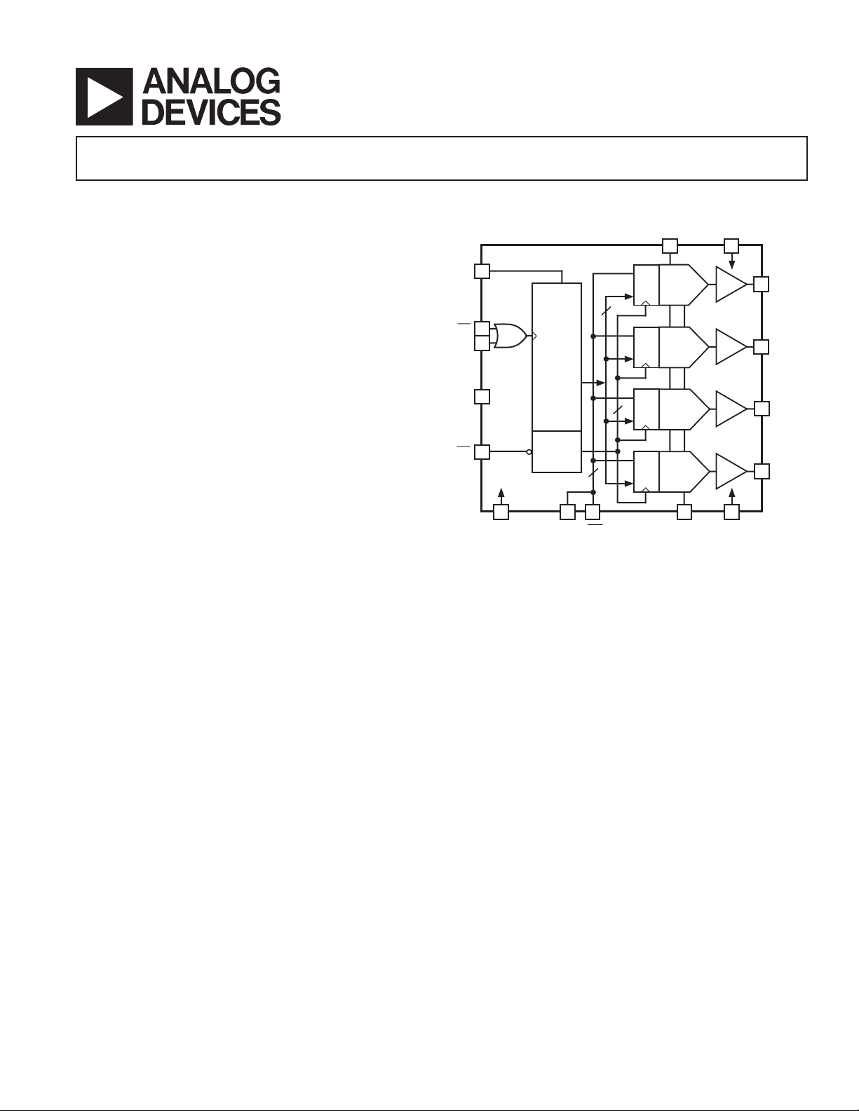
The DAC8420 is a quad, 12-bit voltage-output DAC with serial
digital interface in a 16-lead package. Utilizing BiCMOS technology, this monolithic device features unusually high circuit density
and low power consumption. The simple, easy-to-use serial digital
input and fully buffered analog voltage outputs require no external
components to achieve specified performance.
The 3-wire serial digital input is easily interfaced to microprocessors running at 10 MHz with minimal additional circuitry.
Each DAC is addressed individually by a 16-bit serial word
consisting of a 12-bit data word and an address header. The
user-programmable reset control CLR forces all four DAC
FUNCTIONAL BLOCK DIAGRAM
VDD
1
7
VOUTA
6
VOUTB
3
VOUTC
2
VOUTD
4
815169
SDI
CS
CLK
NC
LD
VREFHI
5
10
12
11
13
14
GND
SHIFT
REGISTER
DECODE
CLSEL
2
CLR
REG
REG
DAC A
A
A
12
REG
DAC B
B
REG
4
DAC C
C
REG
DAC D
D
VREFLO VSS
outputs to either zero scale or midscale, asynchronously overriding the current DAC register values. The output voltage range,
determined by the inputs VREFHI and VREFLO, is set by the
user for positive or negative unipolar or bipolar signal swings
within the supplies, allowing considerable design flexibility.
The DAC8420 is available in 16-lead PDIP, CERDIP, and
SOIC packages. Operation is specified with supplies ranging
from +5 V only to ±15 V, with references of +2.5 V to ±10 V,
respectively. Power dissipation when operating from ±15 V
supplies is less than 255 mW (max), and only 35 mW (max)
with a +5 V supply.
REV. A
Information furnished by Analog Devices is believed to be accurate and
reliable. However, no responsibility is assumed by Analog Devices for its
use, nor for any infringements of patents or other rights of third parties that
may result from its use. No license is granted by implication or otherwise
under any patent or patent rights of Analog Devices. Trademarks and
registered trademarks are the property of their respective owners.
One Technology Way, P.O. Box 9106, Norwood, MA 02062-9106, U.S.A.
Tel: 781/329-4700 www.analog.com
Fax: 781/326-8703 © 2003 Analog Devices, Inc. All rights reserved.
DAC8420–SPECIFICATIONS
1
ELECTRICAL CHARACTERISTICS
VSS = –5.0 V ⴞ 5%, V
= –2.5 V, –40ⴗC ≤ TA ≤ +85ⴗC, unless otherwise noted. See Note 2 for supply variations.)
VREFLO
(@ VDD = +5.0 V ⴞ 5%, VSS = 0.0 V, V
= +2.5 V, V
VREFHI
= 0.0 V, and
VREFLD
Parameter Symbol Condition Min Typ Max Unit
STATIC ACCURACY
Integral Linearity E Grade INL ±1/4 ±1 LSB
Integral Linearity E Grade INL Note 3, V
= 0 V ±1/2 ±3 LSB
SS
Integral Linearity F Grade INL ± 3/4 ± 2 LSB
Integral Linearity F Grade INL Note 3, V
= 0 V ±1 ±4 LSB
SS
Differential Linearity DNL Monotonic over Temperature ±1/4 ±1 LSB
Zero-Scale Error ZSE R
Full-Scale Error FSE R
Zero-Scale Error ZSE Note 3, R
Full-Scale Error FSE Note 3, R
Zero-Scale Tempco TC
Full-Scale Tempco TC
ZSE
FSE
= 2 kΩ, VSS = –5 V ±4 LSB
L
= 2 kΩ, VSS = –5 V ±4 LSB
L
= 2 kΩ, VSS = 0 V ±8 LSB
L
= 2 kΩ, VSS = 0 V ±8 LSB
L
Note 4, RL = 2 kΩ, VSS = –5 V ±10 ppm/°C
Note 4, RL = 2 kΩ, VSS = –5 V ±10 ppm/°C
MATCHING PERFORMANCE
Linearity Matching ±1 LSB
REFERENCE
Positive Reference Input Range V
Negative Reference Input Range V
Negative Reference Input Range V
Reference High Input Current I
Reference Low Input Current I
VREFHI
VREFLO
VREFLO
VREFHI
VREFLO
Note 5 V
Note 5 V
Note 5, VSS = 0 V 0 V
Codes 0x000, 0x555 –0.75 ±0.25 +0.75 mA
Codes 0x000, 0x555, VSS = –5 V –1.0 –0.6 mA
+ 2.5 VDD – 2.5 V
VREFLO
SS
V
VREFHI
VREFHI
– 2.5 V
– 2.5 V
AMPLIFIER CHARACTERISTICS
Output Current I
Settling Time t
OUT
S
VSS = –5 V –1.25 +1.25 mA
To 0.01%, Note 6 8 µs
Slew Rate SR 10% to 90%, Note 6 1.5 V/µs
LOGIC CHARACTERISTICS
Logic Input High Voltage V
Logic Input Low Voltage V
Logic Input Current I
Input Capacitance C
LOGIC TIMING CHARACTERISTICS
Data Setup Time t
Data Hold t
Clock Pulse Width High t
Clock Pulse Width Low t
Select Time t
Deselect Delay t
Load Disable Time t
Load Delay t
Load Pulse Width t
Clear Pulse Width t
4, 7
INH
INL
IN
IN
DS
DH
CH
CL
CSS
CSH
LD1
LD2
LDW
CLRW
Note 4 13 pF
2.4 V
0.8 V
10 µA
25 ns
55 ns
90 ns
120 ns
90 ns
5ns
130 ns
35 ns
80 ns
150 ns
SUPPLY CHARACTERISTICS
Power Supply Sensitivity PSRR 0.002 0.01 %/%
Positive Supply Current I
Negative Supply Current I
Power Dissipation P
NOTES
1
Typical values indicate performance measured at 25°C.
2
All supplies can be varied ± 5% and operation is guaranteed. Device is tested with VDD = 4.75 V.
3
For single-supply operation (V
4
Guaranteed but not tested.
5
Operation is guaranteed over this reference range, but linearity is neither tested nor guaranteed.
6
V
swing between +2.5 V and –2.5 V with VDD = 5.0 V.
OUT
7
All input control signals are specified with tr = tf = 5 ns (10% to 90% of 5 V) and timed from a voltage level of 1.6 V.
Specifications subject to change without notice.
= 0 V, VSS = 0 V), due to internal offset errors INL and DNL are measured beginning at code 0x003.
VREFLO
DD
SS
DISS
–6 –3 mA
VSS = 0 V 20 35 mW
47 mA
REV. A–2–
DAC8420
1
ELECTRICAL CHARACTERISTICS
V
= –10.0 V, –40ⴗC ≤ TA ≤ +85ⴗC, unless otherwise noted. See Note 2 for supply variations.)
VREFLO
(@ VDD = +15.0 V ⴞ 5%, VSS = –15.0 V ⴞ 5%, V
Parameter Symbol Condition Min Typ Max Unit
STATIC ACCURACY
Integral Linearity E Grade INL ±1/4 ±1/2 LSB
Integral Linearity F Grade INL ± 1/2 ± 1 LSB
Differential Linearity DNL Monotonic over Temperature ±1/4 ±1 LSB
Zero-Scale Error ZSE R
Full-Scale Error FSE R
Zero-Scale Tempco TC
Full-Scale Tempco TC
ZSE
FSE
= 2 kΩ±2 LSB
L
= 2 kΩ±2 LSB
L
Note 3, RL = 2 kΩ±4 ppm/°C
Note 3, RL = 2 kΩ±4 ppm/°C
MATCHING PERFORMANCE
Linearity Matching ±1 LSB
REFERENCE
Positive Reference Input Range V
Negative Reference Input Range V
Reference High Input Current I
Reference Low Input Current I
VREFHI
VREFLO
VREFHI
VREFLO
Note 4 V
Note 4 –10 V
Codes 0x000, 0x555 –2.0 ±1.0 +2.0 mA
Codes 0x000, 0x555 –3.5 –2.0 mA
AMPLIFIER CHARACTERISTICS
Output Current I
Settling Time t
OUT
S
To 0.01%, Note 5 13 µs
–5 +5 mA
Slew Rate SR 10% to 90%, Note 5 2 V/µs
= +10.0 V,
VREFHI
+ 2.5 VDD – 2.5 V
VREFLO
VREFHI
– 2.5 V
DYNAMIC PERFORMANCE
Analog Crosstalk Note 3 >64 dB
Digital Feedthrough Note 3 >72 dB
Large Signal Bandwidth 3 dB, V
V
VREFLO
= 5 V + 10 V p-p, 90 kHz
VREFHI
= –10 V, Note 3
Glitch Impulse Code Transition = 0x7FF to 0x800, Note 3 6 µV-s
LOGIC CHARACTERISTICS
Logic Input High Voltage V
Logic Input Low Voltage V
Logic Input Current I
Input Capacitance C
LOGIC TIMING CHARACTERISTICS
3, 6
Data Setup Time t
Data Hold t
Clock Pulse Width High t
Clock Pulse Width Low t
Select Time t
Deselect Delay t
Load Disable Time t
Load Delay t
Load Pulse Width t
Clear Pulse Width t
INH
INL
IN
IN
DS
DH
CH
CL
CSS
CSH
LD1
LD2
LDW
CLRW
Note 3 13 pF
2.4 V
0.8 V
10 µA
25 ns
20 ns
30 ns
50 ns
55 ns
15 ns
40 ns
15 ns
45 ns
70 ns
SUPPLY CHARACTERISTICS
Power Supply Sensitivity PSRR 0.002 0.01 %/%
Positive Supply Current I
Negative Supply Current I
Power Dissipation P
NOTES
1
Typical values indicate performance measured at 25°C.
2
All supplies can be varied ± 5% and operation is guaranteed.
3
Guaranteed but not tested.
4
Operation is guaranteed over this reference range, but linearity is neither tested nor guaranteed.
5
V
swing between +10 V and –10 V.
OUT
6
All input control signals are specified with tr = tf = 5 ns (10% to 90% of 5 V) and timed from a voltage level of 1.6 V.
Specifications subject to change without notice.
REV. A
DD
SS
DISS
–8 –5 mA
–3–
69 mA
255 mW
DAC8420
ABSOLUTE MAXIMUM RATINGS
(TA = 25°C, unless otherwise noted.)
VDD to GND . . . . . . . . . . . . . . . . . . . . . . . . . –0.3 V, +18.0 V
to GND . . . . . . . . . . . . . . . . . . . . . . . . . . +0.3 V, –18.0 V
V
SS
V
to VDD . . . . . . . . . . . . . . . . . . . . . . . . . . . –0.3 V, +36.0 V
SS
V
to V
SS
V
VREFHI
V
VREFHI
I
, I
VREFHI
Digital Input Voltage to GND . . . . . . . . . –0.3 V, V
. . . . . . . . . . . . . . . . . . . . . . –0.3 V, VSS – 2.0 V
VREFLO
to V
. . . . . . . . . . . . . . . . . . . +2.0 V, VDD – V
VREFLO
SS
to VDD . . . . . . . . . . . . . . . . . . . . . . . +2.0 V, +33.0 V
. . . . . . . . . . . . . . . . . . . . . . . . . . . . . . . 10 mA
VREFLO
+ 0.3 V
DD
Output Short-Circuit Duration . . . . . . . . . . . . . . . . Indefinite
Operating Temperature Range
EP, FP, ES, FS, EQ, FQ . . . . . . . . . . . . . . –40°C to +85°C
Dice Junction Temperature . . . . . . . . . . . . . . . . . . . . . . 150°C
Storage Temperature . . . . . . . . . . . . . . . . . . –65°C to +150°C
Power Dissipation . . . . . . . . . . . . . . . . . . . . . . . . . . 1000 mW
Lead Temperature (Soldering, 60 sec) . . . . . . . . . . . . . 300°C
Thermal Resistance
Package Type θ
16-Lead Plastic DIP (P) 70
16-Lead Ceramic DIP (Q) 82
16-Lead Small Outline
Surface-Mount (S) 86
NOTES
1
θJA is specified for worst case mounting conditions, i.e., θJA is specified for
device in socket.
2
θJA is specified for device on board.
JA
1
1
2
θ
JC
Unit
27 °C/W
9 °C/W
22 °C/W
CAUTION
1. Stresses above those listed under Absolute Maximum Ratings
may cause permanent damage to the device. This is a stress
rating only and functional operation at or above this specification is not implied. Exposure to the above maximum rating
conditions for extended periods may affect device
reliability.
2. Digital inputs and outputs are protected; however, permanent
damage may occur on unprotected units from high energy
electrostatic fields. Keep units in conductive foam or packaging
at all times until ready to use. Use proper antistatic handling
procedures.
3. Remove power before inserting or removing units from their
sockets.
4. Analog outputs are protected from short circuits to ground or
either supply.
ORDERING GUIDE
Model Package Description Pin Count INL* (±LSB) Temperature Range
DAC8420EP Plastic/Epoxy DIP (PDIP) 16 0.5 –40°C to +85°C
DAC8420ES Standard Small Outline Package (SOIC) 16 0.5 –40°C to +85°C
DAC8420ES-REEL Standard Small Outline Package (SOIC) 16 0.5 –40°C to +85°C
DAC8420FP Plastic/Epoxy DIP (PDIP) 16 1.0 –40°C to +85°C
DAC8420FQ CERDIP Glass Seal 16 1.0 –40°C to +85°C
DAC8420FS Standard Small Outline Package (SOIC) 16 1.0 –40°C to +85°C
DAC8420FS-REEL Standard Small Outline Package (SOIC) 16 1.0 –40°C to +85°C
*INL measured at VDD = +15 V and VSS = –15 V.
CAUTION
ESD (electrostatic discharge) sensitive device. Electrostatic charges as high as 4000 V readily
accumulate on the human body and test equipment and can discharge without detection. Although the
DAC8420 features proprietary ESD protection circuitry, permanent damage may occur on devices
subjected to high energy electrostatic discharges. Therefore, proper ESD precautions are recommended
to avoid performance degradation or loss of functionality.
–4– REV. A
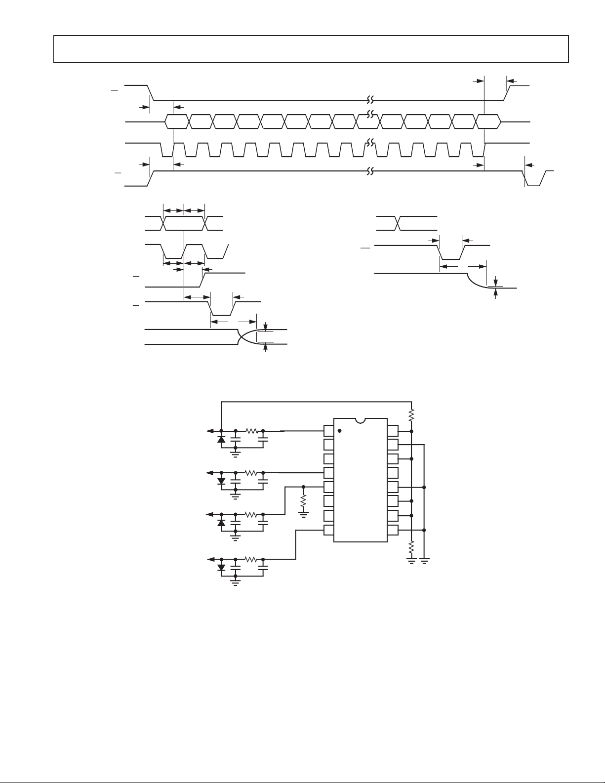
DAC8420
DATA LOAD SEQUENCE
CS
SDI
CLK
LD
DATA LOAD TIMING
t
CSH
t
S
CS
A1 A0 X X D11 D10 D9 D8 D4 D3 D2 D1 D0
t
LD1
t
t
DH
DS
SDI
CLK
t
CL
CS
LD
V
OUT
t
CH
t
CSH
t
LD2
t
LDW
t
S
±1LSB
CLEAR TIMING
CLSEL
CLR
V
OUT
t
CLRW
t
S
t
LD2
±1LSB
+15V
1N4001
–10V
1N4001
+10V
1N4001
–15V
1N4001
Figure 1. Timing Diagram
10kΩ
+
10µF 0.1µF
10kΩ
10µF 0.1µF
+
10kΩ
+
10µF 0.1µF
NC
NC
5kΩ
NC
10kΩ
10µF 0.1µF
+
Figure 2. Burn-In Diagram
1
2
3
4
5
6
NC
7
8
NC = NO CONNECT
DUT
16
15
14
13
12
11
10
9
5kΩ
NC
10kΩ
REV. A
–5–
DAC8420
PDIP and CERDIP
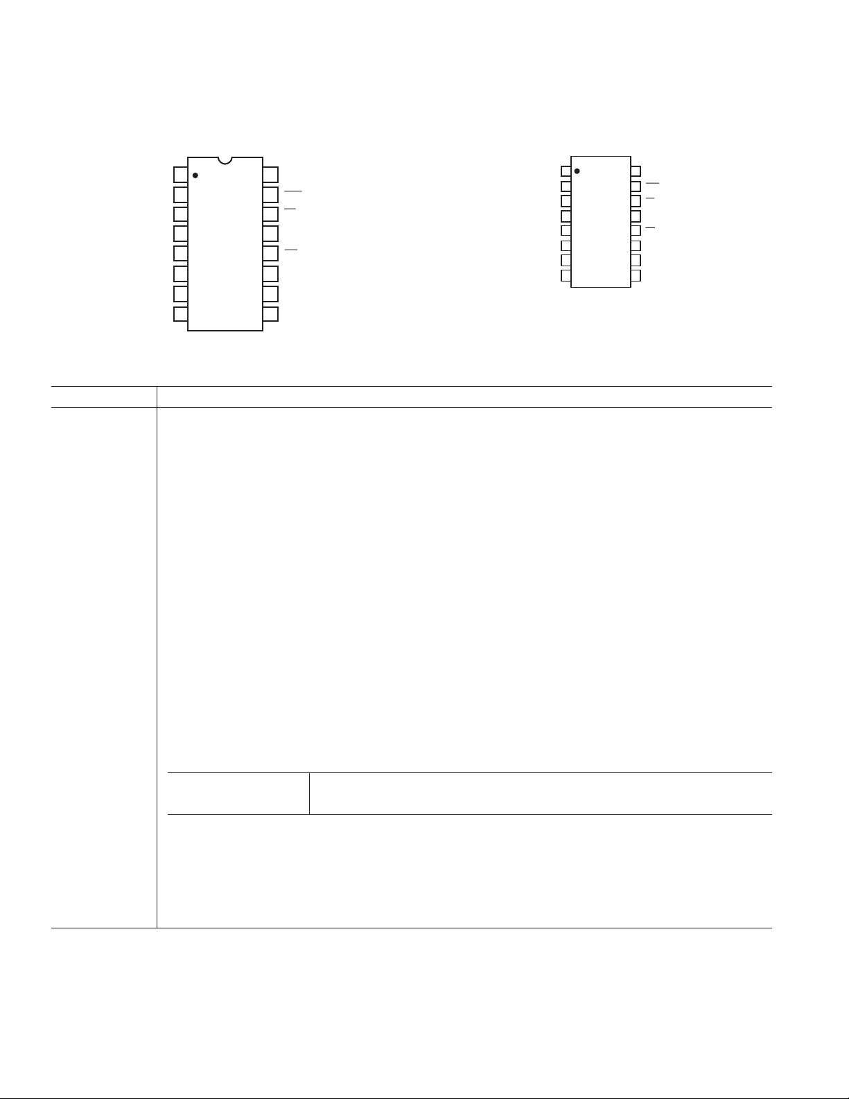
PIN CONFIGURATIONS
SOIC
VDD
VOUTD
VOUTC
VREFLO
VREFHI
VOUTB
VOUTA
VSS
1
2
3
4
DAC8420
TOP VIEW
5
(Not to Scale)
6
7
8
NC = NO CONNECT
1
CLSEL
16
15
CLR
LD
14
13
NC
CS
12
CLK
11
SDI
10
9
GND
VDD
VOUTD
VOUTC
VREFLO
VREFHI
VOUTB
VOUTA
VSS
2
DAC-8420
TOP VIEW
3
DAC-8420
(Not to Scale)
DAC8420
4
TOP VIEW
TOP VIEW
5
(Not to Scale)
(Not to Scale)
6
7
8
NC = NO CONNECT
16
CLSEL
15
CLR
14
LD
13
NC
12
CS
11
CLK
10
SDI
9
GND
PIN FUNCTION DESCRIPTIONS
Mnemonic Description
Power Supplies VDD: Positive Supply, 5 V to 15 V.
VSS: Negative Supply, 0 V to –15 V.
GND: Digital Ground.
Clock CLK: System Serial Data Clock Input, TTL/CMOS Levels. Data presented to the input SDI is shifted into
the internal serial-parallel input register on the rising edge of clock. This input is logically ORed with CS.
Control Inputs (All are CMOS/TTL compatible.)
CLR: Asynchronous Clear, Active Low. Sets internal data registers A through D to zero or midscale, depending on current state of CLSEL. The data in the serial input shift register is unaffected by this control.
CLSEL: Determines action of CLR. If High, a clear command will set the internal DAC registers A through D
to midscale (0x800). If low, the registers are set to zero (0x000).
CS: Device Chip Select, Active low. This input is logically ORed with the clock and disables the serial data
register input when high. When low, data input clocking is enabled. See Table I.
LD: Asynchronous DAC Register Load Control, Active Low. The data currently contained in the serial input
shift register is shifted out to the DAC data registers on the falling edge of LD, independent of CS. Input data
must remain stable while LD is low.
Data Input (All are CMOS/TTL compatible.)
SDI: Serial Data Input. Data presented to this pin is loaded into the internal serial-parallel shift register, which
shifts data in beginning with DAC address Bit A1. This input is ignored when CS is high.
The format of the 16-bit serial word is
(FIRST) (LAST)
B0 B1 B2 B3 B4 B5 B6 B7 B8 B9 B10 B11 B12 B13 B14 B15
A1 A0 NC NC D11 D10 D9 D8 D7 D6 D5 D4 D3 D2 D1 D0
—Address Word— (MSB) —DAC Data-Word— (LSB)
NC = Don’t Care.
Reference Inputs VREFHI: Upper DAC ladder reference voltage input. Allowable range is (VDD – 2.5 V) to (V
VREFLO: Lower DAC ladder reference voltage input, equal to zero-scale output. Allowable range is V
(V
VREFHI
– 2.5 V).
VREFLO
+ 2.5 V).
to
SS
Analog Outputs VOUTA through VOUTD: Four buffered DAC voltage outputs.
–6– REV. A
 Loading...