Analog Devices DAC8420 Datasheet

Quad 12-Bit Serial
a
FEATURES
Guaranteed Monotonic Over Temperature
Excellent Matching Between DACs
Unipolar or Bipolar Operation
Buffered Voltage Outputs
High Speed Serial Digital Interface
Reset to Zero- or Center-Scale
Wide Supply Range, +5 V-Only to 615 V
Low Power Consumption (35 mW max)
Available in 16-Pin DIP and SOL Packages
APPLICATIONS
Software Controlled Calibration
Servo Controls
Process Control and Automation
ATE
GENERAL DESCRIPTION
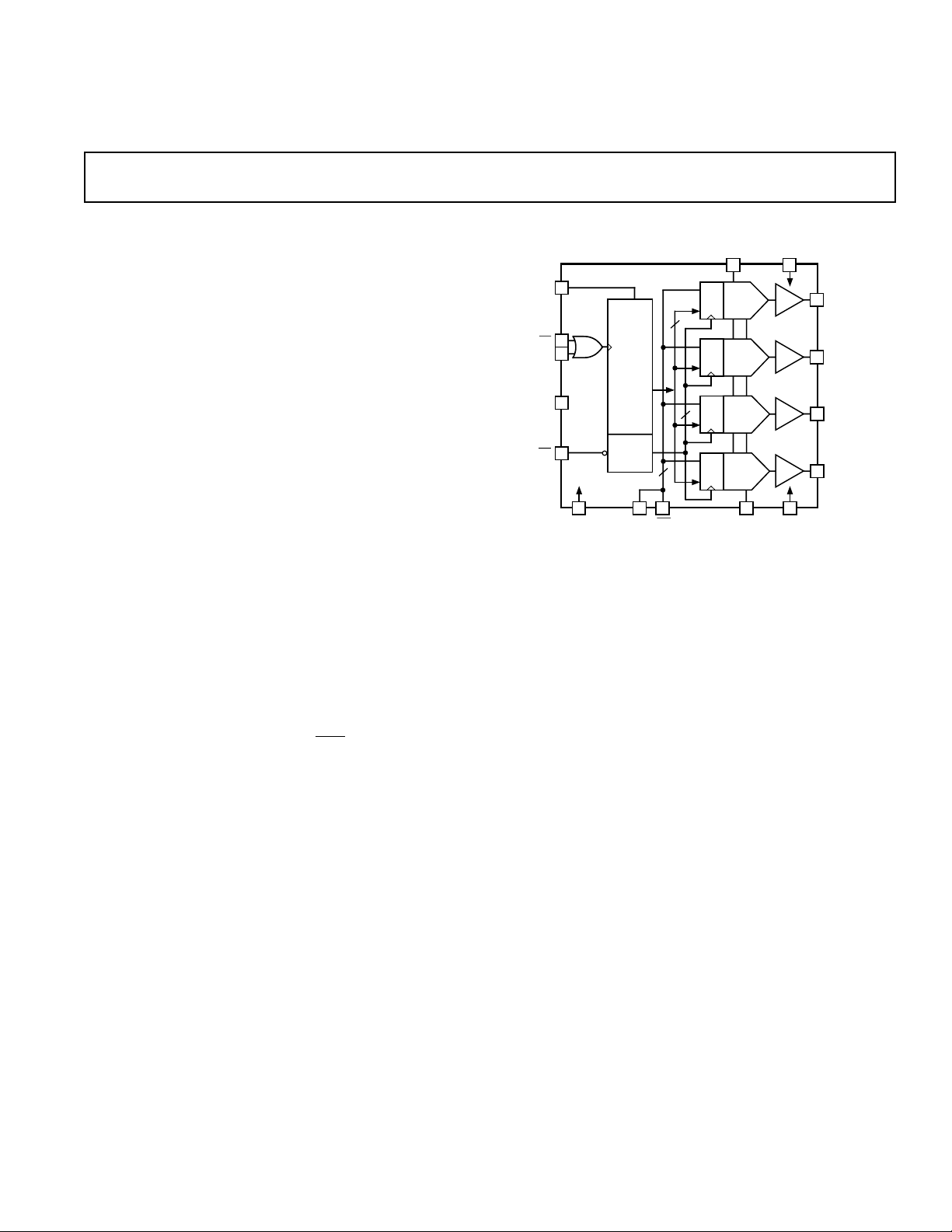
The DAC8420 is a quad, 12-bit voltage-output DAC with serial
digital interface, in a 16-pin package. Utilizing BiCMOS technology, this monolithic device features unusually high circuit
density and low power consumption. The simple, easy-to-use
serial digital input and fully buffered analog voltage outputs
require no external components to achieve specified performance.
The three-wire serial digital input is easily interfaced to microprocessors running at 10 MHz rates, with minimal additional
circuitry. Each DAC is addressed individually by a 16-bit serial
word consisting of a 12-bit data word and an address header.
The user-programmable reset control
outputs to either zero or midscale, asynchronously overriding
the current DAC register values. The output voltage range, determined by the inputs VREFHI and VREFLO, is set by the
user for positive or negative unipolar or bipolar signal swings
within the supplies allowing considerable design flexibility.
CLR forces all four DAC
Voltage Output DAC
DAC8420
FUNCTIONAL BLOCK DIAGRAM
VREFHI
5
10
SDI
CLK
12
CS
11
NC
13
14
LD
GND
SHIFT
REGISTER
DECODE
CLSEL
CLR
REG
REG
DAC A
A
A
12
REG
DAC B
B
REG
DAC C
4
C
REG
DAC D
D
2
VREFLO VSS
The DAC8420 is available in 16-pin epoxy DIP, cerdip, and
wide-body SOL (small-outline surface mount) packages. Operation is specified with supplies ranging from +5 V-only to ± 15 V,
with references of +2.5 V to ±10 V respectively. Power dissipation when operating from ±15 V supplies is less than 255 mW
(max), and only 35 mW (max) with a +5 V supply.
For applications requiring product meeting MIL-STD-883,
contact your local sales office for the DAC8420/883 data sheet,
which specifies operation over the –55°C to +125°C temperature range.
VDD
1
VOUTA
7
VOUTB
6
3
VOUTC
2
VOUTD
815169
4
REV. 0
Information furnished by Analog Devices is believed to be accurate and
reliable. However, no responsibility is assumed by Analog Devices for its
use, nor for any infringements of patents or other rights of third parties
which may result from its use. No license is granted by implication or
otherwise under any patent or patent rights of Analog Devices.
One Technology Way, P.O. Box 9106, Norwood, MA 02062-9106, U.S.A.
Tel: 617/329-4700 Fax: 617/326-8703

DAC8420–SPECIFICATIONS
ELECTRICAL CHARACTERISTICS
VSS = –5.0 V 6 5%, V
= –2.5 V, –408C ≤ TA ≤ +858C unless otherwise noted. See Note 1 for supply variations.)
VREFLO
(at VDD = +5.0 V 6 5%, VSS = 0.0 V, V
VREFHI
= +2.5 V, V
= 0.0 V, and
VREFLD
Parameter Symbol Condition Min Typ Max Units
STATIC ACCURACY
Integral Linearity “E” INL ±1/4 ±1 LSB
Integral Linearity “E” INL Note 2, V
= 0 V ±1/2 ±3 LSB
SS
Integral Linearity “F” INL ±3/4 ±2 LSB
Integral Linearity “F” INL Note 2, V
= 0 V ±1 ±4 LSB
SS
Differential Linearity DNL Monotonic Over Temperature ±1/4 ±1 LSB
Min-Scale Error ZSE R
Full-Scale Error FSE R
Min-Scale Error ZSE Note 2, R
Full-Scale Error FSE Note 2, R
Min-Scale Tempco TC
Full-Scale Tempco TC
ZSE
FSE
= 2 kΩ, VSS = –5 V ±4 LSB
L
= 2 kΩ, VSS = –5 V ±4 LSB
L
= 2 kΩ, VSS = 0 V ±8 LSB
L
= 2 kΩ, VSS = 0 V ±8 LSB
L
Note 3, RL = 2 kΩ, VSS = –5 V ±10 ppm/°C
Note 3, RL = 2 kΩ, VSS = –5 V ±10 ppm/°C
MATCHING PERFORMANCE
Linearity Matching ±1 LSB
REFERENCE
Positive Reference Input Range V
Negative Reference Input Range V
Negative Reference Input Range V
Reference High Input Current I
Reference Low Input Current I
VREFHI
VREFLO
VREFLO
VREFHI
VREFLO
Note 4 V
Note 4 V
Note 4, VSS = 0 V 0 V
Codes 000H, 555
H
–0.75 ±0.25 +0.75 mA
Codes 000H, 555H, VSS = –5 V –1.0 –0.6 mA
+2.5 VDD –2.5 V
VREFLO
SS
V
VREFHI
VREFHI
–2.5 V
–2.5 V
AMPLIFIER CHARACTERISTICS
Output Current I
Settling Time t
OUT
S
VSS = –5 V –1.25 +1.25 mA
to 0.01%, Note 5 8 µs
Slew Rate SR 10% to 90%, Note 5 1.5 V/µs
LOGIC CHARACTERISTICS
Logic Input High Voltage V
Logic Input Low Voltage V
Logic Input Current I
Input Capacitance C
LOGIC TIMING CHARACTERISTICS
Data Setup Time t
Data Hold t
Clock Pulse Width HIGH t
Clock Pulse Width LOW t
Select Time t
Deselect Delay t
Load Disable Time t
Load Delay t
Load Pulse Width t
Clear Pulse Width t
3, 6
INH
INL
IN
IN
DS
DH
CH
CL
CSS
CSH
LD1
LD2
LDW
CLRW
Note 3 13 pF
2.4 V
0.8 V
10 µA
25 ns
55 ns
90 ns
120 ns
90 ns
5ns
130 ns
35 ns
80 ns
150 ns
SUPPLY CHARACTERISTICS
Power Supply Sensitivity PSRR 0.002 0.01 %/%
Positive Supply Current I
Negative Supply Current I
Power Dissipation P
NOTES
1
All supplies can be varied ±5% and operation is guaranteed. Device is tested with VDD = +4.75 V.
2
For single-supply operation (V
3
Guaranteed but not tested.
4
Operation is guaranteed over this reference range, but linearity is neither tested nor guaranteed.
5
V
swing between +2.5 V and –2.5 V with VDD = 5.0 V.
OUT
6
All input control signals are specified with tr = tf =5 ns (10% to 90% of +5 V) and timed from a voltage level of 1.6 V.
7
Typical values indicate performance measured at +25°C.
Specifications subject to change without notice.
= 0 V, VSS = 0 V), due to internal offset errors INL and DNL are measured beginning at code 003H.
VREFLO
DD
SS
DISS
–6 –3 mA
VSS = 0 V 20 35 mW
47 mA
–2–
REV. 0

DAC8420
ELECTRICAL CHARACTERISTICS
V
= –10.0 V, –408C ≤ TA ≤ +858C unless otherwise noted. See Note 1 for supply variations.)
VREFLO
(at VDD = +15.0 V 6 5%, VSS = –15.0 V 6 5%, V
VREFHI
= +10.0 V,
Parameter Symbol Condition Min Typ Max Units
STATIC ACCURACY
Integral Linearity “E” INL ±1/4 ±1/2 LSB
Integral Linearity “F” INL ±1/2 ±1 LSB
Differential Linearity DNL Monotonic Over Temperature ± 1/4 ±1 LSB
Min-Scale Error ZSE R
Full-Scale Error FSE R
Min-Scale Tempco TC
Full-Scale Tempco TC
ZSE
FSE
= 2 kΩ±2 LSB
L
= 2 kΩ±2 LSB
L
Note 2, RL = 2 kΩ±4 ppm/°C
Note 2, RL = 2 kΩ±4 ppm/°C
MATCHING PERFORMANCE
Linearity Matching ±1 LSB
REFERENCE
Positive Reference Input Range V
Negative Reference Input Range V
Reference High Input Current I
Reference Low Input Current I
VREFHI
VREFLO
VREFHI
VREFLO
Note 3 V
Note 3 –10 V
Codes 000H, 555
Codes 000H, 555
H
H
+2.5 VDD –2.5 V
VREFLO
VREFHI
–2.5 V
–2.0 ±1.0 +2.0 mA
–3.5 –2.0 mA
AMPLIFIER CHARACTERISTICS
Output Current I
Settling Time t
OUT
S
to 0.01%, Note 4 13 µs
–5 +5 mA
Slew Rate SR 10% to 90%, Note 4 2 V/µs
DYNAMIC PERFORMANCE
Analog Crosstalk Note 2 >64 dB
Digital Feedthrough Note 2 >72 dB
Large Signal Bandwidth 3 dB, V
V
VREFLO
= 5 V + 10 V p-p, 90 kHz
VREFHI
= –10 V, Note 2
Glitch Impulse Code Transition = 7FFH to 800H, Note 2 64 nV-s
LOGIC CHARACTERISTICS
Logic Input High Voltage V
Logic Input Low Voltage V
Logic Input Current I
Input Capacitance C
LOGIC TIMING CHARACTERISTICS
2, 5
Data Setup Time t
Data Hold t
Clock Pulse Width HIGH t
Clock Pulse Width LOW t
Select Time t
Deselect Delay t
Load Disable Time t
Load Delay t
Load Pulse Width t
Clear Pulse Width t
INH
INL
IN
IN
DS
DH
CH
CL
CSS
CSH
LD1
LD2
LDW
CLRW
Note 2 13 pF
2.4 V
0.8 V
10 µA
25 ns
20 ns
30 ns
50 ns
55 ns
15 ns
40 ns
15 ns
45 ns
70 ns
SUPPLY CHARACTERISTICS
Power Supply Sensitivity PSRR 0.002 0.01 %/%
Positive Supply Current I
Negative Supply Current I
Power Dissipation P
NOTES
1
All supplies can be varied ±5% and operation is guaranteed.
2
Guaranteed but not tested.
3
Operation is guaranteed over this reference range, but linearity is neither tested nor guaranteed.
4
V
swing between +10 V and –10 V.
OUT
5
All input control signals are specified with tr = tf =5 ns (10% to 90% of +5 V) and timed from a voltage level of 1.6 V.
6
Typical values indicate performance measured at +25°C.
Specifications subject to change without notice.
DD
SS
DISS
–8 –5 mA
69 mA
255 mW
REV. 0
–3–

DAC8420
10
SDI
9
GND
8
VSS
7
VOUTA
CLR
15
CLSEL
16
(SUBSTRATE)
VDD
1
VOUTD
2
VOUTC 3
VREFLO 4
VREFHI 5
VOUTB 6
11 CLK
12 CS
14 LD
13 NC
NC = NO CONNECT
WAFER TEST LIMITS
(at VDD = +15.0 V, VSS = –15.0 V, V
unless otherwise noted)
= +10.0 V, V
REFHI
= –10.0 V, TA = +258C
REFLO
DAC8420G
Parameter Symbol Conditions Limit Units
Integral Linearity INL ±1 LSB max
Differential Linearity DNL ±1 LSB max
Min-Scale Offset ±1 LSB max
Max-Scale Offset ±1 LSB max
Logic Input High Voltage V
Logic Input Low Voltage V
Logic Input Current I
Positive Supply Current I
Negative Supply Current I
NOTE
Electrical tests are performed at wafer probe to the limits shown. Due to variations in assembly methods and normal yield loss, yield after packaging is not guaranteed
for standard product dice. Consult factory to negotiate specifications based on dice lot qualification through sample lot assembly and testing.
ABSOLUTE MAXIMUM RATINGS
(TA = +25°C unless otherwise noted)
VDD to GND . . . . . . . . . . . . . . . . . . . . . . . . . –0.3 V, +18.0 V
V
to GND . . . . . . . . . . . . . . . . . . . . . . . . . . +0.3 V, –18.0 V
SS
V
to VDD . . . . . . . . . . . . . . . . . . . . . . . . . . . –0.3 V, +36.0 V
SS
V
to V
SS
V
VREFHI
V
VREFHI
I
VREFHI
to V
to VDD . . . . . . . . . . . . . . . . . . . . . . . +2.0 V, +33.0 V
, I
. . . . . . . . . . . . . . . . . . . . . . –0.3 V, VSS – 2.0 V
VREFLO
VREFLO
. . . . . . . . . . . . . . . . . . . +2.0 V, VDD – V
VREFLO
. . . . . . . . . . . . . . . . . . . . . . . . . . . . . . . 10 mA
Digital Input Voltage to GND . . . . . . . . . –0.3 V, V
IN
DD
SS
INH
INL
+ 0.3 V
DD
3. Remove power before inserting or removing units from their
sockets.
4. Analog Outputs are protected from short circuits to ground
or either supply.
SS
DICE CHARACTERISTICS
2.4 V min
0.8 V max
1 µA max
8 mA max
7 mA max
Output Short Circuit Duration . . . . . . . . . . . . . . . . Indefinite
Operating Temperature Range
EP, FP, ES, FS, EQ, FQ . . . . . . . . . . . . . . –40°C to +85°C
Dice Junction Temperature . . . . . . . . . . . . . . . . . . . . . +150°C
Storage Temperature . . . . . . . . . . . . . . . . . . –65°C to +150°C
Power Dissipation . . . . . . . . . . . . . . . . . . . . . . . . . . 1000 mW
Lead Temperature (Soldering, 60 sec) . . . . . . . . . . . . . +300°C
Package Type θ
16-Pin Plastic DIP (P) 70
16-Pin Hermetic DIP (Q) 82
16-Lead Small Outline
Surface Mount (S) 86
NOTES
1
θJA is specified for worst case mounting conditions, i.e., θJA is specified for
device in socket.
2
θJA is specified for device on board.
Thermal Resistance
JA
1
1
2
θ
JC
Units
27 °C/W
9 °C/W
22 °C/W
CAUTION
1. Stresses above those listed under “Absolute Maximum Rat-
ings” may cause permanent damage to the device. This is a
stress rating only and functional operation at or above this
specification is not implied. Exposure to the above maximum
rating conditions for extended periods may affect device
reliability.
2. Digital inputs and outputs are protected, however, permanent
damage may occur on unprotected units from high-energy
electrostatic fields. Keep units in conductive foam or packaging
at all times until ready to use. Use proper antistatic handling
procedures.
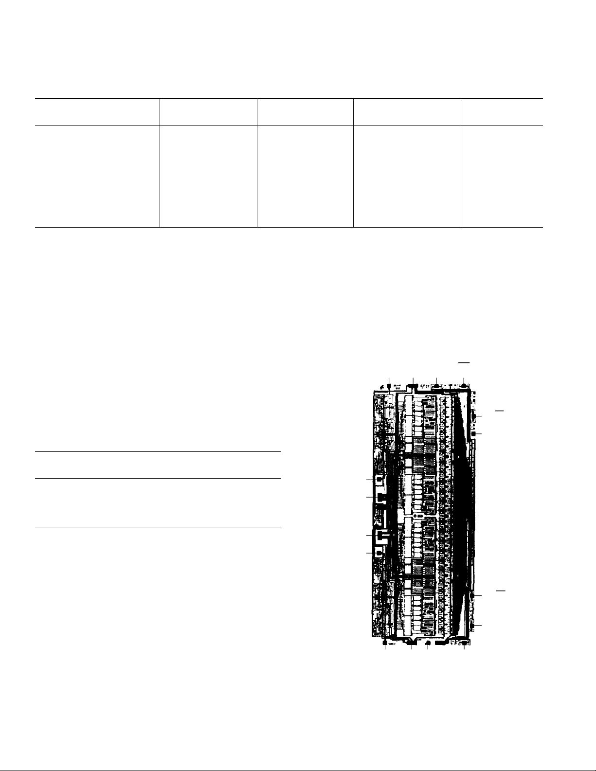
Die Size 0.119 × 0.283 inch, 33,677 sq. mils
×
(3.023
7.188 mm, 21.73 sq. mm)
Transistor Count 2,207
For additional DICE ordering information, refer to databook.
–4–
REV. 0

DAC8420
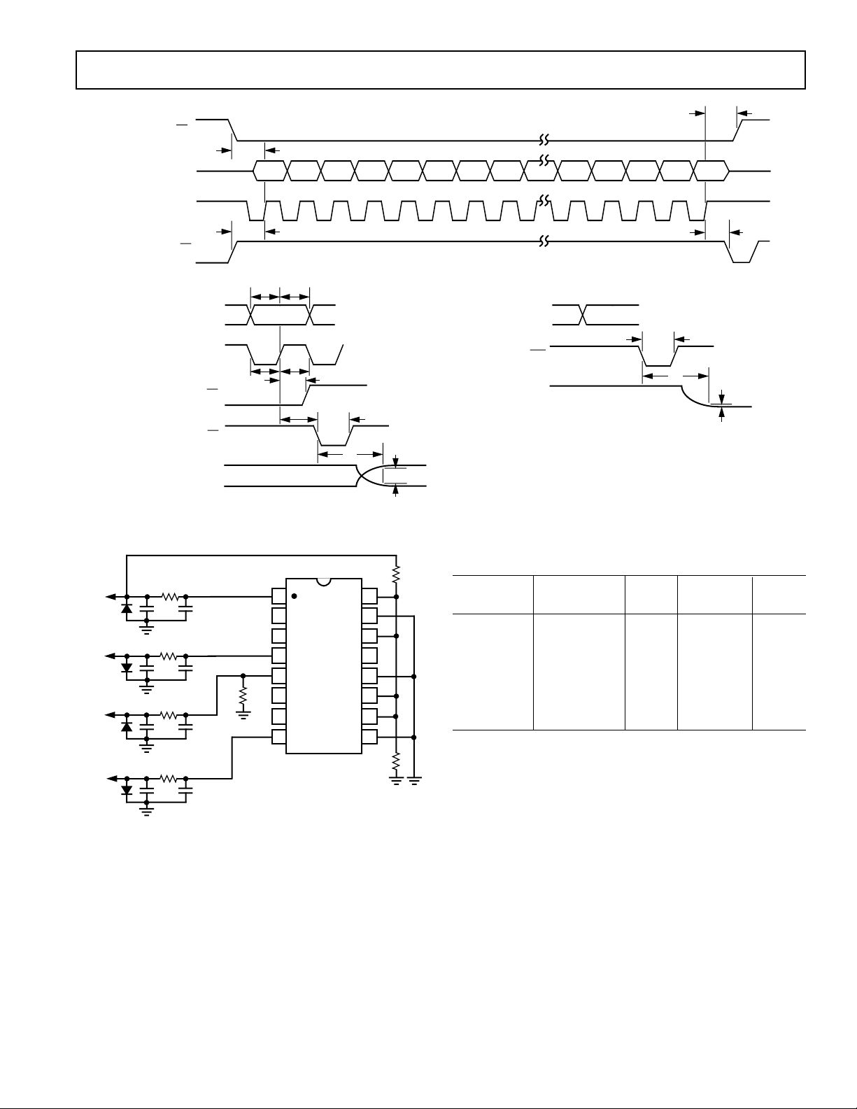
DATA LOAD SEQUENCE
CS
SDI
CLK
LD
DATA LOAD TIMING
SDI
CLK
CS
LD
V
OUT
t
CSS
A1 A0 X X D11 D10 D9 D8 D4 D3 D2 D1 D0
t
LD1
t
t
DH
DS
CLEAR TIMING
CLSEL
t
t
t
CL
CH
t
CSH
t
LD2
t
LDW
t
S
±1LSB
CLR
V
OUT
Timing Diagram
CLRW
t
CSH
t
LD2
t
S
±1LSB
+15V
1N4001
–10V
1N4001
+10V
1N4001
–15V
1N4001
10Ω
+
10µF 0.1µF
10Ω
10µF 0.1µF
+
10Ω
+
10µF 0.1µF
10Ω
10µF 0.1µF
+
1
2
NC
NC
3
4
5
5kΩ
6
NC
NC
7
8
NC = NO CONNECT
Burn-In Diagram
DUT
16
15
14
13
12
11
10
9
5kΩ
10kΩ
NC
ORDERING GUIDE
1
Model
DAC8420EP –40°C to +85°C 0.5 Plastic DIP P
DAC8420EQ –40°C to +85°C 0.5 Cerdip Q
DAC8420ES –40°C to +85°C 0.5 SOIC SOL
DAC8420FP –40°C to +85°C 1.0 Plastic DIP P
DAC8420FQ –40°C to +85°C 1.0 Cerdip Q
DAC8420FS –40°C to +85°C 1.0 SOIC SOL
DAC8420QBC –40°C to +85°C 1.0 Dice
NOTES
1
A complete /883 data sheet is available. For availability and burn-in information, contact your local sales office.
2
PMI division letter designator.
3
Dice tested at +25°C only.
Temperature INL Package Package
Range (6LSB) Description Option
3
2
REV. 0
–5–
 Loading...