

Quad, 12-Bit DAC
a
FEATURES
+5 V to ⴞ15 V Operation
Unipolar or Bipolar Operation
True Voltage Output
Double-Buffered Inputs
Reset to Min (DAC8413) or Center Scale (DAC8412)
Fast Bus Access Time
Readback
APPLICATIONS
Automatic Test Equipment
Digitally Controlled Calibration
Servo Controls
Process Control Equipment
GENERAL DESCRIPTION
The DAC8412 and DAC8413 are quad, 12-bit voltage output
DACs with readback capability. Built using a complementary
BiCMOS process, these monolithic DACs offer the user very
high package density.
Output voltage swing is set by the two reference inputs V
and V
. By setting the V
REFL
input to 0 V and V
REFL
positive voltage, the DAC will provide a unipolar positive output
range. A similar configuration with V
at 0 V and V
REFH
a negative voltage will provide a unipolar negative output range.
Bipolar outputs are configured by connecting both V
to nonzero voltages. This method of setting output voltage
V
REFL
range has advantages over other bipolar offsetting methods because
it is not dependent on internal and external resistors with different
temperature coefficients.
REFH
REFH
to a
REFL
and
REFH
at
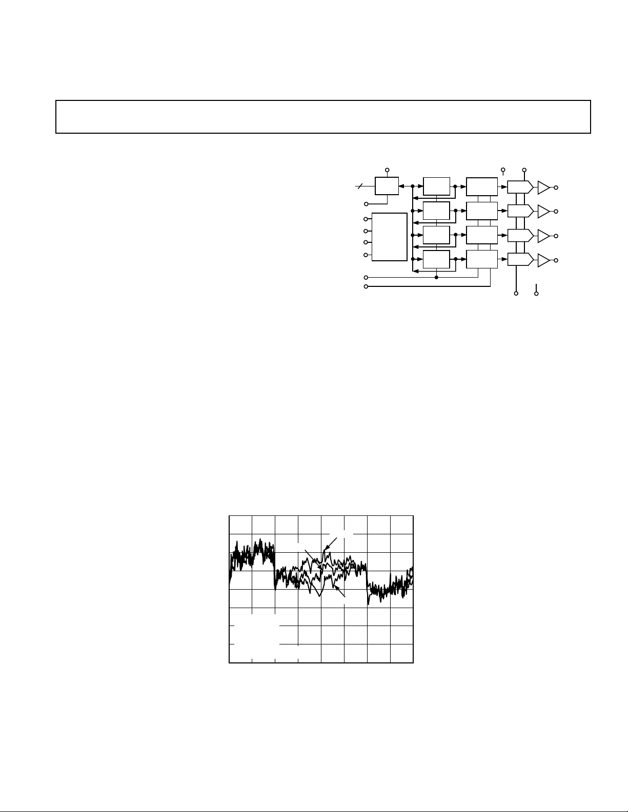
Voltage Output with Readback
DAC8412/DAC8413
FUNCTIONAL BLOCK DIAGRAM
V
LOGIC
12
CS
A0
A1
I/O
PORT
CONTROL
LOGIC
INPUT
REG
INPUT
REG B
INPUT
REG C
INPUT
REG D
OUTPUT
A
REG
OUTPUT
REG B
OUTPUT
REG C
OUTPUT
REG D
DATA
I/O
DGND
RESET
LDAC
R/W
Digital controls allow the user to load or read back data from any
DAC, load any DAC and transfer data to all DACs at one time.
An active low RESET loads all DAC output registers to midscale for the DAC8412 and zero scale for the DAC8413.
The DAC8412/DAC8413 are available in 28-lead plastic DIP,
PLCC and LCC packages. They can be operated from a wide
variety of supply and reference voltages with supplies ranging
from single +5 V to ±15 V, and references from +2.5 V to ±10 V.
Power dissipation is less than 330 mW with ±15 V supplies and
only 60 mW with a +5 V supply.
For MIL-STD-883 applications, contact your local ADI sales
office for the DAC8412/DAC8413/883 data sheet which specifies
operation over the –55°C to +125°C temperature range. All
883 parts are also available on Standard Military Drawings
5962-91 76401MXA through 76404M3A.
V
V
REFH
DD
A
DAC
A
DAC B
DAC C
DAC
D
V
REFLVSS
V
V
V
V
OUTA
OUTB
OUTC
OUTD
0.500
0.375
0.250
0.125
0
–0.125
–0.250
–0.375
–0.500
VDD = +15V
V
= –15V
SS
V
= +10V
REFH
V
= –10V
REFL
T
= –55ⴗC, +25ⴗC, +125ⴗC
A
0 4096512
LINEARITY ERROR – LSB
+25ⴗC
1024 1536 2046 2548 2560 3072
DIGITAL INPUT CODE – Decimal
Figure 1. INL vs. Code Over Temperature
REV. D
Information furnished by Analog Devices is believed to be accurate and
reliable. However, no responsibility is assumed by Analog Devices for its
use, nor for any infringements of patents or other rights of third parties
which may result from its use. No license is granted by implication or
otherwise under any patent or patent rights of Analog Devices.
+125ⴗC
–55ⴗC
One Technology Way, P.O. Box 9106, Norwood, MA 02062-9106, U.S.A.
Tel: 781/329-4700 World Wide Web Site: http://www.analog.com
Fax: 781/326-8703 © Analog Devices, Inc., 2000

DAC8412/DAC8413–SPECIFICATIONS
(@ V
= +15.0 V, VSS = –15.0 V, V
DD
ELECTRICAL CHARACTERISTICS
–40ⴗC ≤ TA ≤ +85ⴗC unless otherwise noted. See Note 1 for supply variations.)
Parameter Symbol Conditions Min Typ Max Units
Integral Nonlinearity Error INL E Grade 0.25 ±0.5 LSB
INL F Grade ± 1 LSB
Differential Nonlinearity Error DNL Monotonic Over Temperature –1 LSB
Min-Scale Error V
Full-Scale Error V
ZSE
FSE
Min-Scale Tempco TCV
Full-Scale Tempco TCV
RL = 2 kΩ±2 LSB
RL = 2 kΩ±2 LSB
RL = 2 kΩ 15 ppm/°C
ZSE
RL = 2 kΩ 20 ppm/°C
FSE
Linearity Matching Adjacent DAC Matching ± 1 LSB
REFERENCE
Positive Reference Input Voltage Range Note 2 V
Negative Reference Input Voltage Range Note 2 –10 V
Reference High Input Current I
Reference Low Input Current I
Large Signal Bandwidth BW –3 dB, V
REFH
REFL
= 0 V to +10 V p-p 160 kHz
REFH
AMPLIFIER CHARACTERISTICS
Output Current I
Settling Time t
OUT
S
RL = 2 kΩ, CL = 100 pF –5 +5 mA
to 0.01%, 10 V Step, RL = 1 kΩ 10 µs
Slew Rate SR 10% to 90% 2.2 V/µs
Analog Crosstalk 72 dB
LOGIC CHARACTERISTICS
Logic Input High Voltage V
Logic Input Low Voltage V
Logic Output High Voltage V
Logic Output Low Voltage V
Logic Input Current I
Input Capacitance C
Digital Feedthrough
LOGIC TIMING CHARACTERISTICS
3
3
Chip Select Write Pulsewidth t
Write Setup t
Write Hold t
Address Setup t
Address Hold t
Load Setup t
Load Hold t
Write Data Setup t
Write Data Hold t
Load Data Pulsewidth t
Reset Pulsewidth t
Chip Select Read Pulsewidth t
Read Data Hold t
Read Data Setup t
Data to Hi Z t
Chip Select to Data t
INH
INL
OH
OL
IN
IN
WCS
WS
WH
AS
AH
LS
LH
WDS
WDH
LDW
RESET
RCS
RDH
RDS
DZ
CSD
TA = +25°C2.4 V
TA = +25°C 0.8 V
IOH = +0.4 mA 2.4 V
IOL = –1.6 mA 0.4 V
V
= +2.5 V, V
REFH
REFL
Note 4
t
= 80 ns 0 ns
WCS
t
= 80 ns 0 ns
WCS
t
= 80 ns 20 ns
WCS
t
= 80 ns 0 ns
WCS
t
= 130 ns 0 ns
RCS
t
= 130 ns 0 ns
RCS
CL = 10 pF 200 ns
CL = 100 pF 160 ns
SUPPLY CHARACTERISTICS
Power Supply Sensitivity PSS 14.25 V ≤ V
Positive Supply Current I
Negative Supply Current I
Power Dissipation P
NOTES
1
All supplies can be varied ± 5%, and operation is guaranteed. Device is tested with nominal supplies.
2
Operation is guaranteed over this reference range, but linearity is neither tested nor guaranteed.
3
All parameters are guaranteed by design.
4
All input control signals are specified with tr = tf = 5 ns (10% to 90% of +5 V) and timed from a voltage level of 1.6 V.
Specifications subject to change without notice.
DD
SS
DISS
V
= +2.5 V 8.5 12 mA
REFH
≤ 15.75 V 150 ppm/V
DD
= +5.0 V, V
LOGIC
= +10.0 V, V
REFH
+ 2.5 VDD – 2.5 V
REFL
= –10.0 V,
REFL
REFH
– 2.5 V
–2.75 +1.5 +2.75 mA
0 +2 +2.75 mA
1 µA
8pF
= 0 V 5 nV-s
80 ns
0ns
0ns
70 ns
30 ns
170 ns
140 ns
130 ns
–10 –6.5 mA
330 mW
–2–
REV. D

DAC8412/DAC8413
(@ V
= V
= +5.0 V ⴞ 5%, VSS = 0.0 V, V
LOGIC
ELECTRICAL CHARACTERISTICS
DD
V
= –2.5 V, –40ⴗC ≤ TA ≤ +85ⴗC unless otherwise noted. See Note 1 for supply variations.)
REFL
Parameter Symbol Conditions Min Typ Max Units
Integral Nonlinearity Error INL E Grade 1/2 ± 1 LSB
INL F Grade ± 2 LSB
INL V
INL V
= 0.0 V; E Grade
SS
= 0.0 V; F Grade
SS
2
2
Differential Nonlinearity Error DNL Monotonic Over Temperature –1 LSB
Min-Scale Error V
Full-Scale Error V
Min-Scale Error V
Full-Scale Error V
ZSE
FSE
ZSE
FSE
Min-Scale Tempco TCV
Full-Scale Tempco TCV
VSS = –5.0 V ± 4 LSB
VSS = –5.0 V ± 4 LSB
VSS = 0.0 V ± 8 LSB
VSS = 0.0 V ± 8 LSB
ZSE
FSE
Linearity Matching Adjacent DAC Matching ±1 LSB
REFERENCE
Positive Reference Input Voltage Range Note 3 V
Negative Reference Input Voltage Range V
Reference High Input Current I
REFH
Large Signal Bandwidth BW –3 dB, V
= 0.0 V 0 V
SS
= –5.0 V –2.5 V
V
SS
Code 000H –1.0 +1.0 mA
= 0 V to 2.5 V p-p 450 kHz
REFH
AMPLIFIER CHARACTERISTICS
Output Current I
Settling Time t
OUT
S
RL = 2 kΩ, CL = 100 pF –1.25 +1.25 mA
to 0.01%, 2.5 V Step, RL = 1 kΩ 7 µs
Slew Rate SR 10% to 90% 2.2 V/µs
LOGIC CHARACTERISTICS
Logic Input High Voltage V
Logic Input Low Voltage V
Logic Output High Voltage V
Logic Output Low Voltage V
Logic Input Current I
Input Capacitance C
LOGIC TIMING CHARACTERISTICS
4
Chip Select Write Pulsewidth t
Write Setup t
Write Hold t
Address Setup t
Address Hold t
Load Setup t
Load Hold t
Write Data Setup t
Write Data Hold t
Load Data Pulsewidth t
Reset Pulsewidth t
Chip Select Read Pulsewidth t
Read Data Hold t
Read Data Setup t
Data to Hi Z t
Chip Select to Data t
INH
INL
OH
OL
IN
IN
WCS
WS
WH
AS
AH
LS
LH
WDS
WDH
LDW
RESET
RCS
RDH
RDS
DZ
CSD
TA = +25°C2.4 V
TA = +25°C0.8V
IOH = +0.4 mA 2.4 V
IOL = –1.6 mA 0.45 V
Note 5
t
= 150 ns 0 ns
WCS
t
= 150 ns 0 ns
WCS
t
= 150 ns 20 ns
WCS
t
= 150 ns 0 ns
WCS
t
= 170 ns 20 ns
RCS
t
= 170 ns 0 ns
RCS
CL = 10 pF 200 ns
CL = 100 pF 320 ns
SUPPLY CHARACTERISTICS
Power Supply Sensitivity PSS 100 ppm/V
Positive Supply Current I
Negative Supply Current I
Power Dissipation P
DD
SS
DISS
VSS = –5.0 V –10 mA
VSS = 0 V 60 mW
VSS = –5 V 110 mW
NOTES
1
All supplies can be varied ± 5%, and operation is guaranteed. Device is tested with VDD = +4.75 V.
2
For single supply operation only (V
3
Operation is guaranteed over this reference range, but linearity is neither tested nor guaranteed.
4
All parameters are guaranteed by design.
5
All input control signals are specified with tr = tf = 5 ns (10% to 90% of +5 V) and timed from a voltage level of 1.6 V.
Specifications subject to change without notice.
REV. D
= 0.0 V, VSS = 0.0 V): Due to internal offset errors, INL and DNL are measured beginning at code 2 (002H).
REFL
–3–
= +2.5 V, V
REFH
= 0.0 V, and VSS = –5.0 V ⴞ 5%,
REFL
± 2 LSB
± 4 LSB
100 ppm/°C
100 ppm/°C
+ 2.5 VDD – 2.5 V
REFL
REFH
REFH
– 2.5 V
– 2.5 V
1 µA
8pF
150 ns
0ns
0ns
70 ns
50 ns
180 ns
150 ns
170 ns
712 mA
DAC8412/DAC8413
t
CS
t
RDS
RCS
t
RDH
R/W
t
AS
t
AH
A0/A1
t
DATA
OUT
HI-Z HI -Z
t
CSD
DATA VALID
DZ
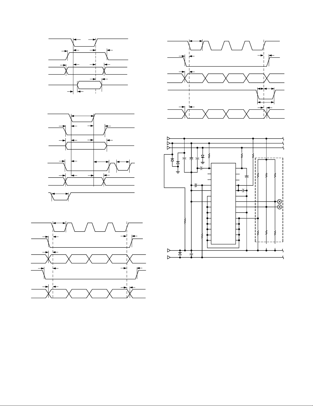
Figure 2. Data Output (Read Timing)
t
WCS
CS
t
WS
t
WH
R/W
t
AS
t
AH
A0/A1
t
t
LS
LH
t
LDW
LDAC
DATA
t
WDS
IN
t
RESET
t
WDH
RESET
Figure 3. Data WRITE (Input and Output Registers) Timing
80ns
CS
t
WH
t
LH
t
WDH
R/W
ADDRESS
LDAC
DATA
t
WS
t
AS
ADDRESS
ONE
IN
DATA1
VALID
t
t
LS
WDS
ADDRESS
TWO
DATA2
VALID
ADDRESS
THREE
DATA3
VALID
ADDRESS
FOUR
DATA4
VALID
CS
R/W
ADDRESS
LDAC
DATA IN
V
DD
V
REFH
V
REFL
DGND
V
SS
80ns
t
WS
t
AS
ADDRESS
ONE
DATA1
VALID
t
WDS
ADDRESS
TWO
DATA2
VALID
ADDRESS
THREE
DATA3
VALID
Figure 5. Double Buffer Mode
++
C1
C1
D1
C1
D1
C2
R6
D1
+
C1
V
= +15V, VSS = –15V, V
DD
R1
= 10⍀, R2 = 100⍀, R3 = 5k⍀, R4 = 10k⍀, R5 = 100k⍀,
R6 = 47⍀ FOR LCC, R6 = 100⍀ FOR DIP
C1 = 4.7F (ONCE PER PORT), C2 = 0.01F (EACH DEVICE)
D1 = 1N4001 OR EQUIVALENT (ONCE PER PORT)
R2
D1
+
C2
N/C
N/C
R1
V
V
V
V
V
DGND
RESET
LDAC
DB0
DB1
DB2
DB3
DB4
DB5
DB6 *
REFH
OUTB
OUTA
SS
REFH
REFL
V
OUTC
V
OUTD
V
DD
V
LOGIC
CS
A0
A1
R/W
DB11
DB10
DB9
DB8
DB7
= +10V, V
Figure 6. Burn-In Diagram
N/C
N/C
C2
REFL
ADDRESS
R2
C2
= 0V
FOUR
t
LS
DATA4
VALID
R1
R3
R5
ONCE PER PORT
t
LH
t
LDW
R3 R3
R4
t
t
WDH
WH
R4
Figure 4. Single Buffer Mode
–4–
REV. D
DAC8412/DAC8413
ABSOLUTE MAXIMUM RATINGS
(
TA = +25°C unless otherwise noted)
VSS to VDD . . . . . . . . . . . . . . . . . . . . . . . . . . . –0.3 V, +33.0 V
V
to V
SS
V
LOGIC
V
to V
SS
V
to VDD . . . . . . . . . . . . . . . . . . . . . . . . . +2.0 V, +33.0 V
REFH
to V
V
REFH
. . . . . . . . . . . . . . . . . . . . . . . . . –0.3 V, +33.0 V
LOGIC
to DGND . . . . . . . . . . . . . . . . . . . . . . –0.3 V, +7.0 V
. . . . . . . . . . . . . . . . . . . . . . . . –0.3 V, +VSS–2.0 V
REFL
. . . . . . . . . . . . . . . . . . . . . . . . +2.0 V, VSS–V
REFL
DD
Package Type JA* JCUnits
28-Lead Plastic DIP (P) 48 22 °C/W
28-Lead Hermetic Leadless Chip Carrier (TC) 70 28 °C/W
28-Lead Plastic Leaded Chip Carrier (PC) 63 25 °C/W
*θJA is specified for worst-case mounting conditions, i. e., θJA is specified for device
in socket.
Thermal Resistance
Current into Any Pin 4 . . . . . . . . . . . . . . . . . . . . . . . . ± 15 mA
Digital Input Voltage to DGND . . . . . –0.3 V, V
LOGIC
+0.3 V
Digital Output Voltage to DGND . . . . . . . . . . –0.3 V, +7.0 V
Operating Temperature Range
ET, FT, EP, FP, FPC . . . . . . . . . . . . . . . . –40°C to +85°C
AT, BT, BTC . . . . . . . . . . . . . . . . . . . . . –55°C to +125°C
Dice Junction Temperature . . . . . . . . . . . . . . . . . . . . . +150°C
Storage Temperature . . . . . . . . . . . . . . . . . . –65°C to +150°C
Power Dissipation Package . . . . . . . . . . . . . . . . . . . 1000 mW
Lead Temperature (Soldering, 60 sec) . . . . . . . . . . . . +300°C
ORDERING INFORMATION
1, 2
INL Military3 Temperature Extended Industrial3 Temperature Package Package
(LSB) –55ⴗC to +125ⴗC –40ⴗC to +85ⴗC Description Option
± 1 DAC8412FPC PLCC P-28A
± 1.5 DAC8412BTC/883 LCC E-28A
0.5 DAC8412EP Plastic DIP N-28
± 1 DAC8412FP Plastic DIP N-28
± 1 DAC8413FPC PLCC P-28A
± 1.5 DAC8413BTC/883 LCC E-28A
± 0.5 DAC8413EP Plastic DIP N-28
± 1 DAC8413FP Plastic DIP N-28
NOTES
1
Die Size 0.225 × 0.165 inches, 37,125 sq. mils (5.715 × 4.191 mm, 23.95 sq. mm). Substrate should be connected to VDD; Transistor Count = 2595.
2
Burn-in is available on extended industrial temperature range parts in cerdip.
3
A complete /883 data sheet is available. For availability and burn-in information, contact your local sales office.
CAUTION
1. Stresses above those listed under Absolute Maximum Ratings may cause permanent damage to the
device. This is a stress rating only; functional operation at or above this specification is not implied.
Exposure to the above maximum rating conditions for extended periods may affect
device reliability.
WARNING!
2. Digital inputs and outputs are protected, however, permanent damage may occur on unprotected units
from high-energy electrostatic fields. Keep units in conductive foam or packaging at all times until
ready to use. Use proper antistatic handling procedures.
3. Remove power before inserting or removing units from their sockets.
4. Analog outputs are protected from short circuit to ground or either supply.
REV. D
–5–
ESD SENSITIVE DEVICE

DAC8412/DAC8413
PIN FUNCTION DESCRIPTIONS
Pin Name Description
1V
2V
3V
4V
REFH
OUTB
OUTA
SS
High-Side DAC Reference Input
DAC B Output
DAC A Output
Lower-Rail Power Supply
5 DGND Digital Ground
6 RESET Reset Input and Output Registers to all 0s,
Enabled at Active Low
7 LDAC Load Data to DAC, Enabled at Active Low
8 DB0 Data Bit 0, LSB
9 DB1 Data Bit 1
10 DB2 Data Bit 2
11 DB3 Data Bit 3
12 DB4 Data Bit 4
13 DB5 Data Bit 5
14 DB6 Data Bit 6
15 DB7 Data Bit 7
16 DB8 Data Bit 8
17 DB9 Data Bit 9
18 DB10 Data Bit 10
19 DB11 Data Bit 11, MSB
20 R/W Active Low to Write Data to DAC. Active
High to Readback Previous Data at Data Bit
Pins with V
Connected to +5 V
LOGIC
21 A1 Address Bit 1
22 A0 Address Bit 0
23 CS Chip Select, Enabled at Active Low
24 V
LOGIC
Voltage Supply for Readback Function. Can
be Open Circuit If Not Used
25 V
26 V
27 V
28 V
DD
OUTD
OUTC
REFL
Upper-Rail Power Supply
DAC D Output
DAC C Output
Low-Side DAC Reference Input
DB0
DB0
DGND
RESET
LDAC
(LSB)
DB1
DB2
DB3
PIN CONFIGURATIONS
Plastic DIP
V
1
REFH
V
OUTB
2
V
3
OUTA
V
4
SS
DAC8412
5
DGND
RESET
LDAC
(LSB)
DB1
DB2
DB3
DB4
DB5
DB6
DAC8413
6
7
(NOT TO SCALE)
8
9
10
11
12
13
14
TOP VIEW
PLCC
OUTAVOUTBVREFHVREFLVOUTCVOUTD
VSSV
4 3 2 1 28 27 26
5
6
7
8
9
10
11
DAC8412PC
DAC8413PC
TOP VIEW
(NOT
TO
SCALE)
12 13 14 15 16 17 18
DB4
DB5
DB6
DB7
DB8
LCC
DB9
28
27
26
25
24
23
22
21
20
19
18
17
16
15
V
V
V
V
V
CS
A0
A1
R/W
DB11
DB10
DB9
DB8
DB7
DB10
REFL
OUTC
OUTD
DD
LOGIC
25
24
23
22
21
20
19
(MSB)
V
DD
V
LOGIC
CS
A0
A1
R/W
DB11
(MSB)
–6–
DB0
DGND
RESET
LDAC
(LSB)
DB1
DB2
DB3
SSVOUTAVOUTBVREFHVREFLVOUTCVOUTD
V
4 3 2 1 28 27 26
5
6
7
8
9
10
11
DAC8412TC
DAC8413TC
TOP VIEW
(NOT
TO
SCALE)
12 13 14 15 16 17 18
DB4
DB5
DB6
DB7
DB8
DB9
DB10
25
V
DD
24
V
LOGIC
23
CS
22
A0
21
A1
20
R/W
19
DB11
(MSB)
REV. D
Typical Performance Characteristics–
VDD = +5V
V
= 0V
+2
+1
SS
V
REFL
= +25ⴗC
T
A
= 0V
DAC8412/DAC8413
0.3
+1
0
V
=
+15V
DD
–1
MAXIMUM LINEARITY ERROR – LSB
V
V
T
SS
REFL
=
A
=
–15V
+25ⴗC
=
–10.0V
6
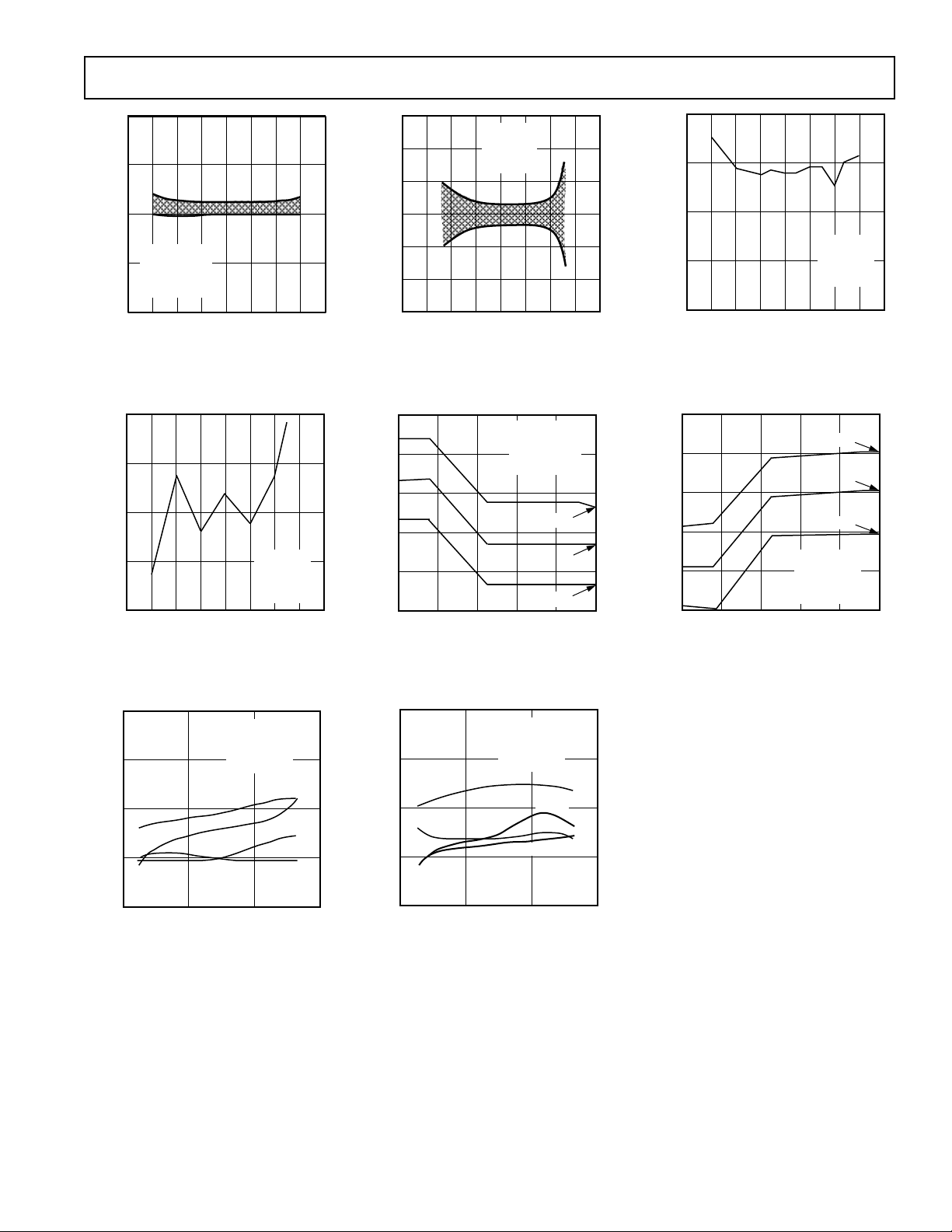
Figure 7. DNL vs. V
LSB
–
+1
ERROR
0
LINEARITY
–1
MAXIMUM
123
V
REFH
Figure 10. INL vs. V
V
REFH
–
–
Volts
Volts
REFH
V
DD
V
SS
V
REFL
T
A
REFH
1110987
=
=
+5V
=
0V
=
+25ⴗC
0
–1
–2
MAXIMUM LINEARITY ERROR – LSB
12
V
REFH
– Volts
Figure 8. DNL vs. V
321
REFH
0.4
V
=
+15V
DD
=
–15V
V
SS
=
+10V
0.2
V
V
REFH
REFL
=
–10V
0
X+3
–0.2
X
FULL-SCALE ERROR – LSB
0V
–0.4
–0.6
0
T = HOURS OF OPERATION AT +125ⴗC
X–3
600400 800200
1000
Figure 11. Full-Scale Error vs.
Time Accelerated by Burn-In
0.2
VDD = +15V
V
1086 12
–
Volts
SS
V
REFL
= +25ⴗC
T
A
REFH
0.1
MAXIMUM LINEARITY ERROR – LSB
Figure 9. INL vs. V
V
REFH
0.3
X+3
0.1
–0.1
–0.3
–0.5
ZERO-SCALE ERROR – LSB
–0.7
0
T = HOURS OF OPERATION AT +125ⴗC
X–3
V
= +15V
DD
= –15V
V
SS
= +10V
V
REFH
= –10V
V
REFL
600400 800200
Figure 12. Zero-Scale Error vs.
Time Accelerated by Burn-In
= –15V
= 0V
X
1000
0.2
V
= +15V
DD
= –15V
V
SS
= +10V
V
V
REFH
REFL
= –10V
–0.2
–0.4
FULL-SCALE ERROR – LSB
0
DAC A
–0.6
TEMPERATURE – ⴗC
Figure 13. Full-Scale Error vs.
Temperature
DAC D
DAC B
DAC C
0.3
V
=
+15V
DD
=
–15V
V
SS
=
+10V
V
0.1
V
REFH
REFL
=
–10V
DAC A
–0.1
DAC C
DAC D
–0.3
ZERO-SCALE ERROR – LSB
–0.5
150–75 750
–75
TEMPERATURE – ⴗC
DAC B
750
150
Figure 14. Zero-Scale Error vs.
Temperature
REV. D
–7–
DAC8412/DAC8413
0.37500
0.26125
0.18750
0.08375
0
–0.09375
LINEARITY ERROR – LSB
–0.18750
–0.23125
–0.37500
V
REFH
V
REFL
T
= +25ⴗC
A
0 4096512
= +10V
= 0V
1024 1536 2048 2560 3072 3584
DIGITAL INPUT CODE – Decimal
Figure 15. Channel-to-Channel Matching
SUPPLY
0
= ±15 V)
(V
1.00
0.75
0.50
0.25
–0.25
VDD = +5.0V
V
= 0V
SS
V
= +2.5V
REFH
T
= +25ⴗC
A
–0.125
LINEARITY ERROR – LSB
–0.250
–0.375
–0.500
– mA
I
0.500
0.375
0.250
0.125
2.0
1.5
1.0
0.5
VREFH
0
VDD = +15V
= –15V
V
SS
= +10V
V
REFH
= –10V
V
REFL
= –55ⴗC, +25ⴗC, +125ⴗC
T
A
0 4096512
VDD = +15V
V
= –15V
SS
V
= +10V
REFH
V
= –10V
REFL
T
= +25ⴗC
A
1024 1536 2048 2560 3072 3584
DIGITAL INPUT CODE – Decimal
Figure 18. INL vs. Code
LINEARITY ERROR – LSB
–0.50
–0.75
–1.00
0 4096512
1024 1536 2048 2560 3072 3584
DIGITAL INPUT CODE – Decimal
Figure 16. Channel-to-Channel Matching
= +5 V/GND)
SUPPLY
7
4
–713–3
Figure 17. I
V
=
DD
=
V
SS
V
REFL
159
V
– Volts
REFH
DD
vs. V
All DACs High
REFH
– mA
DD
I
(V
13
10
+15V
–15V
=
–10V
0
–0.5
0 4095511
1023 1535 2047 2559 3071 3583
DIGITAL INPUT CODE – Decimal
Figure 19. I
VREFH
vs. Code
–8–
REV. D

DAC8412/DAC8413
32.5mV
+5V
INPUT
0
5mV/DIV
V
5
DIV
TRIG'D
–17.5mV
–1.96s
1 LSB ERROR BAND
V
=
+15V
DD
V
=
–15V
SS
V
=
+10V
REFH
V
=
–10V
REFL
T
=
+25ⴗC
A
2s/DIV 18.04s
Figure 20. Settling Time (Positive)
10V
1V/
DIV
EA
TRIG'D
V
V
V
V
T
DD
SS
REFH
REFL
=
A
=
=
+25ⴗC
+15V
–15V
=
=
+10V
–10V
15.5mV
INPUT
–5V
0
V
V
V
V
T
DD
SS
REFH
REFL
A
=
=
=
+25ⴗC
+15V
–15V
=
=
–10V
+10V
2mV/DIV
V
5
DIV
TRIG'D
–4.5mV
–1.96s
2s/DIV 18.04s
Figure 21. Settling Time (Negative)
1.0
VDD = +15V
V
= –15V
SS
0.8
V
= +10V
REFH
V
= –10V
REFL
T
= +25ⴗC
0.6
A
0.4
INL – LSB
0.2
0.0
10V
1V/
DIV
EA
TRIG'D
0V
–580ns
V
DD
V
SS
V
REFH
V
REFL
T
A
1s/DIV 9.42s
Figure 22. Positive Slew Rate
12
VDD = +15V
V
= –15V
SS
10
V
= +10V
REFH
V
= –10V
REFL
T
= +25ⴗC
8
A
6
4
FULL SCALE VOLTAGE – V
2
=
=
=
+25ⴗC
+15V
–15V
=
=
+10V
–10V
0V
–580ns
1s/DIV 9.42s
Figure 23. Negative Slew Rate
0
–10
VDD = +15V
–30
GAIN – dB
V
V
V
–50
DATA BITS = +5V
200mV p-p
= –15V
SS
= 0 ⴞ100mV
REFH
= –10V
REFL
10M1001M100k10k1k100
FREQUENCY – Hz
Figure 26. Small Signal Response
–0.2
LOAD RESISTANCE – K⍀
1000.01 10.01.000.10
Figure 24. DAC 8412 INL vs. Load
Resistance
10
I
6
V
=
+15V
DD
V
=
–15V
SS
DD
2
–2
I
SS
750
150
POWER SUPPLY CURRENT – mA
–10
–6
–75
TEMPERATURE – ⴗC
Figure 27. Power Supply Current vs.
Temperature
0
LOAD RESISTANCE – K⍀
1000.01 10.01.000.10
Figure 25. DAC 8412 Output Swing
vs. Load Resistance
100
+PSRR
80
–PSRR
60
+PSRR:
V
= +15Vⴞ1Vp
DD
40
= –15V
V
SS
–PSRR:
= +15V
V
DD
20
= –15Vⴞ1V
V
SS
POWER SUPPLY REJECTION – dB
0
V
REFH
ALL DATA 0
10
= 10V
100
FREQUENCY – Hz
1M
100k10k1k
Figure 28. PSRR vs. Frequency
REV. D
–9–

DAC8412/DAC8413
OU
10.0
1.00
0.10
NOISE DENSITY – V
0.01
0.001
NOISE FREQUENCY – Hz
Figure 29. DAC8412 Noise
Frequency vs. Noise Density
VDD = +15V
V
= –15V
SS
V
REFH
V
REFL
T
= +25ⴗC
A
25
20
15
10
5
– mA
0
OUT
I
–5
–10
–15
–20
–25
0
– Volts
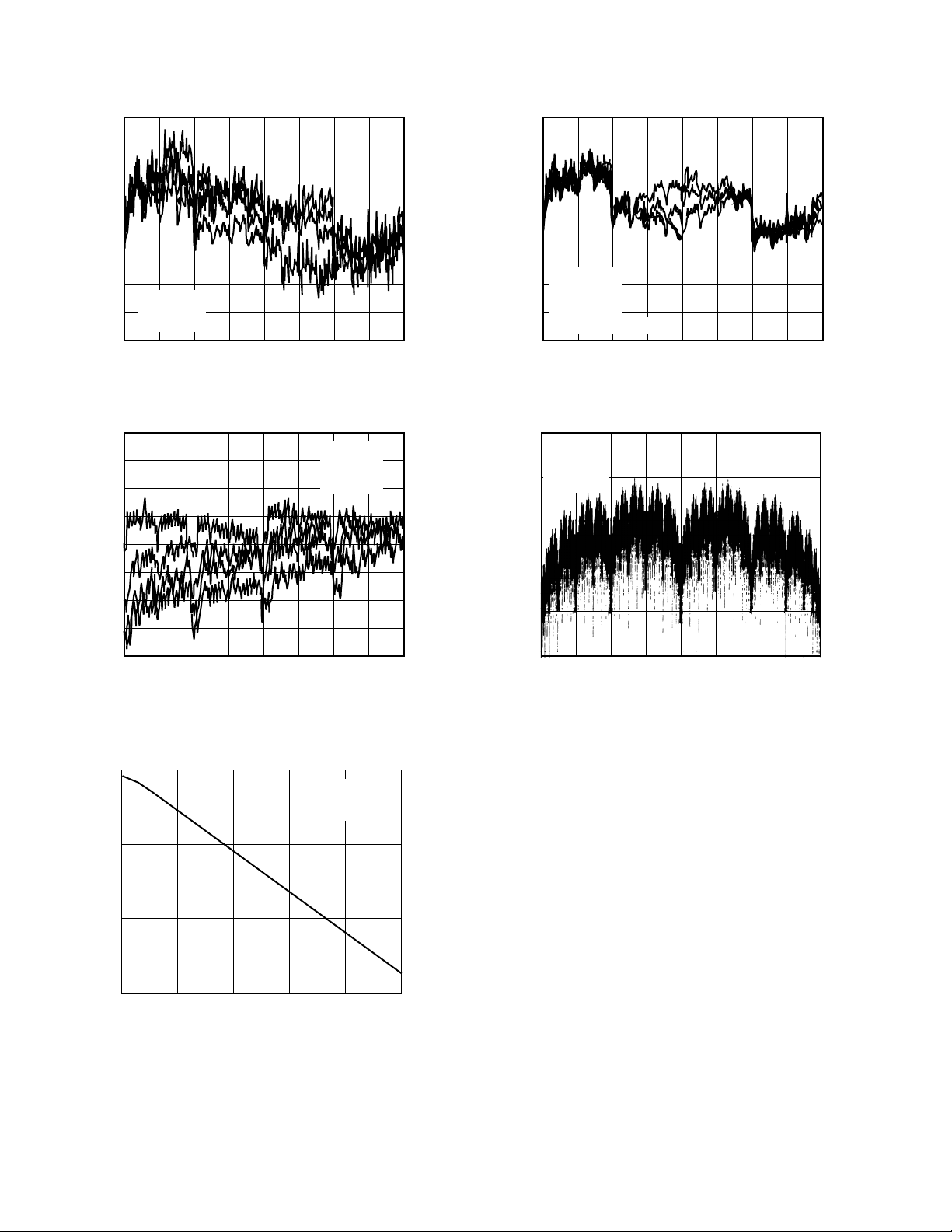
T
OUT
30
20
10
– mA
0
OUT
I
–10
–20
–30
0
–25 –20
+I
SC
vs. V
= +10V
= –10V
100001 100010010
VDD = +15V
V
= 0V
SS
V
= +10V
REFH
V
= 0V
REFL
T
= +25ⴗC
A
DATA = 800
H
–I
SC
–4 –20 2 4
V
Figure 32. I
V
= +15V
DD
= –15V
V
SS
= +10V
V
REFH
= –10V
V
REFL
= +25ⴗC
T
A
DATA = 000
H
–I
SC
V
Figure 30. I
6–6
OUT
+I
SC
1
20uV/DIV
25
OUT
– Volts
OUT
vs. V
2
1
20151050–5–10–15
OUT
DEGLITCHER OUTPUT
1V
Figure 31. Broadband Noise
10s
4s1V
GLITCH AT DAC OUTPUT
CH2 1.86V
Figure 33. Glitch and Deglitched Results
VDD = +15V
V
V
V
T
M 200s A CH1 12.9mV
CH1 MEAN
66.19V
= –15V
SS
= +10V
REFH
= –10V
REFL
= +25ⴗC
A
OPERATION
Introduction
The DAC8412 and DAC8413 are quad, voltage output, 12-bit
parallel input DACs featuring a 12-bit data bus with readback
capability. The only differences between the DAC8412 and
DAC8413 are the reset functions. The DAC8412 resets to midscale (code 800
(code 000
) and the DAC8413 resets to minimum scale
H
).
H
The ability to operate from a single +5 V supply is a unique feature of these DACs.
Operation of the DAC8412 and DAC8413 can be viewed by
dividing the system into three separate functional groups: the
digital I/O and logic, the digital to analog converters and the output
amplifiers.
DACs
Each DAC is a voltage switched, high impedance (R = 50 kΩ),
R-2R ladder configuration. Each 2R resistor is driven by a pair of
switches that connect the resistor to either V
REFH
or V
REFL
.
Glitch
Worst-case glitch occurs at the transition between half-scale
digital code 1000 0000 0000 to half-scale minus 1 LSB, 0111
1111 1111. It can be measured at about 2 V µs. (See Figure 33.)
For demanding applications such as waveform generation or
precision instrumentation control, a deglitcher circuit can be
implemented with a standard sample-and-hold circuit. (See
Figure 34.) When CS is enabled by synchronizing the hold
period to be longer than the glitch tradition, the output voltage
can be smoothed with minimum disturbance. A quad sampleand-hold amplifier, SMP04, has been used to illustrate the
deglitching result. (See Figure 33.)
DACOUT
S/H
DACOUT
CS
HSH
DACOUT'
DACOUT'
SS/H
Figure 34. Deglitcher Circuit
–10–
REV. D

DAC8412/DAC8413
Reference Inputs
All four DACs share common reference high (V
ence low (V
) inputs. The voltages applied to these reference
REFL
) and refer-
REFH
inputs set the output high and low voltage limits of all four of
the DACs. Each reference input has voltage restrictions with
respect to the other reference and to the power supplies. The
can be set at any voltage between VSS and V
V
REFL
and V
V
REFL
can be set to any value between +VDD – 2.5 V and
REFH
+ 2.5 V. Note that because of these restrictions the
DAC8412 references cannot be inverted (i.e., V
greater than V
It is important to note that the DAC8412’s V
REFH
).
REFH
sinks and sources current. Also the input current of both V
and V
are code dependent. Many references have limited
REFL
REFH
cannot be
REFL
input both
– 2.5 V,
REFH
current sinking capability and must be buffered with an amplifier to drive V
REFH
. The V
has no such special requirements.
REFL
It is recommended that the reference inputs be bypassed with
0.2 µF capacitors when operating with ± 10 V references. This
limits the reference bandwidth.
Digital I/O
See Table I for digital control logic truth table. Digital I/O consists
of a 12-bit bidirectional data bus, two registers select inputs, A0
and A1, a R/W input, a RESET input, a Chip Select (CS), and
a Load DAC (LDAC) input. Control of the DACs and bus
direction is determined by these inputs as shown in Table I.
Digital data bits are labeled with the MSB defined as data bit
“11” and the LSB as data bit “0.” All digital pins are TTL/
CMOS compatible.
See Figure 35 for a simplified I/O logic diagram. The register
select inputs A0 and A1 select individual DAC registers “A”
(binary code 00) through “D” (binary code 11). Decoding of
the registers is enabled by the CS input. When CS is high no
decoding takes place, and neither the writing nor the reading of
the input registers is enabled. The loading of the second bank of
registers is controlled by the asynchronous LDAC input. By taking LDAC low while CS is enabled, all output registers can be
updated simultaneously. Note that the t
required pulsewidth
LDW
for updating all DACs is a minimum of 170 ns.
The R/W input, when enabled by CS, controls the writing to and
reading from the input register.
Coding
Both the DAC8412 and DAC8413 use binary coding. The output voltage can be calculated by:
VV
=+
OUT REFL
VV N
REF H REFL
4096
×(_)
where N is the digital code in decimal.
RESET
The RESET function can be used either at power-up or at any
time during the DAC’s operation. The RESET function is independent of CS. This pin is active LOW and sets the DAC output
registers to either center code for the DAC8412, or zero code
for the DAC8413. The reset to center code is most useful when
the DAC is configured for bipolar references and an output of
zero volts after reset is desired.
Supplies
Supplies required are VSS, VDD and V
be set between –15 V and 0 V. V
DD
. The VSS supply can
LOGIC
is the positive supply; its op-
erating range is between +5 V and +15 V.
V
is the digital output supply voltage for the readback
LOGIC
function. It is normally connected to +5 V. This pin is a logic
reference input only. It does not supply current to the device.
If you are not using the readback function, V
circuit. While V
does not supply current to the DAC8412,
LOGIC
can be left open-
LOGIC
it does supply currents to the digital outputs when readback
is used.
Amplifiers
Unlike many voltage output DACs, the DAC8412 features buffered voltage outputs. Each output is capable of both sourcing
and sinking 5 mA at ±10 volts, eliminating the need for external
amplifiers when driving 500 pF or smaller capacitive load in
most applications. These amplifiers are short-circuit protected.
Table I. DAC8412/DAC8413 Logic Table
A1 A0 R/W CS RS LDAC INPUT REG OUTPUT REG MODE DAC
L L L L H L WRITE WRITE Transparent A
L H L L H L WRITE WRITE Transparent B
H L L L H L WRITE WRITE Transparent C
H H L L H L WRITE WRITE Transparent D
LLLLH H WRITE HOLD WRITE INPUTA
LHLLH H WRITE HOLD WRITE INPUTB
H L L L H H WRITE HOLD WRITE INPUT C
H H L L H H WRITE HOLD WRITE INPUT D
L L H L H H READ HOLD READ INPUT A
L H H L H H READ HOLD READ INPUT B
H L H L H H READ HOLD READ INPUT C
H H H L H H READ HOLD READ INPUT D
X X X H H L HOLD Update all output registers All
X X X H H H HOLD HOLD HOLD All
X X X X L X *All registers reset to mid/zero-scale All
XXXHg X *All registers latched to mid/zero-scale All
*DAC8412 resets to midscale, and DAC8413 resets to zero scale. L = Logic Low; H = Logic High; X - Don’t Care. Input and Output registers are transparent when
asserted.
REV. D
–11–

DAC8412/DAC8413
V
REFHVDDVSS
CS
R/W
DB11..DB0
V
LOGIC
A0
A1
READBACK
DATAOUT_DB11
DGND
RDDACA
WRDACA
RDDACB
WRDACB
REGISTER
RDDACC
WRDACC
RDDACD
WRDACD
READOUTBAR
READBACKDATAIN_DB11
INPUT
WRDB0
WRDB1
WRDB2
WRDB3
WRDB4
WRDB5
WRDB6
WRDB7
WRDB8
WRDB9
WRDB10
WRDB11
READBACKDATAIN_DB10
Figure 35. Simplified I/O Logic Diagram
OUTPUT
REGISTER
READOUT
DAC A
DAC B
DAC C
DAC D
V
OUTA
V
OUTB
V
OUTC
V
OUTD
V
REFL
LDAC
RESET
Careful attention to grounding is important to accurate operation of the DAC8412. This is not because the DAC8412 is
more sensitive than other 12-bit DACs, but because with four
outputs and two references there is greater potential for ground
loops. Since the DAC8412 has no analog ground, the ground
must be specified with respect to the reference.
Reference Configurations
Output voltage ranges can be configured as either unipolar or
bipolar, and within these choices a wide variety of options exists.
The unipolar configuration can be either positive or negative
voltage output, and the bipolar configuration can be either symmetrical or nonsymmetrical.
INPUT
+15V
REF10
+
OUTPUT
TRIM
OP400
10k⍀
+10V OPERATION
OP-400
0.2F
V
V
REFH
REFL
+15V
V
DD
DAC8412
OR
DAC8413
V
SS
–15V
0.1F
//10F
Figure 36. Unipolar +10 V Operation
+15V
GAIN
100k⍀
BALANCE
100k⍀
AD688
AD588
39k⍀
FOR ⴞ10V
FOR ⴞ 5V
6.2⍀
0.2F
6.2⍀
0.2F
1F
ⴞ5 OR ⴞ10V OPERATION
+15V
V
DD
V
REFH
DAC8412
OR
DAC8413
V
REFL
V
SS
–15V
0.1F
//10F
Figure 37. Symmetrical Bipolar Operation
Figure 37 (Symmetrical Bipolar Operation) shows the DAC8412
configured for ±10 V operation. Note: See the AD688 data
sheet for a full explanation of reference operation. Adjustments may
not be required for many applications since the AD688 is a very
high accuracy reference. However if additional adjustments are
required, adjust the DAC8412 full scale first. Begin by loading
the digital full-scale code (FFF
), and then adjust the Gain
H
Adjust potentiometer to attain a DAC output voltage of 9.9976 V.
Then, adjust the Balance Adjust to set the center scale output
voltage to 0.000 V.
–12–
REV. D

DAC8412/DAC8413
The 0.2 µF bypass capacitors shown at the reference inputs
in Figure 37 should be used whenever ±10 V references are
used. Applications with single references or references to ±5 V
may not require the 0.2 µF bypassing. The 6.2 Ω resistor in series
with the output of the reference amplifier is to keep the amplifier
from oscillating with the capacitive load. We have found that this is
large enough to stabilize this circuit. Larger resistor values are
acceptable, provided that the drop across the resistor doesn’t
exceed a V
. Assuming a minimum VBE of 0.6 V and a maxi-
BE
mum current of 2.75 mA, then the resistor should be under
200 Ω for the loading of a single DAC8412.
Using two separate references is not recommended. Having two
references could cause different drifts with time and temperature; whereas with a single reference, most drifts will track.
Unipolar positive full-scale operation can usually be set with a
reference with the correct output voltage. This is preferable to
using a reference and dividing down to the required value. For a
10 V full-scale output, the circuit can be configured as shown
in Figure 38. In this configuration the full-scale value is set first
by adjusting the 10 kΩ resistor for a full-scale output of 9.9976 V.
10k⍀
V
DD
DAC8412
OR
DAC8413
V
SS
0.1F
//10F
GND
–15V
TRIM
REF08
0.01F
10F
OUTPUT
0.2F
ZERO
V
REFH
V
REFL
TO
–10V OPERATION
Figure 38 shows the DAC8412 configured for –10 V to 0 V
operation. A REF08 with a –10 V output is connected directly
to V
for the reference voltage.
REFL
Single +5 V Supply Operation
For operation with a +5 V supply, the reference voltage should be
set between 1.0 V and +2.5 V for optimum linearity. Figure
39 shows a REF43 used to supply a +2.5 V reference voltage.
The headroom of the reference and DAC are both sufficient to
support a +5 V supply with ± 5% tolerance. VDD and V
LOGIC
should be connected to the same supply. Separate bypassing
to each pin should also be used.
+5V
10F
0.01F
REF43
GND
INPUT
OUTPUT
TRIM
10k⍀
ZERO TO +2.5V OPERATION
SINGLE +5V SUPPLY
V
0.2F
V
REFH
REFL
V
DD
DAC8412
OR
DAC8413
V
SS
0.1F
//10F
Figure 39. +5 V Single Supply Operation
Figure 38. Unipolar –10 V Operation
REV. D
–13–

DAC8412/DAC8413
0.458 (11.63)
0.442 (11.23)
SQ
TOP
VIEW
0.048 (1.21)
0.042 (1.07)
0.020
(0.50)
OUTLINE DIMENSIONS
Dimensions shown in inches and (mm).
28-Position Leadless Chip Carrier
(TC Suffix)
R TYP
0.075
(1.91)
REF
0.075
(1.91)
REF
0.055 (1.40)
0.045 (1.14)
0.458
(11.63)
MAX
SQ
0.100 (2.54)
0.064 (1.63)
0.095 (2.41)
0.075 (1.90)
0.011 (0.28)
0.007 (0.18)
0.088 (2.24)
0.054 (1.37)
28-Lead PLCC (P-28A)
(PC Suffix)
0.180 (4.57)
0.050
(1.27)
BSC
0.165 (4.19)
0.110 (2.79)
0.085 (2.16)
0.048 (1.21)
0.042 (1.07)
4
5
11
12
0.456 (11.58)
R
0.450 (11.43)
0.495 (12.57)
0.485 (12.32)
PIN 1
IDENTIFIER
TOP VIEW
(PINS DOWN)
0.056 (1.42)
0.042 (1.07)
26
25
19
18
SQ
SQ
26
25
19
18
0.300 (7.62)
BSC
0.150
(3.51)
BSC
28
1
BOTTOM
VIEW
0.025 (0.63)
0.015 (0.38)
0.021 (0.53)
0.013 (0.33)
0.032 (0.81)
0.026 (0.66)
0.040 (1.01)
0.025 (0.64)
0.200
(5.08)
BSC
11
0.015 (0.38)
MIN
4
5
0.028 (0.71)
0.022 (0.56)
0.050
(1.27)
BSC
12
45ⴗ TYP
0.430 (10.92)
0.390 (9.91)
C1544a–2–3/00 (rev. D)
PIN 1
0.250
(6.35)
MAX
0.200 (5.05)
0.125 (3.18)
28-Lead Epoxy DIP (N-28)
(P Suffix)
1.565 (39.70)
1.380 (35.10)
28
114
0.022 (0.558)
0.014 (0.356)
0.100
(2.54)
BSC
15
0.060 (1.52)
0.015 (0.38)
0.070
(1.77)
MAX
0.580 (14.73)
0.485 (12.32)
0.150
(3.81)
MIN
SEATING
PLANE
0.625 (15.87)
0.600 (15.24)
–14–
0.195 (4.95)
0.125 (3.18)
0.015 (0.381)
0.008 (0.204)
PRINTED IN U.S.A.
REV. D
 Loading...