Analog Devices DAC8413FP, DAC8413EP, DAC8413BTC, DAC8412FPC, DAC8412FP Datasheet
...
Quad, 12-Bit DAC
a
FEATURES
+5 V to ⴞ15 V Operation
Unipolar or Bipolar Operation
True Voltage Output
Double-Buffered Inputs
Reset to Min (DAC8413) or Center Scale (DAC8412)
Fast Bus Access Time
Readback
APPLICATIONS
Automatic Test Equipment
Digitally Controlled Calibration
Servo Controls
Process Control Equipment
GENERAL DESCRIPTION
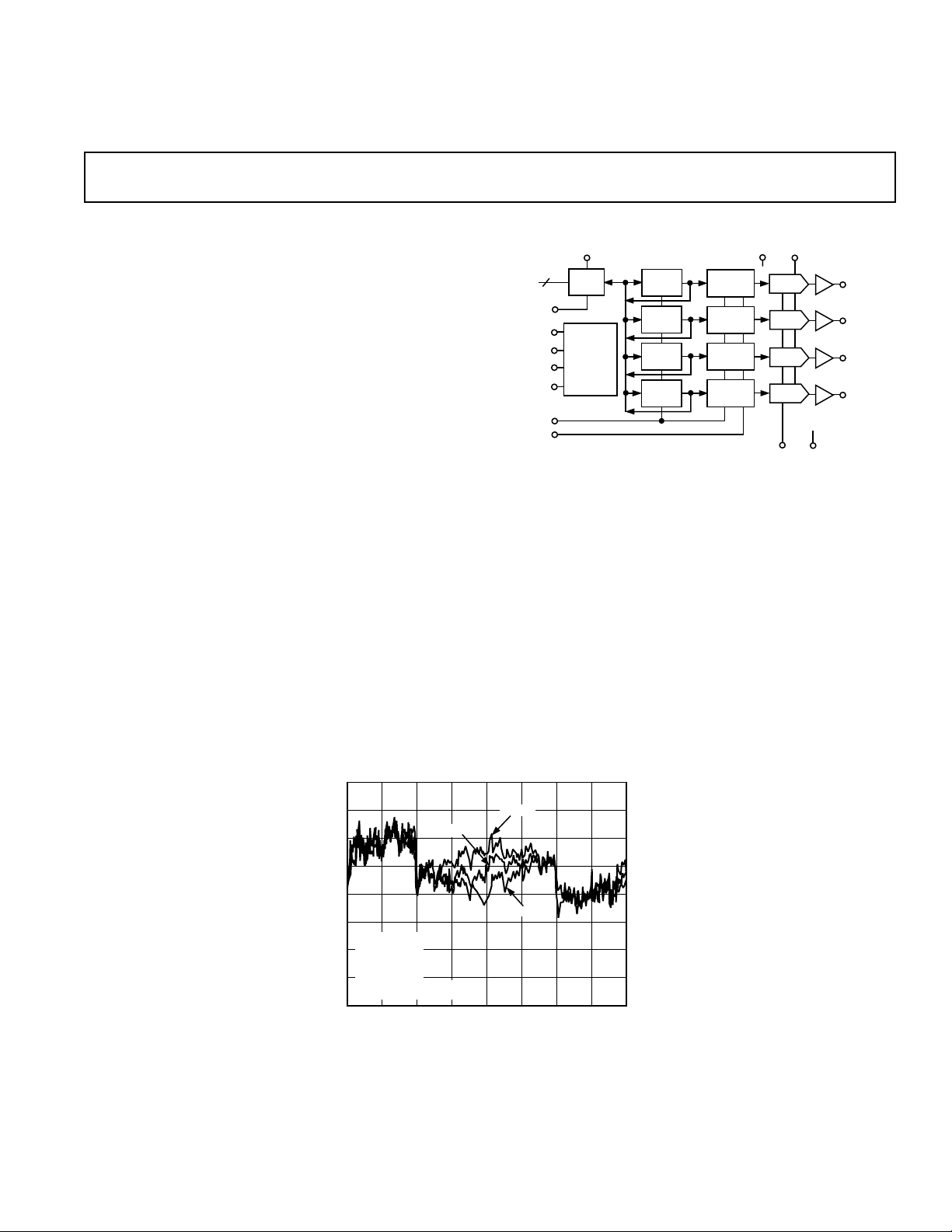
The DAC8412 and DAC8413 are quad, 12-bit voltage output
DACs with readback capability. Built using a complementary
BiCMOS process, these monolithic DACs offer the user very
high package density.
Output voltage swing is set by the two reference inputs V
and V
. By setting the V
REFL
input to 0 V and V
REFL
positive voltage, the DAC will provide a unipolar positive output
range. A similar configuration with V
at 0 V and V
REFH
a negative voltage will provide a unipolar negative output range.
Bipolar outputs are configured by connecting both V
to nonzero voltages. This method of setting output voltage
V
REFL
range has advantages over other bipolar offsetting methods because
it is not dependent on internal and external resistors with different
temperature coefficients.
REFH
REFH
to a
REFL
and
REFH
at
Voltage Output with Readback
DAC8412/DAC8413
FUNCTIONAL BLOCK DIAGRAM
V
LOGIC
12
CS
A0
A1
I/O
PORT
CONTROL
LOGIC
INPUT
REG
INPUT
REG B
INPUT
REG C
INPUT
REG D
OUTPUT
A
REG
OUTPUT
REG B
OUTPUT
REG C
OUTPUT
REG D
DATA
I/O
DGND
RESET
LDAC
R/W
Digital controls allow the user to load or read back data from any
DAC, load any DAC and transfer data to all DACs at one time.
An active low RESET loads all DAC output registers to midscale for the DAC8412 and zero scale for the DAC8413.
The DAC8412/DAC8413 are available in 28-lead plastic DIP,
PLCC and LCC packages. They can be operated from a wide
variety of supply and reference voltages with supplies ranging
from single +5 V to ±15 V, and references from +2.5 V to ±10 V.
Power dissipation is less than 330 mW with ±15 V supplies and
only 60 mW with a +5 V supply.
For MIL-STD-883 applications, contact your local ADI sales
office for the DAC8412/DAC8413/883 data sheet which specifies
operation over the –55°C to +125°C temperature range. All
883 parts are also available on Standard Military Drawings
5962-91 76401MXA through 76404M3A.
V
V
REFH
DD
A
DAC
A
DAC B
DAC C
DAC
D
V
REFLVSS
V
V
V
V
OUTA
OUTB
OUTC
OUTD
0.500
0.375
0.250
0.125
0
–0.125
–0.250
–0.375
–0.500
VDD = +15V
V
= –15V
SS
V
= +10V
REFH
V
= –10V
REFL
T
= –55ⴗC, +25ⴗC, +125ⴗC
A
0 4096512
LINEARITY ERROR – LSB
+25ⴗC
1024 1536 2046 2548 2560 3072
DIGITAL INPUT CODE – Decimal
Figure 1. INL vs. Code Over Temperature
REV. D
Information furnished by Analog Devices is believed to be accurate and
reliable. However, no responsibility is assumed by Analog Devices for its
use, nor for any infringements of patents or other rights of third parties
which may result from its use. No license is granted by implication or
otherwise under any patent or patent rights of Analog Devices.
+125ⴗC
–55ⴗC
One Technology Way, P.O. Box 9106, Norwood, MA 02062-9106, U.S.A.
Tel: 781/329-4700 World Wide Web Site: http://www.analog.com
Fax: 781/326-8703 © Analog Devices, Inc., 2000

DAC8412/DAC8413–SPECIFICATIONS
(@ V
= +15.0 V, VSS = –15.0 V, V
DD
ELECTRICAL CHARACTERISTICS
–40ⴗC ≤ TA ≤ +85ⴗC unless otherwise noted. See Note 1 for supply variations.)
Parameter Symbol Conditions Min Typ Max Units
Integral Nonlinearity Error INL E Grade 0.25 ±0.5 LSB
INL F Grade ± 1 LSB
Differential Nonlinearity Error DNL Monotonic Over Temperature –1 LSB
Min-Scale Error V
Full-Scale Error V
ZSE
FSE
Min-Scale Tempco TCV
Full-Scale Tempco TCV
RL = 2 kΩ±2 LSB
RL = 2 kΩ±2 LSB
RL = 2 kΩ 15 ppm/°C
ZSE
RL = 2 kΩ 20 ppm/°C
FSE
Linearity Matching Adjacent DAC Matching ± 1 LSB
REFERENCE
Positive Reference Input Voltage Range Note 2 V
Negative Reference Input Voltage Range Note 2 –10 V
Reference High Input Current I
Reference Low Input Current I
Large Signal Bandwidth BW –3 dB, V
REFH
REFL
= 0 V to +10 V p-p 160 kHz
REFH
AMPLIFIER CHARACTERISTICS
Output Current I
Settling Time t
OUT
S
RL = 2 kΩ, CL = 100 pF –5 +5 mA
to 0.01%, 10 V Step, RL = 1 kΩ 10 µs
Slew Rate SR 10% to 90% 2.2 V/µs
Analog Crosstalk 72 dB
LOGIC CHARACTERISTICS
Logic Input High Voltage V
Logic Input Low Voltage V
Logic Output High Voltage V
Logic Output Low Voltage V
Logic Input Current I
Input Capacitance C
Digital Feedthrough
LOGIC TIMING CHARACTERISTICS
3
3
Chip Select Write Pulsewidth t
Write Setup t
Write Hold t
Address Setup t
Address Hold t
Load Setup t
Load Hold t
Write Data Setup t
Write Data Hold t
Load Data Pulsewidth t
Reset Pulsewidth t
Chip Select Read Pulsewidth t
Read Data Hold t
Read Data Setup t
Data to Hi Z t
Chip Select to Data t
INH
INL
OH
OL
IN
IN
WCS
WS
WH
AS
AH
LS
LH
WDS
WDH
LDW
RESET
RCS
RDH
RDS
DZ
CSD
TA = +25°C2.4 V
TA = +25°C 0.8 V
IOH = +0.4 mA 2.4 V
IOL = –1.6 mA 0.4 V
V
= +2.5 V, V
REFH
REFL
Note 4
t
= 80 ns 0 ns
WCS
t
= 80 ns 0 ns
WCS
t
= 80 ns 20 ns
WCS
t
= 80 ns 0 ns
WCS
t
= 130 ns 0 ns
RCS
t
= 130 ns 0 ns
RCS
CL = 10 pF 200 ns
CL = 100 pF 160 ns
SUPPLY CHARACTERISTICS
Power Supply Sensitivity PSS 14.25 V ≤ V
Positive Supply Current I
Negative Supply Current I
Power Dissipation P
NOTES
1
All supplies can be varied ± 5%, and operation is guaranteed. Device is tested with nominal supplies.
2
Operation is guaranteed over this reference range, but linearity is neither tested nor guaranteed.
3
All parameters are guaranteed by design.
4
All input control signals are specified with tr = tf = 5 ns (10% to 90% of +5 V) and timed from a voltage level of 1.6 V.
Specifications subject to change without notice.
DD
SS
DISS
V
= +2.5 V 8.5 12 mA
REFH
≤ 15.75 V 150 ppm/V
DD
= +5.0 V, V
LOGIC
= +10.0 V, V
REFH
+ 2.5 VDD – 2.5 V
REFL
= –10.0 V,
REFL
REFH
– 2.5 V
–2.75 +1.5 +2.75 mA
0 +2 +2.75 mA
1 µA
8pF
= 0 V 5 nV-s
80 ns
0ns
0ns
70 ns
30 ns
170 ns
140 ns
130 ns
–10 –6.5 mA
330 mW
–2–
REV. D

DAC8412/DAC8413
(@ V
= V
= +5.0 V ⴞ 5%, VSS = 0.0 V, V
LOGIC
ELECTRICAL CHARACTERISTICS
DD
V
= –2.5 V, –40ⴗC ≤ TA ≤ +85ⴗC unless otherwise noted. See Note 1 for supply variations.)
REFL
Parameter Symbol Conditions Min Typ Max Units
Integral Nonlinearity Error INL E Grade 1/2 ± 1 LSB
INL F Grade ± 2 LSB
INL V
INL V
= 0.0 V; E Grade
SS
= 0.0 V; F Grade
SS
2
2
Differential Nonlinearity Error DNL Monotonic Over Temperature –1 LSB
Min-Scale Error V
Full-Scale Error V
Min-Scale Error V
Full-Scale Error V
ZSE
FSE
ZSE
FSE
Min-Scale Tempco TCV
Full-Scale Tempco TCV
VSS = –5.0 V ± 4 LSB
VSS = –5.0 V ± 4 LSB
VSS = 0.0 V ± 8 LSB
VSS = 0.0 V ± 8 LSB
ZSE
FSE
Linearity Matching Adjacent DAC Matching ±1 LSB
REFERENCE
Positive Reference Input Voltage Range Note 3 V
Negative Reference Input Voltage Range V
Reference High Input Current I
REFH
Large Signal Bandwidth BW –3 dB, V
= 0.0 V 0 V
SS
= –5.0 V –2.5 V
V
SS
Code 000H –1.0 +1.0 mA
= 0 V to 2.5 V p-p 450 kHz
REFH
AMPLIFIER CHARACTERISTICS
Output Current I
Settling Time t
OUT
S
RL = 2 kΩ, CL = 100 pF –1.25 +1.25 mA
to 0.01%, 2.5 V Step, RL = 1 kΩ 7 µs
Slew Rate SR 10% to 90% 2.2 V/µs
LOGIC CHARACTERISTICS
Logic Input High Voltage V
Logic Input Low Voltage V
Logic Output High Voltage V
Logic Output Low Voltage V
Logic Input Current I
Input Capacitance C
LOGIC TIMING CHARACTERISTICS
4
Chip Select Write Pulsewidth t
Write Setup t
Write Hold t
Address Setup t
Address Hold t
Load Setup t
Load Hold t
Write Data Setup t
Write Data Hold t
Load Data Pulsewidth t
Reset Pulsewidth t
Chip Select Read Pulsewidth t
Read Data Hold t
Read Data Setup t
Data to Hi Z t
Chip Select to Data t
INH
INL
OH
OL
IN
IN
WCS
WS
WH
AS
AH
LS
LH
WDS
WDH
LDW
RESET
RCS
RDH
RDS
DZ
CSD
TA = +25°C2.4 V
TA = +25°C0.8V
IOH = +0.4 mA 2.4 V
IOL = –1.6 mA 0.45 V
Note 5
t
= 150 ns 0 ns
WCS
t
= 150 ns 0 ns
WCS
t
= 150 ns 20 ns
WCS
t
= 150 ns 0 ns
WCS
t
= 170 ns 20 ns
RCS
t
= 170 ns 0 ns
RCS
CL = 10 pF 200 ns
CL = 100 pF 320 ns
SUPPLY CHARACTERISTICS
Power Supply Sensitivity PSS 100 ppm/V
Positive Supply Current I
Negative Supply Current I
Power Dissipation P
DD
SS
DISS
VSS = –5.0 V –10 mA
VSS = 0 V 60 mW
VSS = –5 V 110 mW
NOTES
1
All supplies can be varied ± 5%, and operation is guaranteed. Device is tested with VDD = +4.75 V.
2
For single supply operation only (V
3
Operation is guaranteed over this reference range, but linearity is neither tested nor guaranteed.
4
All parameters are guaranteed by design.
5
All input control signals are specified with tr = tf = 5 ns (10% to 90% of +5 V) and timed from a voltage level of 1.6 V.
Specifications subject to change without notice.
REV. D
= 0.0 V, VSS = 0.0 V): Due to internal offset errors, INL and DNL are measured beginning at code 2 (002H).
REFL
–3–
= +2.5 V, V
REFH
= 0.0 V, and VSS = –5.0 V ⴞ 5%,
REFL
± 2 LSB
± 4 LSB
100 ppm/°C
100 ppm/°C
+ 2.5 VDD – 2.5 V
REFL
REFH
REFH
– 2.5 V
– 2.5 V
1 µA
8pF
150 ns
0ns
0ns
70 ns
50 ns
180 ns
150 ns
170 ns
712 mA
DAC8412/DAC8413
t
CS
t
RDS
RCS
t
RDH
R/W
t
AS
t
AH
A0/A1
t
DATA
OUT
HI-Z HI -Z
t
CSD
DATA VALID
DZ
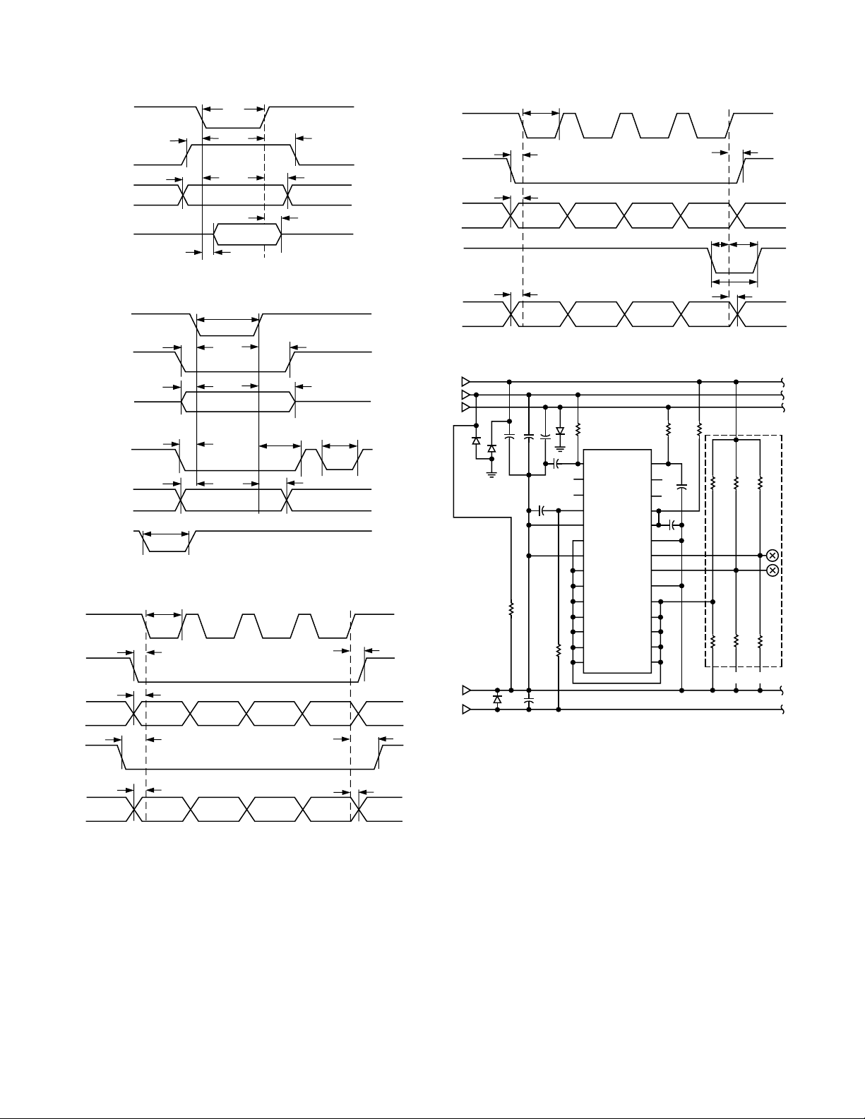
Figure 2. Data Output (Read Timing)
t
WCS
CS
t
WS
t
WH
R/W
t
AS
t
AH
A0/A1
t
t
LS
LH
t
LDW
LDAC
DATA
t
WDS
IN
t
RESET
t
WDH
RESET
Figure 3. Data WRITE (Input and Output Registers) Timing
80ns
CS
t
WH
t
LH
t
WDH
R/W
ADDRESS
LDAC
DATA
t
WS
t
AS
ADDRESS
ONE
IN
DATA1
VALID
t
t
LS
WDS
ADDRESS
TWO
DATA2
VALID
ADDRESS
THREE
DATA3
VALID
ADDRESS
FOUR
DATA4
VALID
CS
R/W
ADDRESS
LDAC
DATA IN
V
DD
V
REFH
V
REFL
DGND
V
SS
80ns
t
WS
t
AS
ADDRESS
ONE
DATA1
VALID
t
WDS
ADDRESS
TWO
DATA2
VALID
ADDRESS
THREE
DATA3
VALID
Figure 5. Double Buffer Mode
++
C1
C1
D1
C1
D1
C2
R6
D1
+
C1
V
= +15V, VSS = –15V, V
DD
R1
= 10⍀, R2 = 100⍀, R3 = 5k⍀, R4 = 10k⍀, R5 = 100k⍀,
R6 = 47⍀ FOR LCC, R6 = 100⍀ FOR DIP
C1 = 4.7F (ONCE PER PORT), C2 = 0.01F (EACH DEVICE)
D1 = 1N4001 OR EQUIVALENT (ONCE PER PORT)
R2
D1
+
C2
N/C
N/C
R1
V
V
V
V
V
DGND
RESET
LDAC
DB0
DB1
DB2
DB3
DB4
DB5
DB6 *
REFH
OUTB
OUTA
SS
REFH
REFL
V
OUTC
V
OUTD
V
DD
V
LOGIC
CS
A0
A1
R/W
DB11
DB10
DB9
DB8
DB7
= +10V, V
Figure 6. Burn-In Diagram
N/C
N/C
C2
REFL
ADDRESS
R2
C2
= 0V
FOUR
t
LS
DATA4
VALID
R1
R3
R5
ONCE PER PORT
t
LH
t
LDW
R3 R3
R4
t
t
WDH
WH
R4
Figure 4. Single Buffer Mode
–4–
REV. D
DAC8412/DAC8413
ABSOLUTE MAXIMUM RATINGS
(
TA = +25°C unless otherwise noted)
VSS to VDD . . . . . . . . . . . . . . . . . . . . . . . . . . . –0.3 V, +33.0 V
V
to V
SS
V
LOGIC
V
to V
SS
V
to VDD . . . . . . . . . . . . . . . . . . . . . . . . . +2.0 V, +33.0 V
REFH
to V
V
REFH
. . . . . . . . . . . . . . . . . . . . . . . . . –0.3 V, +33.0 V
LOGIC
to DGND . . . . . . . . . . . . . . . . . . . . . . –0.3 V, +7.0 V
. . . . . . . . . . . . . . . . . . . . . . . . –0.3 V, +VSS–2.0 V
REFL
. . . . . . . . . . . . . . . . . . . . . . . . +2.0 V, VSS–V
REFL
DD
Package Type JA* JCUnits
28-Lead Plastic DIP (P) 48 22 °C/W
28-Lead Hermetic Leadless Chip Carrier (TC) 70 28 °C/W
28-Lead Plastic Leaded Chip Carrier (PC) 63 25 °C/W
*θJA is specified for worst-case mounting conditions, i. e., θJA is specified for device
in socket.
Thermal Resistance
Current into Any Pin 4 . . . . . . . . . . . . . . . . . . . . . . . . ± 15 mA
Digital Input Voltage to DGND . . . . . –0.3 V, V
LOGIC
+0.3 V
Digital Output Voltage to DGND . . . . . . . . . . –0.3 V, +7.0 V
Operating Temperature Range
ET, FT, EP, FP, FPC . . . . . . . . . . . . . . . . –40°C to +85°C
AT, BT, BTC . . . . . . . . . . . . . . . . . . . . . –55°C to +125°C
Dice Junction Temperature . . . . . . . . . . . . . . . . . . . . . +150°C
Storage Temperature . . . . . . . . . . . . . . . . . . –65°C to +150°C
Power Dissipation Package . . . . . . . . . . . . . . . . . . . 1000 mW
Lead Temperature (Soldering, 60 sec) . . . . . . . . . . . . +300°C
ORDERING INFORMATION
1, 2
INL Military3 Temperature Extended Industrial3 Temperature Package Package
(LSB) –55ⴗC to +125ⴗC –40ⴗC to +85ⴗC Description Option
± 1 DAC8412FPC PLCC P-28A
± 1.5 DAC8412BTC/883 LCC E-28A
0.5 DAC8412EP Plastic DIP N-28
± 1 DAC8412FP Plastic DIP N-28
± 1 DAC8413FPC PLCC P-28A
± 1.5 DAC8413BTC/883 LCC E-28A
± 0.5 DAC8413EP Plastic DIP N-28
± 1 DAC8413FP Plastic DIP N-28
NOTES
1
Die Size 0.225 × 0.165 inches, 37,125 sq. mils (5.715 × 4.191 mm, 23.95 sq. mm). Substrate should be connected to VDD; Transistor Count = 2595.
2
Burn-in is available on extended industrial temperature range parts in cerdip.
3
A complete /883 data sheet is available. For availability and burn-in information, contact your local sales office.
CAUTION
1. Stresses above those listed under Absolute Maximum Ratings may cause permanent damage to the
device. This is a stress rating only; functional operation at or above this specification is not implied.
Exposure to the above maximum rating conditions for extended periods may affect
device reliability.
WARNING!
2. Digital inputs and outputs are protected, however, permanent damage may occur on unprotected units
from high-energy electrostatic fields. Keep units in conductive foam or packaging at all times until
ready to use. Use proper antistatic handling procedures.
3. Remove power before inserting or removing units from their sockets.
4. Analog outputs are protected from short circuit to ground or either supply.
REV. D
–5–
ESD SENSITIVE DEVICE
 Loading...