Analog Devices DAC8222 Datasheet
Dual 12-Bit Double-Buffered
a
FEATURES
Two Matched 12-Bit DACs on One Chip
Direct Parallel Load of All 12 Bits for High Data
Throughput
Double-Buffered Digital Inputs
12-Bit Endpoint Linearity (ⴞ1/2 LSB) Over Temperature
+5 V to +15 V Single Supply Operation
DACs Matched to 1% Max
Four-Quadrant Multiplication
Improved ESD Resistance
Packaged in a Narrow 0.3" 24-Lead DIP and 0.3"
24- Lead SOL Package
Available in Die Form
APPLICATIONS
Automatic Test Equipment
Robotics/Process Control/Automation
Digital Gain/Attenuation Control
Ideal for Battery-Operated Equipment
Multiplying CMOS D/A Converter
DAC8222
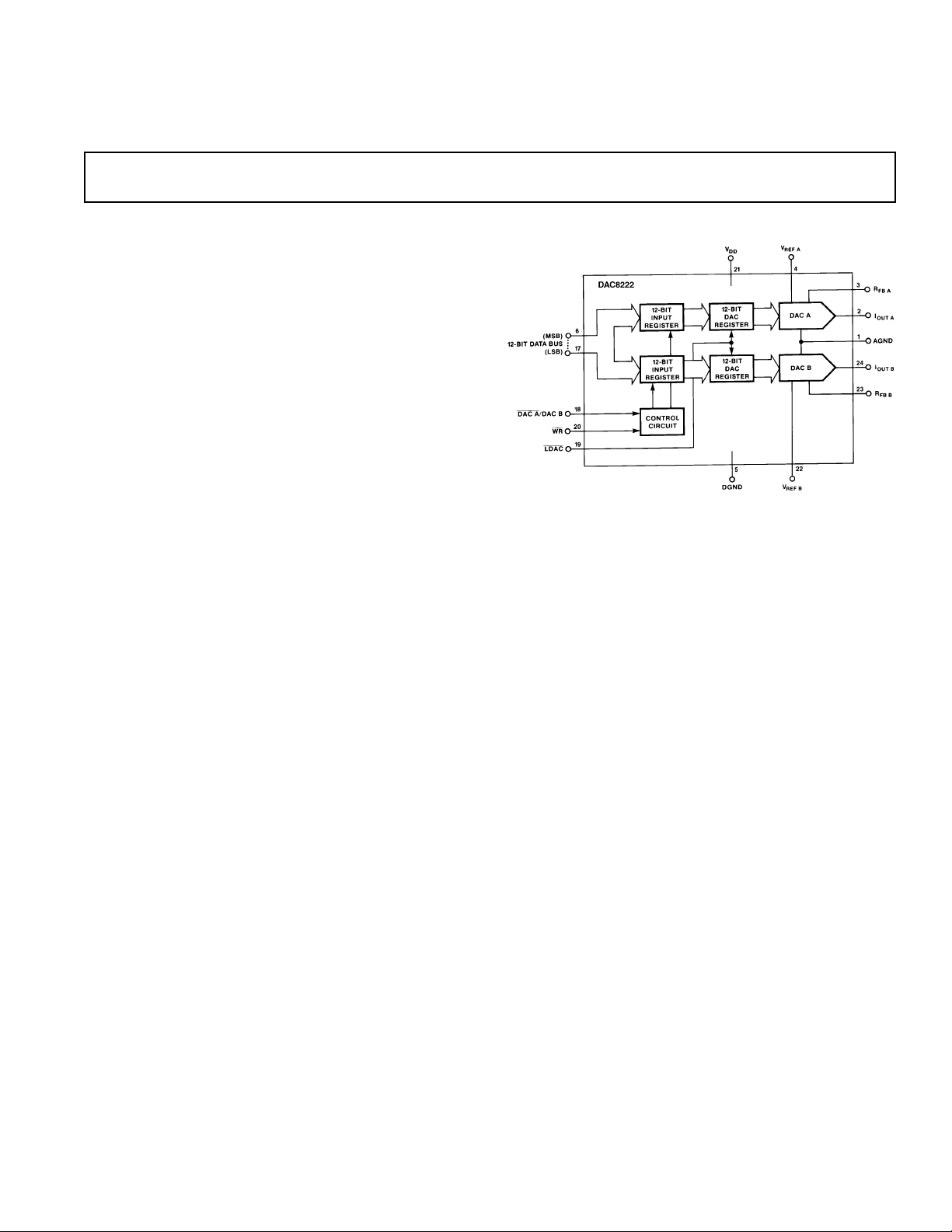
FUNCTIONAL DIAGRAM
GENERAL DESCRIPTION
The DAC8222 is a dual 12-bit, double-buffered, CMOS digitalto-analog converter. It has a 12-bit wide data port that allows a
12-bit word to be loaded directly. This achieves faster throughput time in stand-alone systems or when interfacing to a 16-bit
processor. A common 12-bit input TTL/CMOS compatible
data port is used to load the 12-bit word into either of the two
DACs. This port, whose data loading is similar to that of a RAM’s
write cycle, interfaces directly with most 12-bit and 16-bit bus
systems. (See DAC8248 for a complete 8-bit data bus interface
product.) A common bus allows the DAC8222 to be packaged
in a narrow 24-lead 0.3" DIP and save PCB space.
The DAC is controlled with two signals, WR and LDAC. With
logic low at these inputs, the DAC registers become transparent.
This allows direct unbuffered data to flow directly to either
DAC output selected by DAC A/DAC B. Also, the DAC’s
double-buffered digital inputs will allow both DACs to be
simultaneously updated.
DAC8222’s monolithic construction offers excellent DAC-toDAC matching and tracking over the full operating temperature range. The chip consists of two thin-film R-2R resistor
ladder networks, four 12-bit registers, and DAC control logic
circuitry. The device has separate reference-input and feedback
resistors for each DAC and operates on a single supply from
+5 V to +15 V. Maximum power dissipation at +5 V using
zero or V
The DAC8222 is manufactured with highly stable thin-film resistors on an advanced oxide-isolated, silicon-gate, CMOS
technology. Improved latch-up resistant design eliminates the
need for external protective Schottky diodes.
logic levels is less than 0.5 mW.
DD
REV. C
Information furnished by Analog Devices is believed to be accurate and
reliable. However, no responsibility is assumed by Analog Devices for its
use, nor for any infringements of patents or other rights of third parties
which may result from its use. No license is granted by implication or
otherwise under any patent or patent rights of Analog Devices.
One Technology Way, P.O. Box 9106, Norwood, MA 02062-9106, U.S.A.
Tel: 781/329-4700 World Wide Web Site: http://www.analog.com
Fax: 781/326-8703 © Analog Devices, Inc., 2000

DAC8222–SPECIFICATIONS
ELECTRICAL CHARACTERISTICS
(@ VDD = +5 V or +15 V, V
REF A
= V
= +10 V, V
REF B
OUT A
= V
= 0 V; AGND = DGND = 0 V;
OUT B
TA = Full Temperature Range Specified in Absolute Maximum Ratings; unless otherwise noted. Specifications apply for DAC A and DAC B.)
Parameter Symbol Conditions Min Typ Max Units
STATIC ACCURACY
Resolution N 12 Bits
Relative Accuracy INL Endpoint Linearity Error DAC8222A/E/G ±1/2 LSB
Differential Nonlinearity DNL All Grades are Guaranteed Monotonic ±1 LSB
Full-Scale Gain Error
1
G
DAC8222A/E ±1 LSB
FSE
DAC8222G ±2 LSB
DAC8222F/H ±4 LSB
Gain Temperature Coefficient
∆Gain/∆Temperature TCG
Output Leakage Current
(Pin 2), I
I
OUT A
(Pin 24) 0000 0000 0000 TA = Full Temp. Range ±50 nA
I
OUT B
Input Resistance
(V
REF A
, V
)R
REF B
Input Resistance Match
LKG
∆R
R
REF
REF
(Notes 2, 7) ±2 ±5 ppm/°C
FS
All Digital Inputs = TA = +25°C ±5 ±10 nA
(Note 9) 8 11 15 kΩ
REF
DIGITAL INPUTS
Digital Input High V
Digital Input Low V
Input Current I
Input Capacitance
2
INH
INL
IN
C
IN
VDD = +5 V 2.4 V
= +15 V 13.5 V
V
DD
VDD = +5 V 0.8 V
= +15 V 1.5 V
V
DD
VIN = 0 V or V
and V
INL
DB0–DB11 10 pF
or V
DD
INH
WR, LDAC, DAC A/DAC B 15 pF
POWER SUPPLY
Supply Current I
DD
All Digital Inputs V
All Digital Inputs 0 V or V
DC Power Supply
Rejection Ratio PSRR ∆V
(∆Gain/∆VDD)
AC PERFORMANCE CHARACTERISTICS
Propagation Delay
Current Settling Time
Output Capacitance C
AC Feedthrough at FT
or I
I
OUT A
SWITCHING CHARACTERISTICS
DAC Select to t
Write Set-Up Time
DAC Select to t
Write Hold Time
LDAC to t
Write Set-Up Time
LDAC to t
Write Hold Time
Data Valid to t
Write Set-Up Time
Data Valid to t
Write Hold Time
Write Pulse Width t
LDAC Pulse Width t
NOTES
11
Measured using internal R
12
Guaranteed and not tested.
13
See timing diagram.
14
From 50% of digital input to 90% of final analog output current.
V
= V
REF A
15
WR, LDAC = 0 V; DB0–DB11 = 0 V to VDD or VDD to 0 V.
REF B
4, 5
5, 6
OUT B
and R
FB A
= +10 V; OUT A, OUT B load = 100 Ω, C
t
PD
t
S
O
A
FT
B
2, 3
AS
AH
LS
LH
DS
DH
WR
LWD
. Both DAC digital inputs = 1111 1111 1111.
FB B
= ±5% 0.002 %/%
DD
2
TA = +25°C 350 ns
TA = +25°C1µs
Digital Inputs = All 0s 90 pF
, C
C
OUT A
OUT A
REF A
REF B
EXT
OUT B
, C
OUT B
to I
OUT A
to I
OUT B
= 13 pF.
; V
; V
REF A
REF B
Digital Inputs = All 1s 120 pF
C
V
f = 100 kHz; TA = +25°C –70 dB
V
f = 100 kHz; TA = +25°C –70 dB
DAC8222F/H ±1 LSB
±0.2 ±1%
TA = +25°C ±0.001 ±1 µA
TA = Full Temp. Range ±10 µA
INL
or V
DD
INH
10 100 µA
2mA
90 pF
120 pF
= 20 V p-p; –70 dB
= 20 V p-p; –70 dB
+25°C–40°C to +85°C
VDD = +5 V VDD = +15 V
8
–55°C to +125°C All Temps
10
150 180 210 60 ns min
0 0 0 0 ns min
80 100 120 60 ns min
20 20 20 20 ns min
220 240 260 100 ns min
00 0 10 ns min
130 160 170 90 ns min
100 120 130 60 ns min
16
Settling time is measured from 50% of the digital input change to where the
output voltage settles within 1/2 LSB of full scale.
17
Gain TC is measured from +25°C to T
18
These limits apply for the commercial and industrial grade products.
19
Absolute temperature coefficient is approximately +50 ppm/°C.
10
These limits also apply as typical values for VDD = +12 V with +5 V CMOS
logic levels and T
Specifications subject to change without notice.
= +25°C.
A
–2–
or from +25°C to T
MIN
MAX
.
REV. C
DAC8222
WARNING!
ESD SENSITIVE DEVICE
ABSOLUTE MAXIMUM RATINGS
(TA = +25°C, unless otherwise noted.)
VDD to AGND . . . . . . . . . . . . . . . . . . . . . . . . . . . . 0 V, +17 V
to DGND . . . . . . . . . . . . . . . . . . . . . . . . . . . . 0 V, +17 V
V
DD
AGND to DGND . . . . . . . . . . . . . . . . . . –0.3 V, V
Digital Input Voltage to DGND . . . . . . . –0.3 V, V
, I
I
OUTA
V
REFA
V
RFBA
to AGND . . . . . . . . . . . . . . –0.3 V, VDD +0.3 V
OUTB
, V
to AGND . . . . . . . . . . . . . . . . . . . . . . . . . ±25 V
REFB
, V
to AGND . . . . . . . . . . . . . . . . . . . . . . . . . ±25 V
RFBB
+0.3 V
DD
+0.3 V
DD
Operating Temperature Range
AW Version . . . . . . . . . . . . . . . . . . . . . . . –55°C to +125°C
EW, FW, FP Versions . . . . . . . . . . . . . . . . –40°C to +85°C
GP, HP, HS Versions . . . . . . . . . . . . . . . . . . . 0°C to +70°C
Junction Temperature . . . . . . . . . . . . . . . . . . . . . . . . .+150°C
Storage Temperature . . . . . . . . . . . . . . . . . . –65°C to +150°C
Lead Temperature (Soldering, 60 sec) . . . . . . . . . . . .+300°C
Package Type
1
JA
JC
Units
24-Lead Hermetic DIP (W) 69 10 °C/W
24-Lead Plastic DIP (P) 62 32 °C/W
24-Lead SOL (S) 72 24 °C/W
NOTE
1
θJA is specified for worst-case mounting conditions, i.e., qJA is specified for
device in socket for Cerdip, and P-DIP packages; JA is specified for device
soldered to printed circuit board for SO package.
CAUTION
1. Do not apply voltages higher than VDD or less than GND
potential on any terminal except V
and RFB.
REF
2. The digital control inputs are Zener-protected; however,
permanent damage may occur on unprotected units from
high-energy electrostatic fields. Keep units in conductive
foam at all times until ready to use.
3. Do not insert this device into powered sockets; remove
power before insertion or removal.
4. Use proper antistatic handling procedures.
5. Devices can suffer permanent damage and/or reliability deg-
radation if stressed above the limits listed under Absolute
Maximum Ratings for extended periods.
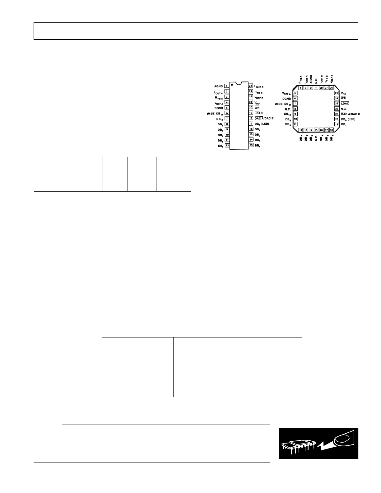
PIN CONNECTIONS
24-Lead 0.3" Cerdip
24-Lead Plastic DIP
24-Lead SOL
28-Terminal LCC
NC = NO CONNECT
ORDERING GUIDE
INL GFSE Temperature Package Package
Model (LSB) (LSB) Range Description Option
DAC8222EW ±1/2 ±1 –40°C to +85°C Cerdip-24 Q-24
DAC8222GP ±1/2 ±20°C to +70°C P-DIP-24 N-24
DAC8222BTC/883* ±1 ± 4 –55°C to +125°C LCC-28 E-28A
DAC8222FW ±1 ± 4 –40°C to +85°C Cerdip-24 Q-24
DAC8222FP ±1 ± 4 –40°C to +85°C P-DIP-24 N-24
DAC8222FS ± 1 ± 4 –40°C to +85°C SOL-24 R-24
*Consult factory for DAC8222/883 MIL-STD data sheet.
CAUTION
ESD (electrostatic discharge) sensitive device. Electrostatic charges as high as 4000 V readily
accumulate on the human body and test equipment and can discharge without detection.
Although the DAC8222 features proprietary ESD protection circuitry, permanent damage may
occur on devices subjected to high energy electrostatic discharges. Therefore, proper ESD
precautions are recommended to avoid performance degradation or loss of functionality.
REV. C
–3–
DAC8222
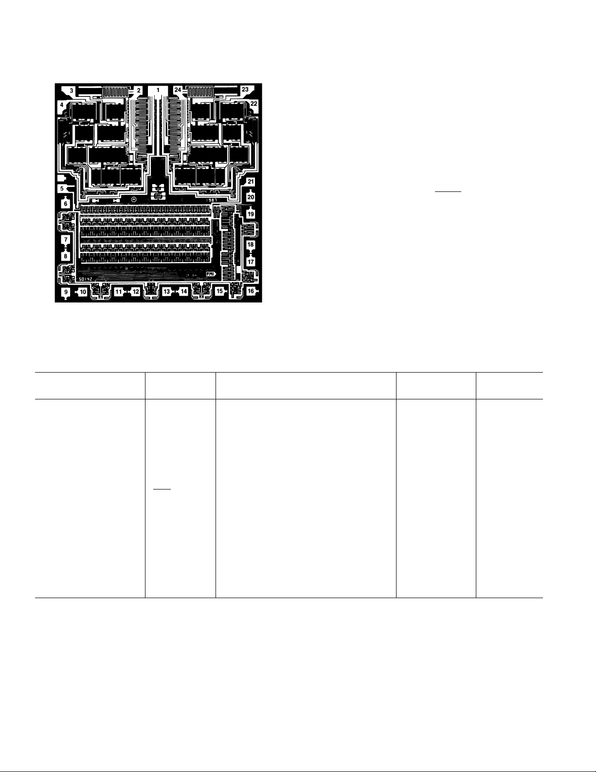
DICE CHARACTERISTICS
DIE SIZE 0.124 × 0.132 inch, 16,368 sq. mils
×
3.55 mm, 10.56 sq. mm)
(3.15
11. AGND 13. DB4
12. I
13. R
14. V
OUT A
FB A
REF A
14. DB3
15. DB2
16. DB1
15. DGND 17. DB0 (LSB)
16. DB11(MSB) 18. DAC A/DAC B
17. DB10 19.
LDAC
18. DB9 20. WR
19. DB8 21. V
10. DB7 22. V
11. DB6 23. R
12. DB5 24. I
DD
REF B
FB B
OUT B
Substrate (die backside) is internally connected to VDD.
WAFER TEST LIMITS
(@ VDD = +5 V or +15 V, V
REF A
= V
= +10 V, V
REF B
OUT A
= V
= 0 V; AGND = DGND = 0 V; TA = +25ⴗC)
OUT B
DAC8222G
Parameter Symbol Conditions Limit Units
Relative Accuracy INL Endpoint Linearity Error ±1LSB max
Differential Nonlinearity DNL All Grades are Guaranteed Monotonic ± 1LSB max
Full Scale Gain Error
1
G
FSE
Digital Inputs = 1111 1111 1111 ±4LSB max
Output Leakage Digital Inputs = 0000 0000 0000 ±50 nA max
(I
, I
OUT A
)I
OUT B
LKG
Pads 2 and 24
Input Resistance
, V
(V
REF A
Input Resistance Match ∆R
Digital Input High V
Digital Input Low V
Digital Input Current I
Supply Current I
)R
REF B
REF
REF
R
REF
INH
INL
IN
DD
DC Supply Rejection PSR ∆V
Pads 4 and 22 8/15 kΩ max
±1% max
VDD = +5 V 2.4 V min
V
= +15 V 13.5 V min
DD
VDD = +5 V 0.8 V max
V
= +15 V 1.5 V min
DD
VIN = 0 V or VDD; V
All Digital Inputs V
All Digital Inputs 0 V or V
= ±5% 0.002 %/% max
DD
INL
INL
or V
or V
DD
INH
INH
±1 µA max
2
0.1 mA max
(∆Gain/∆VDD)
NOTES
1
Measured using internal R
Electrical tests are performed at wafer probe to the limits shown. Due to variations in assembly methods and normal yield loss, yield after packaging is not guaranteed
for standard product dice. Consult factory to negotiate specifications based on dice lot qualification through sample lot assembly and testing.
FB A
and R
FB B
.
–4–
REV. C
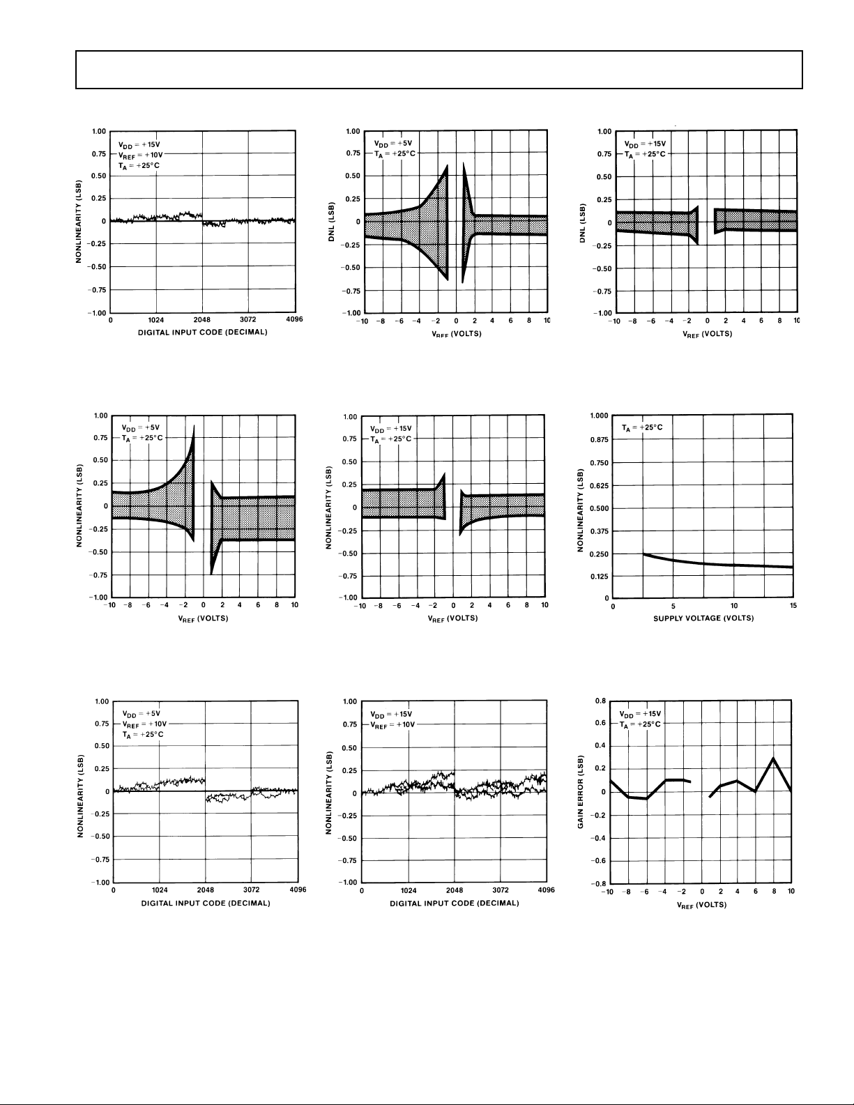
TYPICAL PERFORMANCE CHARACTERISTICS
DAC8222
Figure 1. Channel-to-Channel Matching (DAC A and B are Superimposed)
Figure 4. Nonlinearity vs. V
REF
Figure 2. Differential Nonlinearity
vs. V
REF
Figure 5. Nonlinearity vs. V
REF
Figure 3. Differential Nonlinearity
vs. V
REF
Figure 6. Nonlinearity vs. V
DD
Figure 7. Nonlinearity vs. Code
(DAC A and B are Superimposed)
REV. C
Figure 8. Nonlinearity vs. Code at T
A
= –55°C, +25°C, +125°C for DAC A and
B (All Superimposed)
–5–
Figure 9. Absolute Gain Error
Changes vs. V
REF
 Loading...