3 MSPS,10-/12-Bit
V
FEATURES
Throughput rate: 3 MSPS
Specified for V
Power consumption
11.4 mW at 3 MSPS with 3 V supplies
Wide input bandwidth
70 dB SNR at 1 MHz input frequency
Flexible power/serial clock speed management
No pipeline delays
High speed serial interface
SPI®-/QSPI™-/MICROWIRE™-/DSP-compatible
Temperature range: −40°C to +125°C
Power-down mode: 0.1 μA typ
8-lead TSOT package
8-lead MSOP package
GENERAL DESCRIPTION
The AD7273/AD7274 are 10-/12-bit, high speed, low power,
successive approximation ADCs, respectively. The parts operate
from a single 2.35 V to 3.6 V power supply and feature
throughput rates of up to 3 MSPS. Each part contains a low
noise, wide bandwidth track-and-hold amplifier that can handle
input frequencies in excess of 55 MHz.
The conversion process and data acquisition are controlled
using
with microprocessors or DSPs. The input signal is sampled on
the falling edge of
point. The conversion rate is determined by the SCLK. There
are no pipeline delays associated with these parts.
The AD7273/AD7274 use advanced design techniques to
achieve very low power dissipation at high throughput rates.
The reference for the parts is applied externally and can be in
the range of 1.4 V to V
range to the ADC.
and the serial clock, allowing the devices to interface
CS
of 2.35 V to 3.6 V
DD
, and the conversion is also initiated at this
CS
. This allows the widest dynamic input
DD
ADCs in 8-Lead TSOT
AD7273/AD7274
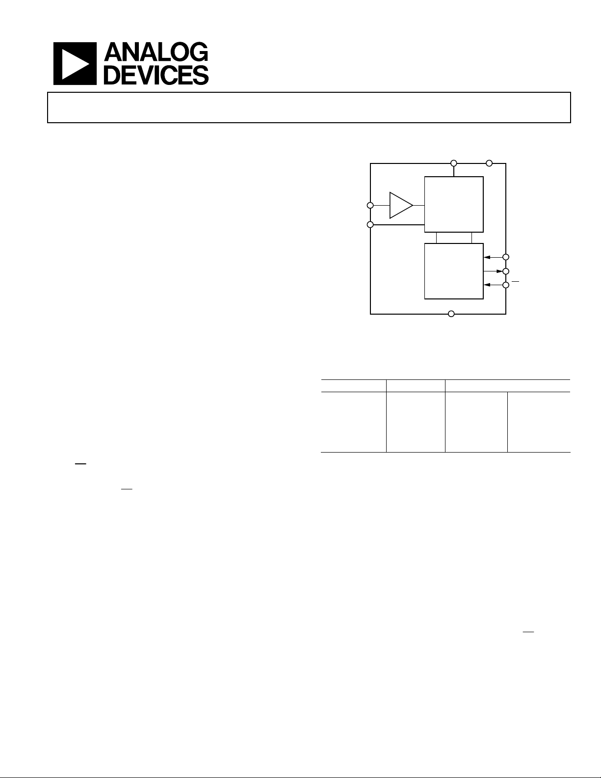
FUNCTIONAL BLOCK DIAGRAM
V
DD
AGND
10-/12-BIT
V
REF
IN
T/H
AD7273/AD7274
Table 1.
Part Number Resolution Package
1
AD7273
AD7274
1
10 8-lead MSOP 8-Lead TSOT
12 8-lead MSOP 8-Lead TSOT
AD7276 12 8-lead MSOP 6-Lead TSOT
AD7277 10 8-lead MSOP 6-Lead TSOT
AD7278 8 8-lead MSOP 6-Lead TSOT
1
Parts contain external reference pin.
PRODUCT HIGHLIGHTS
1. 3 MSPS ADCs in an 8-lead TSOT package.
2. High throughput with low power consumption.
3. Flexible power/serial clock speed management.
Allows maximum power efficiency at low throughput rates.
4. Reference can be driven up to the power supply.
5. No pipeline delay.
SUCCESSIVE
APPROXIMATION
ADC
CONTROL
LOGIC
DGND
Figure 1.
SCLK
SDATA
CS
04973-001
6. The parts feature a standard successive approximation ADC
with accurate control of the sampling instant via a
CS
input
and once-off conversion control.
Rev. 0
Information furnished by Analog Devices is believed to be accurate and reliable. However, no
responsibility is assumed by Anal og Devices for its use, nor for any infringements of patents or ot her
rights of third parties that may result from its use. Specifications subject to change without notice. No
license is granted by implication or otherwise under any patent or patent rights of Analog Devices.
Trademarks and registered trademarks are the property of their respective owners.
One Technology Way, P.O. Box 9106, Norwood, MA 02062-9106, U.S.A.
Tel: 781.329.4700 www.analog.com
Fax: 781.461.3113 © 2005 Analog Devices, Inc. All rights reserved.

AD7273/AD7274
TABLE OF CONTENTS
Features .............................................................................................. 1
ADC Transfer Function............................................................. 15
General Description......................................................................... 1
Functional Block Diagram .............................................................. 1
Product Highlights........................................................................... 1
Revision History ............................................................................... 2
Specifications..................................................................................... 3
AD7274 Specifications................................................................. 3
AD7273 Specifications................................................................. 5
Timing Specifications .................................................................. 7
Timing Examples.......................................................................... 8
Absolute Maximum Ratings............................................................ 9
ESD Caution.................................................................................. 9
Pin Configurations and Function Descriptions .........................10
Typical Performance Characteristics ........................................... 11
Te r mi n ol o g y .................................................................................... 14
Circuit Information........................................................................ 15
Typical C o n ne ction D i a g ram ....................................................... 16
Analog Input............................................................................... 16
Digital Inputs .............................................................................. 16
Modes of Operation ....................................................................... 17
Normal Mode.............................................................................. 17
Partial Power-Down Mode ....................................................... 17
Full Power-Down Mode ............................................................ 17
Power-Up Times ......................................................................... 18
Power vs. Throughput Rate....................................................... 20
Serial Interface................................................................................ 21
Microprocessor Interfacing....................................................... 23
Application Hints ........................................................................... 24
Grounding and Layout .............................................................. 24
Evaluating the AD7273/AD7274 Performance......................... 24
Outline Dimensions ....................................................................... 25
Converter Operation.................................................................. 15
REVISION HISTORY
9/05—Revision 0: Initial Version
Ordering Guide .......................................................................... 25
Rev. 0 | Page 2 of 28

AD7273/AD7274
SPECIFICATIONS
AD7274 SPECIFICATIONS
VDD = 2.35 V to 3.6 V, V
Table 2.
Parameter B Grade
DYNAMIC PERFORMANCE fIN = 1 MHz sine wave
Signal-to-Noise + Distortion (SINAD)
Signal-to-Noise Ratio (SNR) 69.5 dB min
Total Harmonic Distortion (THD)3 −73 dB max
−78 dB typ
Peak Harmonic or Spurious Noise (SFDR)3 −80 dB typ
Intermodulation Distortion (IMD)
Second-Order Terms −82 dB typ fa = 1 MHz, fb = 0.97 MHz
Third-Order Terms −82 dB typ fa = 1 MHz, fb = 0.97 MHz
Aperture Delay 5 ns typ
Aperture Jitter 18 ps typ
Full Power Bandwidth 55 MHz typ @ 3 dB
8 MHz typ @ 0.1 dB
Power Supply Rejection Ratio (PSRR) 82 dB typ
DC ACCURACY
Resolution 12 Bits
Integral Nonlinearity
Differential Nonlinearity
Offset Error
Gain Error
3
3
Total Unadjusted Error (TUE)
ANALOG INPUT
Input Voltage Range 0 to V
DC Leakage Current ±1 μA max −40°C to +85°C
±5.5 μA max 85°C to 125°C
Input Capacitance 42 pF typ When in track
10 pF typ When in hold
REFERENCE INPUT
V
Input Voltage Range 1.4 to V
REF
DC leakage Current ±1 μA max
Input Capacitance 20 pF typ
Input Impedance 32 Ω typ
LOGIC INPUTS
Input High Voltage, V
2 V min 2.7 V < VDD ≤ 3.6 V
Input Low Voltage, V
0.8 V max 2.7 V ≤ VDD ≤ 3.6 V
Input Current, I
IN
Input Capacitance, C
LOGIC OUTPUTS
Output High Voltage, V
Output Low Voltage, V
Floating-State Leakage Current ±2.5 μA max
Floating-State Output Capacitance
Output Coding Straight (natural) binary
= 2.35 V to VDD, f
REF
3
3
3
INH
INL
4
IN
OH
OL
= 48 MHz, f
SCLK
3
68 dB min
= 3 MSPS, TA = T
SAMPLE
1
Unit
to T
MIN
2
, unless otherwise noted.
MAX
Test Conditions/Comments
±1 LSB max
±1 LSB max Guaranteed no missed codes to 12 bits
±3 LSB max
±3.5 LSB max
±3.5 LSB max
REF
DD
V
V min/V max
1.7 V min 2.35 V ≤ VDD ≤ 2.7 V
0.7 V max 2.35 V ≤ VDD < 2.7 V
±1 μA max Typically 10 nA, VIN = 0 V or V
DD
2 pF max
VDD − 0.2 V min I
0.2 V max I
4
4.5 pF max
= 200 μA, VDD = 2.35 V to 3.6 V
SOURCE
= 200 μA
SINK
Rev. 0 | Page 3 of 28
AD7273/AD7274
Parameter B Grade
1
Unit
2
Test Conditions/Comments
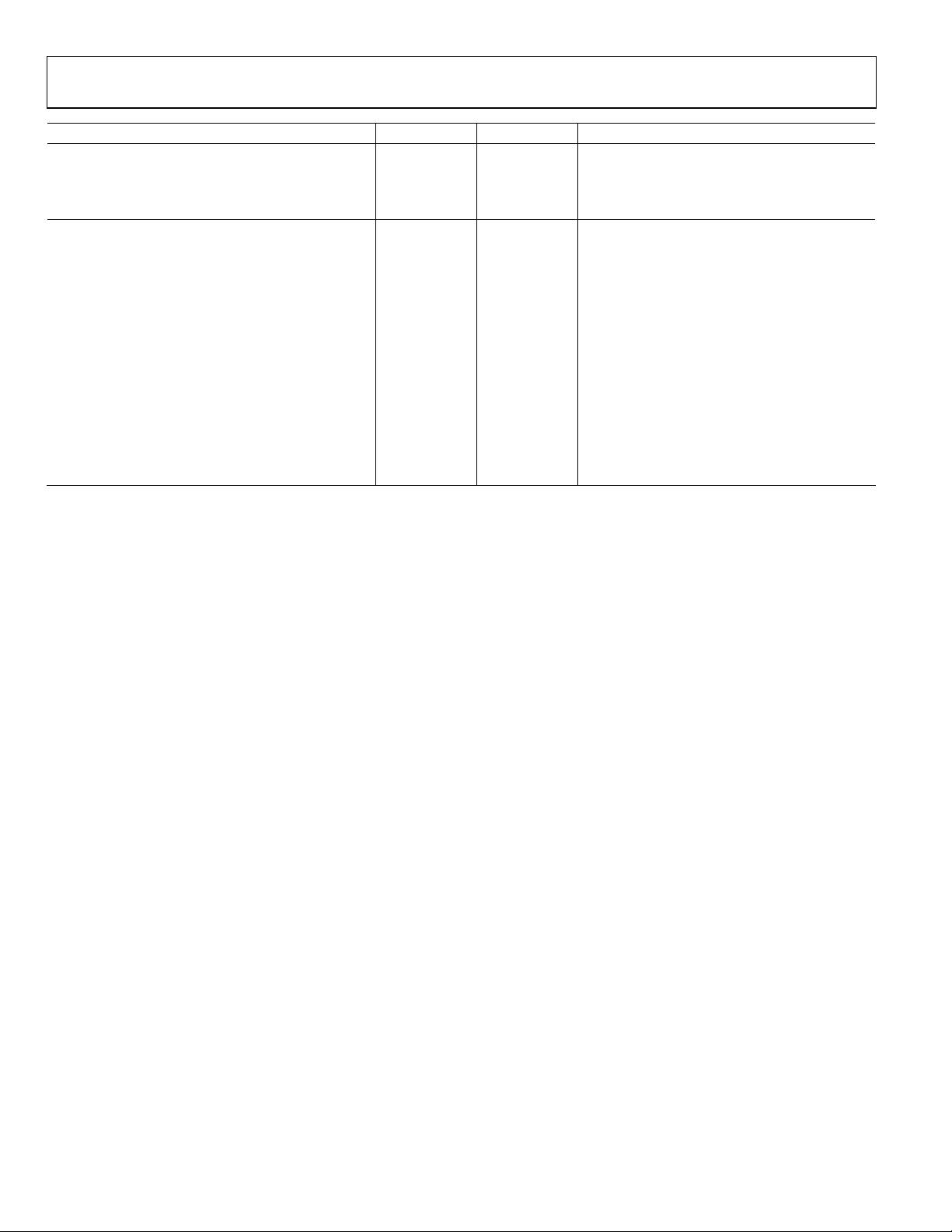
CONVERSION RATE
Conversion Time 291 ns max 14 SCLK cycles with SCLK at 48 MHz
Track-and-Hold Acquisition Time
3
60 ns max
Throughput Rate 3 MSPS max See the Serial Interface section
POWER RQUIREMENTS
V
DD
I
DD
2.35/3.6 V min/V max
Digital I/Ps = 0 V or V
DD
Normal Mode (Static) 1 mA typ VDD = 3 V, SCLK on or off
Normal Mode (Operational) 5 mA max VDD = 2.35 V to 3.6 V, f
SAMPLE
= 3 MSPS
3.8 mA typ VDD = 3 V
Partial Power-Down Mode (Static) 34 μA typ
Full Power-Down Mode (Static) 2 μA max −40°C to +85°C, typically 0.1 μA
10 μA max 85°C to 125°C
Power Dissipation
Normal Mode (Operational) 18 mW max VDD = 3.6 V , f
5
SAMPLE
= 3 MSPS
11.4 mW typ VDD = 3 V
Partial Power-Down 102 μW max VDD = 3 V
Full Power-Down 7.2 μW max VDD = 3.6 V, −40°C to +85°C
1
Temperature range from −40°C to +125°C.
2
Typical specifications are tested with VDD = 3 V and V
3
See the Terminology section.
4
Guaranteed by characterization.
5
See the Power vs. Throughput Rate section.
= 3 V at 25°C.
REF
Rev. 0 | Page 4 of 28

AD7273/AD7274
AD7273 SPECIFICATIONS
VDD = 2.35 V to 3.6 V, V
Table 3.
Parameter B Grade
DYNAMIC PERFORMANCE fIN = 1 MHz sine wave
Signal-to-Noise + Distortion (SINAD)
Total Harmonic Distortion (THD)3 −72 dB max
−77 dB typ
Peak Harmonic or Spurious Noise (SFDR)3 −80 dB typ
Intermodulation Distortion (IMD)
Second-Order Terms −81 dB typ fa = 1 MHz, fb = 0.97 MHz
Third-Order Terms −81 dB typ fa = 1 MHz, fb = 0.97 MHz
Aperture Delay 5 ns typ
Aperture Jitter 18 ps typ
Full Power Bandwidth 74 MHz typ @ 3 dB
10 MHz typ @ 0.1 dB
Power Supply Rejection Ratio (PSRR) 82 dB typ
DC ACCURACY
Resolution 10 Bits
Integral Nonlinearity
Differential Nonlinearity
Offset Error
Gain Error
3
3
Total Unadjusted Error (TUE)
ANALOG INPUT
Input Voltage Range 0 to V
DC Leakage Current ±1 μA max −40°C to +85°C
±5.5 μA max 85°C to 125°C
Input Capacitance 42 pF typ When in track
10 pF typ When in hold
REFERENCE INPUT
V
Input Voltage Range 1.4 to V
REF
DC leakage Current ±1 μA max
Input Capacitance 20 pF typ
Input Impedance 32 Ω typ
LOGIC INPUTS
Input High Voltage, V
2 V min 2.7 V < VDD ≤ 3.6 V
Input Low Voltage, V
0.8 V max 2.7 V ≤ VDD ≤ 3.6 V
Input Current, I
IN
Input Capacitance, C
LOGIC OUTPUTS
Output High Voltage, V
Output Low Voltage, V
Floating-State Leakage Current ±2.5 μA max
Floating-State Output Capacitance
Output Coding Straight (natural) binary
CONVERSION RATE
Conversion Time 250 ns max 12 SCLK cycles with SCLK at 48 MHz
Track-and-Hold Acquisition Time
Throughput Rate 3.45 MSPS max See the Serial Interface section
= 2.35 V to VDD, f
REF
3
3
3
INH
IN
4
IN
OH
OL
3
= 48 MHz, f
SCLK
3
61 dB min
= 3 MSPS, TA = T
SAMPLE
1
Unit
to T
MIN
2
, unless otherwise noted.
MAX
Test Conditions/Comments
±0.5 LSB max
±0.5 LSB max Guaranteed no missed codes to 10 bits
±1 LSB max
±1.5 LSB max
±2.5 LSB max
REF
DD
V
V min/V max
1.7 V min 2.35 V ≤ VDD ≤ 2.7 V
0.7 V max 2.35 V ≤ VDD< 2.7 V
±1 μA max Typically 10 nA, VIN = 0 V or V
DD
2 pF max
VDD − 0.2 V min I
0.2 V max I
4
4.5 pF max
= 200 μA; VDD = 2.35 V to 3.6 V
SOURCE
= 200 μA
SINK
60 ns max
Rev. 0 | Page 5 of 28
AD7273/AD7274
Parameter B Grade
1
Unit
2
Test Conditions/Comments
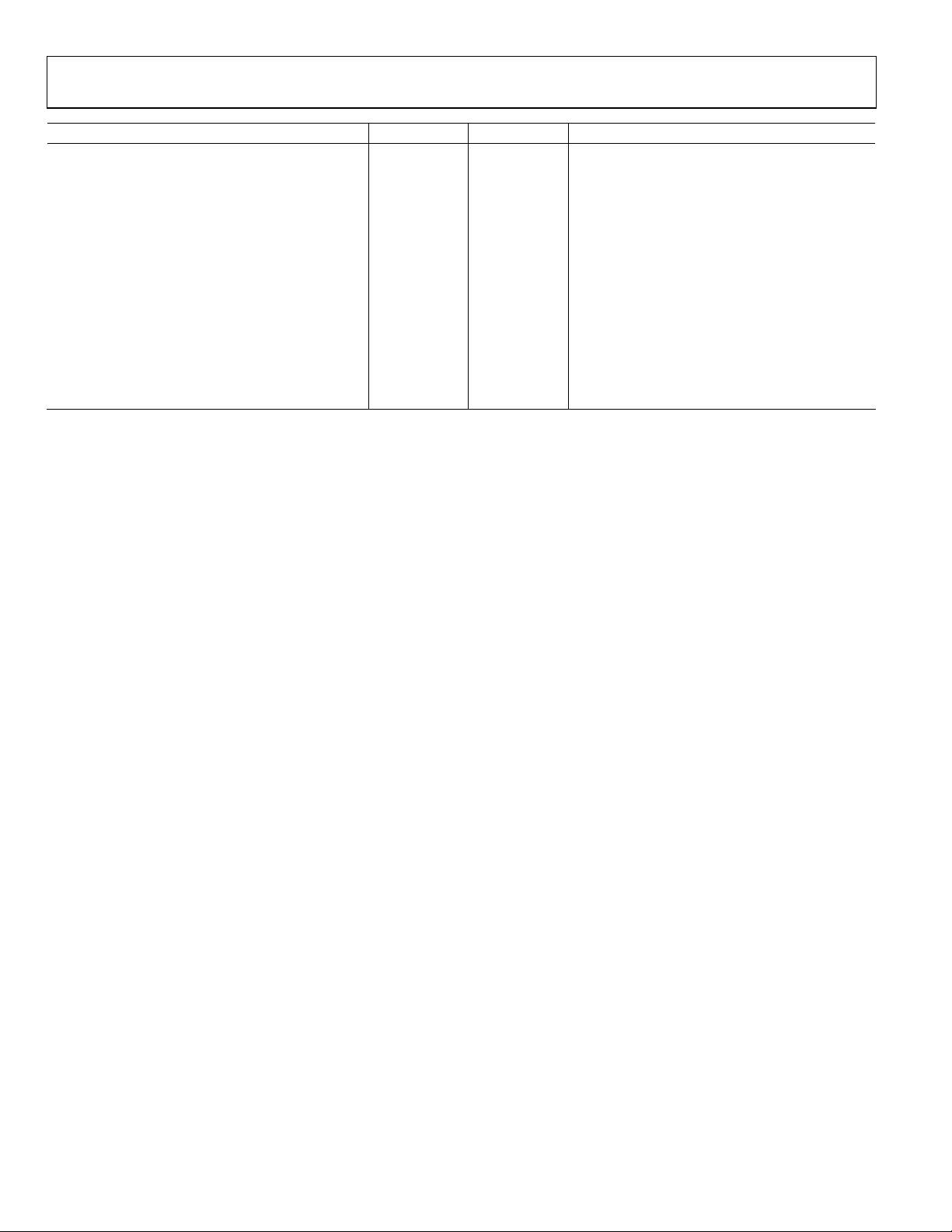
POWER RQUIREMENTS
V
DD
I
DD
2.35/3.6 V min/V max
Digital I/Ps = 0 V or V
Normal Mode (Static) 0.6 mA typ VDD = 3 V, SCLK on or off
Normal Mode (Operational) 5 mA max VDD = 2.35 V to 3.6 V, f
3.2 mA typ V
DD
= 3 V
Partial Power-Down Mode (Static) 34 μA typ
Full Power-Down Mode (Static) 2 μA max −40°C to +85°C, typically 0.1 μA
10 μA max 85°C to 125°C
Power Dissipation
Normal Mode (Operational) 18 mW max VDD = 3.6 V , f
5
SAMPLE
= 3 MSPS
9.6 mW typ VDD = 3 V
Partial Power-Down 102 μW max VDD = 3 V
Full Power-Down 7.2 μW max VDD = 3.6 V, −40°C to +85°C
1
Temperature range from −40°C to +125°C.
2
Typical specifications are tested with VDD = 3 V and V
3
See the Terminology section.
4
Guaranteed by characterization.
5
See the Power vs. Throughput Rate section.
= 3 V at 25°C.
REF
DD
SAMPLE
= 3 MSPS
Rev. 0 | Page 6 of 28
AD7273/AD7274
TIMING SPECIFICATIONS
VDD = 2.35 V to 3.6 V; V
are specified with tr = tf = 2 ns (10% to 90% of V
Table 4.
Limit at T
Parameter
2
f
SCLK
AD7273/AD7274
500 kHz min
48 MHz max
t
CONVER T
14 × t
12 × t
t
QUIET
t
1
t
2
t
3
t
4
t
5
t
6
t
7
t
8
4
4
4
4 ns min
3 ns min
6 ns min
4 ns max
15 ns max Data access time after SCLK falling edge
0.4 t
0.4 t
5 ns min SCLK to data valid hold time
14 ns max SCLK falling edge to SDATA three-state
5 ns min SCLK falling edge to SDATA three-state
t
9
t
POWER-UP
1
Sample tested during initial release to ensure compliance. All timing specifications given are with a 10 pF load capacitance. With a load capacitance greater than this
value, a digital buffer or latch must be used.
2
Mark/space ratio for the SCLK input is 40/60 to 60/40.
3
Minimum f
4
The time required for the output to cross the VIH or VIL voltage.
5
See the Power-Up Times section
4.2 ns max
5
1 μs max Power-up time from full power-down
at which specifications are guaranteed.
SCLK
= 2.35 to VDD; TA = T
REF
, T
MIN
MAX
SCLK
SCLK
SCLK
SCLK
to T
MIN
) and timed from a voltage level of 1.6 V.
DD
, unless otherwise noted.1 Guaranteed by characterization. All input signals
MAX
Unit Description
3
AD7274
AD7273
Minimum quiet time required between bus relinquish and start of
next conversion
Minimum
CS pulse width
CS to SCLK setup time
Delay from
CS until SDATA three-state disabled
ns min SCLK low pulse width
ns min SCLK high pulse width
CS rising edge to SDATA three-state
SCLK
SDATA
SCLK
SDATA
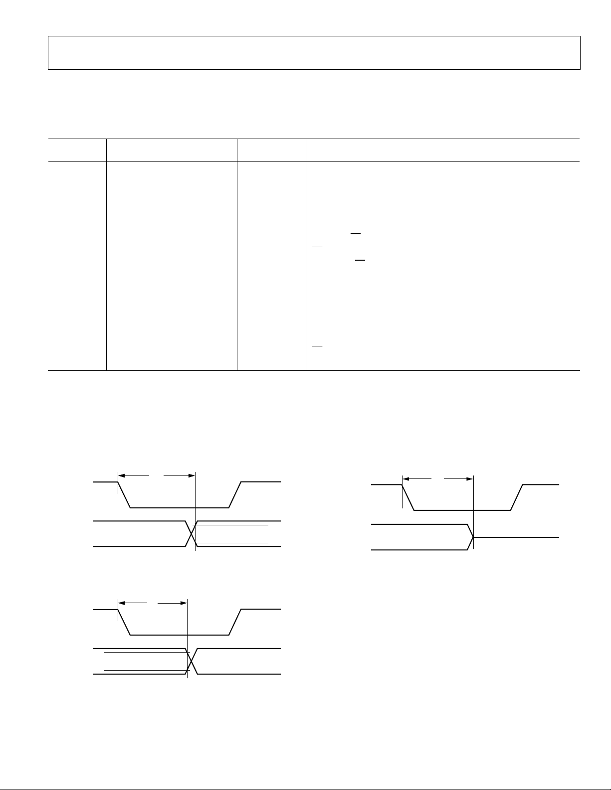
t
4
Figure 2. Access Time After SCLK Falling Edge
t
7
V
IH
V
IL
Figure 3. Hold Time After SCLK Falling Edge
V
IH
V
IL
04973-002
04973-003
Rev. 0 | Page 7 of 28
SCLK
SDATA
t
8
Figure 4. SCLK Falling Edge SDATA Three-State
1.4V
04973-004
AD7273/AD7274
S
A
S
A
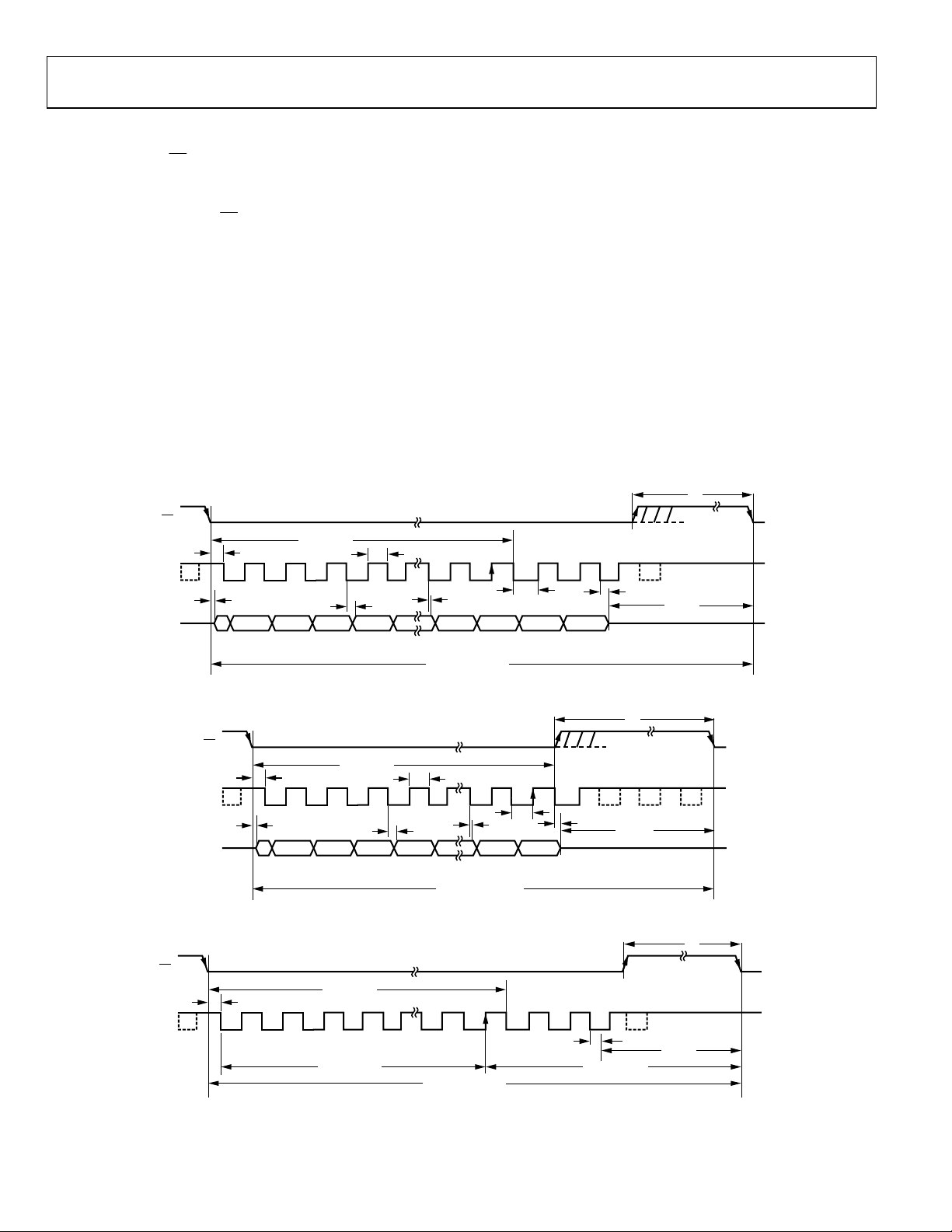
TIMING EXAMPLES
For the AD7274, if CS is brought high during the 14th SCLK
rising edge after the two leading zeros and 12 bits of the
conversion are provided, the part can achieve the fastest
throughput rate, 3 MSPS. If
SCLK rising edge after the two leading zeros, 12 bits of the
conversion, and two trailing zeros are provided, a throughput
rate of 2.97 MSPS is achievable. This is illustrated in the
following two timing examples.
Timing Example 1
In Figure 6, using a 14 SCLK cycle, f
the throughput is 3 MSPS. This produces a cycle time of
t
+ 12.5(1/f
2
t
= 67 ns. This satisfies the requirement of 60 ns for t
ACQ
SCLK
) + t
ACQ
Figure 6 also shows that t
where t
= 4.2 ns max. This allows a value of 52.8 ns for t
9
satisfying the minimum requirement of 4 ns.
CS
SCLK
DAT
STATE
SCLK
DAT
CS
SCLK
is brought high during the 16th
CS
= 48 MHz, and
SCLK
= 333 ns, where t2 = 6 ns min and
ACQ
comprises 0.5(1/f
ACQ
t
2
12345 13141516
t
3
ZEROZ DB11 DB10 DB9 DB1 DB0 ZERO ZERO
TWO LEADING
ZEROS
CS
t
2
12345 1314
t
3
ZEROZ DB11 DB10 DB9 DB1 DB0
TWO LEADING
STATE
t
2
12345 1312 14 15 16
ZEROS
) + t9 + t
SCLK
t
CONVERT
QUIET
QUIET
t
6
t
4
Figure 5. AD7274 Serial Interface Timing 16 SCLK Cycle
t
CONVERT
Figure 6.AD7274 Serial Interface Timing 14 SCLK Cycle
t
CONVERT
12.5(1/f
SCLK
)
Figure 7. Serial Interface Timing 16 SCLK Cycle
.
,
,
t
1/THROUGHPUT
t
6
t
4
1/THROUGHPUT
1/THROUGHPUT
Timing Example 2
The example in Figure 7 uses a 16 SCLK cycle, f
SCLK
and the throughput is 2.97 MSPS. This produces a cycle time
of t
+ 12.5(1/f
2
t
= 70 ns. Figure 7 shows that t
ACQ
t
+ t
8
, where t8 = 14 ns max. This satisfies the minimum
QUIET
requirement of 4 ns for t
B
t
7
5
TWO TRAILING
B
t
5
t
7
B
ZEROS
t
8
SCLK
t
8
t
9
THREE-STATETHREE-
t
ACQUISITION
) + t
= 336 ns, where t2 = 6 ns min and
ACQ
comprises 2.5(1/f
ACQ
QUIET.
t
1
t
QUIET
THREE-STATETHREE-
t
1
t
QUIET
04973-006
t
1
t
QUIET
04973-005
04973-007
= 48 MHz,
SCLK
) +
Rev. 0 | Page 8 of 28
AD7273/AD7274
ABSOLUTE MAXIMUM RATINGS
TA = 25°C, unless otherwise noted.
Table 5.
Parameters Ratings
VDD to AGND/DGND −0.3 V to +6 V
Analog Input Voltage to AGND −0.3 V to VDD + 0.3 V
Digital Input Voltage to DGND −0.3 V to +6 V
Digital Output Voltage to DGND −0.3 V to VDD + 0.3 V
Input Current to Any Pin Except Supplies1±10 mA
Operating Temperature Range
Commercial (B Grade) −40°C to +125°C
Storage Temperature Range −65°C to +150°C
Junction Temperature 150°C
6-Lead TSOT Package
θJA Thermal Impedance 230°C/W
θJC Thermal Impedance 92°C/W
8-Lead MSOP Package
θJA Thermal Impedance 205.9°C/W
θJC Thermal Impedance 43.74°C/W
Lead Temperature Soldering
Reflow (10 to 30 sec) 255°C
Lead Temperature Soldering
Reflow (10 to 30 sec) 260°C
ESD 1.5 kV
1
Transient currents of up to 100 mA cause SCR latch-up.
Stresses above those listed under Absolute Maximum Ratings
may cause permanent damage to the device. This is a stress
rating only; functional operation of the device at these or any
other conditions above those indicated in the operational
section of this specification is not implied. Exposure to absolute
maximum rating conditions for extended periods may affect
device reliability.
ESD CAUTION
ESD (electrostatic discharge) sensitive device. Electrostatic charges as high as 4000 V readily accumulate on
the human body and test equipment and can discharge without detection. Although this product features
proprietary ESD protection circuitry, permanent damage may occur on devices subjected to high energy
electrostatic discharges. Therefore, proper ESD precautions are recommended to avoid performance
degradation or loss of functionality.
Rev. 0 | Page 9 of 28
 Loading...