Analog Devices AD7265 pra Datasheet

Differential Input, Dual 1 MSPS,
Preliminary Technical Data
FEATURES
Dual 12-bit, 3-channel ADC
Fast throughput rate: 1 MSPS
Specified for V
Low power: 7 mW max at 1 MSPS with 3 V supplies
16.5 mW max at 1 MSPS with 5 V supplies
Wide input bandwidth
70 dB SNR at 100 kHz input frequency
On-chip reference: 2.5 V
–40°C to +125°C operation
Flexible power/throughput rate management
Simultaneous conversion/read
No pipeline delays
High speed serial interface SPI®/QSPI™/MICROWIRE™/DSP
compatible
Shutdown mode: 1 µA max
32-lead LFCSP and TQFP packages
GENERAL DESCRIPTION
The AD7265 is a dual, 12-bit, high speed, low power, successive
approximation ADC that operates from a single 2.7 V to 5.25 V
power supply and features throughput rates up to 1 MSPS. The
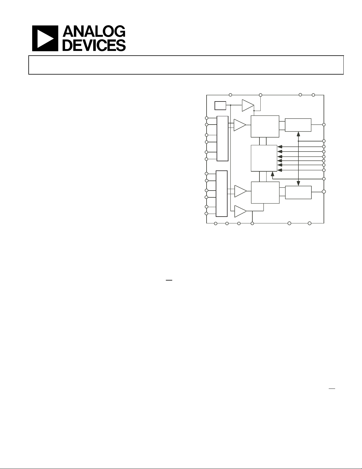
device contains two ADCs, each preceded by a 3-channel multiplexer, and a low noise, wide bandwidth track-and-hold amplifier
that can handle input frequencies in excess of 10 MHz.
The conversion process and data acquisition are controlled using
standard control inputs, allowing easy interfacing to microprocessors or DSPs. The input signal is sampled on the falling edge of
conversion is also initiated at this point. The conversion time is
determined by the SCLK frequency. There are no pipelined delays
associated with the part.
The AD7265 uses advanced design techniques to achieve very low
power dissipation at high throughput rates. With 5 V supplies and a
1 MSPS throughput rate, the part consumes ? mA maximum. The
part also offers flexible power/throughput rate management when
operating in sleep mode.
The analog input range for the part can be selected to be a 0 V to
V
range or a 2V
REF
complement output coding. The AD7265 has an on-chip 2.5 V
reference that can be overdriven if an external reference is preferred. This external reference range is 100 mV to 2.5 V. The
AD7265 is available in 32-lead lead frame chip scale (LFCSP) and
thin flat quad (TQFP) lead package.
Rev. PrA
Information furnished by Analog Devices is believed to be accurate and reliable.
However, no responsibility is assumed by Analog Devices for its use, nor for any
infringements of patents or other rights of third parties that may result from its use.
Specifications subject to change without notice. No license is granted by implication
or otherwise under any patent or patent rights of Analog Devices. Trademarks and
registered trademarks are the property of their respective owners.
of 2.7 V to 5.25 V
DD
range with either straight binary or twos
REF
CS
;
12-Bit, 3-Channel SAR ADC
AD7265
FUNCTIONAL BLOCK DIAGRAM
AD7265
OUTPUT
DRIVERS
OUTPUT
DRIVERS
DGNDAGND
AVdd DVdd
D
REF SELECT
REF
V
A1
V
A2
V
A3
V
A4
V
A5
V
A6
V
B1
V
B2
V
B3
V
B4
V
B5
V
B6
MUX
MUX
AGND DGND
AGND
BUF
T/H
T/H
BUF
A
cap
12-BIT
SUCCESSIVE
APPROXIMATION
ADC
CONTROL
LOGIC
12-BIT
SUCCESSIVE
APPROXIMATION
ADC
D
B
cap
Figure 1
PRODUCT HIGHLIGHTS
1. The AD7265 features two complete ADC functions that allow
simultaneous sampling and conversion of two channels. Each
ADC has 2 analog inputs, 3 fully differential pairs, or 6 singleended channels as programmed. The conversion result of both
channels is available simultaneously on separate data lines, or
in succession on one data line if only one serial port is
available.
2. High Throughput with Low Power Consumption
The AD7265 offers a 1 MSPS throughput rate with ? mW
maximum power consumption when operating at 3 V.
3. Flexible Power/Throughput Rate Management
The conversion rate is determined by the serial clock, allowing
power consumption to be reduced as conversion time is reduced through an SCLK frequency increase. Power efficiency
can be maximized at lower throughput rates if the part enters
sleep between conversions.
4. No Pipeline Delay
The part features two standard successive approximation
ADCs with accurate control of the sampling instant via a
input and once off conversion control.
One Technology Way, P.O. Box 9106, Norwood, MA 02062-9106, U.S.A.
Tel: 781.329.4700 www.analog.com
Fax: 781.326.8703 © 2004 Analog Devices, Inc. All rights reserved.
D
OUT
SCLK
+5
RANGE
DIFF/SE
A0
A1
A2
V
DRIVE
D
OUT
CS
A
B

AD7265 Preliminary Technical Data
TABLE OF CONTENTS
AD7265—Specifications.................................................................. 3
Timing Specifications .................................................................. 4
Absolute Maximum Ratings............................................................ 5
ESD Caution.................................................................................. 5
Pin Configuration and Functional Descriptions.......................... 6
Terminology ...................................................................................... 8
Theory of Operation ...................................................................... 10
Circuit Information.................................................................... 10
Converter Operation.................................................................. 10
Analog Input............................................................................... 11
REVISION HISTORY
Revision PrA: Preliminary Version
Output Coding............................................................................ 11
Transfer Functions ..................................................................... 12
Digital Inputs .............................................................................. 12
V
............................................................................................ 12
DRIVE
Modes of Operation ....................................................................... 13
Normal Mode.............................................................................. 13
Partial Power-Down Mode ....................................................... 13
Full Power-Down Mode............................................................ 14
Outline Dimensions....................................................................... 15
Ordering Guide............................................................................... 16
Rev. PrA | Page 2 of 16

Preliminary Technical Data AD7265
AD7265—SPECIFICATIONS1
Table 1. TA = T
unless otherwise noted
Parameter Specification Unit Test Conditions/Comments
DYNAMIC PERFORMANCE
Signal-to-Noise + Distortion Ratio (SINAD)
Total Harmonic Distortion (THD)
Spurious Free Dynamic Range (SFDR)
Intermodulation Distortion (IMD)
Second Order Terms –88 dB typ
Third Order Terms –88 dB typ
Channel to Channel Isolation –88 dB typ
SAMPLE AND HOLD
Aperture Delay3 10 ns max
Aperture Jitter3 50 ps typ
Aperture Delay Matching3 200 ps max
Full Power Bandwidth 20 MHz typ @ 3 dB
2.5 MHz typ @0.1 dB
DC ACCURACY
Resolution 12 Bits
Integral Nonlinearity
±1.5 LSB max ±0.5 LSB typ; single-ended configuration
Differential Nonlinearity
0 V to V
REF
Offset Error ±3 LSB max
Offset Error Match ±0.5 LSB typ
Gain Error ±2 LSB max
Gain Error Match ±0.6 LSB typ
0 V to 2 × V
Positive Gain Error ±2 LSB max
Zero Code Error ±3 LSB max
Zero Code Error Match ±1 LSB typ
Negative Gain Error ±1 LSB max
ANALOG INPUT
Input Voltage Ranges 0 V to V
0 V to 2 x V
DC Leakage Current ±500 nA max TA = –40°C to +85°C
±1 µA max 85°C < TA ≤ 125°C
Input Capactiance 30 pF typ When in track
10 pF typ When in hold
REFERENCE INPUT/OUTPUT
Reference Output Voltage
Reference Input Voltage Range 0.1/2.5 V min/V max See Typical Performance plots
DC Leakage Current ±30 µA max V
±160 µA max D
Input Capactiance 20 pF typ
V
Output Impedance
REF
Reference Temperature Coefficient 25 ppm/°C max
10 ppm/°C typ
LOGIC INPUTS
Input High Voltage, V
Input Low Voltage, V
Input Current, IIN ±1 µA max Typically 15 nA, VIN = 0 V or V
Input Capacitance, C
MIN
to T
, VDD = 2.7 V to 5.25 V, f
MAX
2
2
2
2
2
= 16 MHz, fS = 1 MSPS, V
SCLK
2
70 dB min fIN = 100 kHz sine wave
= 2.7 V to 5.25 V; Reference = 2.5 V ± 1%,
DRIVE
–75 dB max fIN = 100 kHz sine wave
–76 dB max fIN = 100 kHz sine wave
±1 LSB max ±0.5 LSB typ; differential configuration
±0.95 LSB max Guaranteed no missed codes to 12 bits
Input Range Straight binary output coding
Input Range Twos complement output coding
REF
V
REF
V
REF
4
5
2.8 V min
INH
0.4 V max
INL
3
IN
2.49/2.51 V min/V max
25 Ω typ
10 pF max
RANGE pin low upon
RANGE pin high upon CS falling edge
pin
REF
A, D
CAP
B pins
CAP
CS
falling edge
DRIVE
Rev. PrA | Page 3 of 16

AD7265 Preliminary Technical Data
Parameter Specification Unit Test Conditions/Comments
LOGIC OUTPUTS
Output High Voltage, VOH V
Output Low Voltage, VOL 0.4 V max
Floating State Leakage Current ±1 µA max
Floating State Output Capacitance
3
Output Coding Straight (Natural) Binary
Twos Complement
CONVERSION RATE
Conversion Time 14 SCLK Cycles TBD ns with SCLK = 16 MHz
Track/Hold Acquisition Time
3
Throughput Rate TBD MSPS max
POWER REQUIREMENTS
V
DD
V
2.7/5.25 V min/V max
DRIVE
6
I
DD
Normal Mode (Static) TBD mA max
Operational, fs = 1 MSPS 3.3 mA max VDD = 5 V
2.3 mA max VDD = 3 V
Partial Power-Down Mode TBD mA max fs = 200 kSPS
Partial Power-Down Mode TBD µA max Static
Full Power-Down Mode TBD µA max
Power Dissipation
6
Normal Mode (Operational) 16.5 mW max VDD = 5 V
Partial Power-Down (Static) TBD mW max
Full Power-Down (Static) TBD mW max
NOTES
1
Temperature ranges as follows: -40°C to +125°C
2
See section. Terminology
3
Sample tested during initial release to ensure compliance.
4
Relates to Pins D
5
See Reference section for D
6
See Power Versus Throughput Rate section.
CAP
A or D
B.
CAP
A, D
B output impedances.
CAP
CAP
TIMING SPECIFICATIONS
Table 2. AVDD = DVDD = 2.7 V to 5.25 V, V
Parameter Limit at T
f
SCLK
10 kHz min
20 MHz max
t
CONVERT
14 × t
700 ns max f
t
35 ns max
QUIET
t
2
t
3
t
4
t5 0.4t
t6 0.4t
t
7
t
8
t
9
10 ns min
TBD ns max
TBD ns max Data access time after SCLK falling edge.
SCLK
SCLK
TBD ns min SCLK to data valid hold time
25 ns max
TBD ns min SCLK falling edge to D
TBD ns max SCLK falling edge to D
, T
MIN
MAX
ns max t
SCLK
ns min SCLK high pulse width
DRIVE
Unit Description
ns min SCLK low pulse width
– 0.2 V min
DRIVE
10 pF max
DIFF
SGL/
SGL/
= 1 with 0 V to V
DIFF
= 0; SGL/
DIFF
100 ns max
2.7/5.25 V min/V max
Digital I/Ps = 0 V or V
= 2.7 V to 5.25 V, TA = T
= 1/f
SCLK
SCLK
SCLK
= 20 MHz,
MAX
to T
, unless otherwise noted
MIN
Minimum time between end of serial read and next falling edge of
CS
to SCLK setup time
CS
Delay from
CS
rising edge to D
until D
OUT
A and D
OUT
A, D
B, high impedance
OUT
A, D
OUT
OUT
A, D
OUT
OUT
B are three-state disabled
OUT
B, high impedance
B, high impedance
range selected
REF
= 1 with 0 V to 2 × V
DRIVE
CS
range
REF
Rev. PrA | Page 4 of 16

Preliminary Technical Data AD7265
ABSOLUTE MAXIMUM RATINGS
Table 3. AD7265 Stress Ratings
Parameter Rating
VDD to AGND –0.3 V to +7 V
DVDD to DGND –0.3 V to +7 V
V
to DGND –0.3 V to DVDD
DRIVE
V
to AGND –0.3 V to AVDD
DRIVE
AVDD to DVDD –0.3 V to +0.3 V
AGND to DGND –0.3 V to +0.3 V
Analog Input Voltage to AGND –0.3 V to AVDD +0.3 V
Digital Input Voltage to DGND –0.3 V to +7 V
Digital Output Voltage to GND –0.3 V to V
V
to AGND –0.3 V to AVDD +0.3 V
REF
Input Current to Any Pin Except
Supplies
1
±10 mA
DRIVE
+0.3 V
Operating Temperature Range –40°C to +125°C
Storage Temperature Range –65°C to +150°C
Junction Temperature 150°C
LFCSP Package
θJA Thermal Impedance 108.2°C/W
θJC Thermal Impedance 32.71°C/W
Lead Temperature, Soldering TBD°C/W
Reflow Temperature (10- 30 sec) TBD°C
ESD TBD
1
Transient currents of up to 100 mA will not cause SCR latch up.
Stresses above those listed under Absolute Maximum Ratings
may cause permanent damage to the device. This is a stress
rating only; functional operation of the device at these or any
other conditions above those indicated in the operational
section of this specification is not implied. Exposure to absolute
maximum rating conditions for extended periods may affect
device reliability.
ESD CAUTION
ESD (electrostatic discharge) sensitive device. Electrostatic charges as high as 4000 V readily accumulate on
the human body and test equipment and can discharge without detection. Although this product features
proprietary ESD protection circuitry, permanent damage may occur on devices subjected to high energy
electrostatic discharges. Therefore, proper ESD precautions are recommended to avoid performance
degradation or loss of functionality.
Rev. PrA | Page 5 of 16
 Loading...