Differential/Single-Ended Input, Dual
www.BDTIC.com/ADI
1 MSPS, 12-Bit, 3-Channel SAR ADC
AD7265
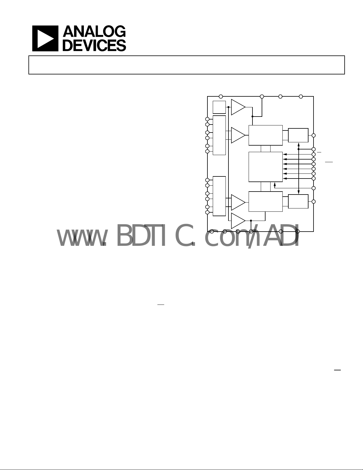
FEATURES FUNCTIONAL BLOCK DIAGRAM
Dual 12-bit, 3-channel ADC
Throughput rate: 1 MSPS
Specified for V
of 2.7 V to 5.25 V
DD
Power consumption
7 mW at 1 MSPS with 3 V supplies
17 mW at 1 MSPS with 5 V supplies
Pin-configurable analog inputs
12-channel single-ended inputs
6-channel fully differential inputs
6-channel pseudo differential inputs
70 dB SINAD at 50 kHz input frequency
Accurate on-chip reference: 2.5 V
±0.2% maximum @ 25°C, 20 ppm/°C maximum
Dual conversion with read 875 ns, 16 MHz SCLK
High speed serial interface
SPI®-/QSPI™-/MICROWIRE™-/DSP-compatible
−40°C to +125°C operation
Shutdown mode: 1 μA maximum
32-lead LFCSP and 32-lead TQFP
2 MSPS version,
AD7266
GENERAL DESCRIPTION
The AD72651 is a dual, 12-bit, high speed, low power, successive
approximation ADC that operates from a single 2.7 V to 5.25 V
power supply and features throughput rates of up to 1 MSPS. The
device contains two ADCs, each preceded by a 3-channel
multiplexer, and a low noise, wide bandwidth track-and-hold
amplifier that can handle input frequencies in excess of 30 MHz.
The conversion process and data acquisition use standard
ntrol inputs allowing easy interfacing to microprocessors or
co
DSPs. The input signal is sampled on the falling edge of
conversion is also initiated at this point. The conversion time is
determined by the SCLK frequency. The AD7265 uses advanced
design techniques to achieve very low power dissipation at high
throughput rates. With 5 V supplies and a 1 MSPS throughput rate,
the part consumes 4 mA maximum. The part also offers flexible
power/throughput rate management when operating in normal
mode, because the quiescent current consumption is so low.
The analog input range for the part can be selected to be a 0 V
to
(or 2 × V
V
REF REF
) range, with either straight binary or twos
complement output coding. The AD7265 has an on-chip 2.5 V
reference that can be overdriven when an external reference is
preferred. This external reference range is 100 mV to V
AD7265 is available in 32-lead LFCSP and 32-lead TQFP.
CS
DD
;
. The
REF SELECT D
BUF
REF
V
A1
V
A2
V
A3
MUX
V
A4
V
A5
V
A6
V
B1
V
B2
V
B3
MUX
V
B4
V
B5
V
B6
AGND AGND AGND D
T/H
T/H
BUF
PRODUCT HIGHLIGHTS
1. Two Complete ADC Functions Allow Simultaneous
Sampling and Conversion of Two Channels.
Each ADC has three fully/pseudo differential pairs, or six
single-ended channels, as programmed. The conversion
result of both channels is simultaneously available on
separate data lines, or in succession on one data line if only
one serial port is available.
2. Hi
gh Throughput with Low Power Consumption.
The AD7265 offers a 1 MSPS throughput rate with 9 mW
maximum power dissipation when operating at 3 V.
3. The AD7265 o
and a 2 × V input range.
4. No Pipeline Delay.
The part features two standard successive approximation
ADCs with accurate control of the sampling instant via a
input and once off conversion control.
1
Protected by U.S. Patent No. 6,681,332.
ffers both a standard 0 V to V
REF
A AV
CAP
12-BIT
SUCCESSIVE
APPROXIMATION
ADC
CONTROL
LOGIC
12-BIT
SUCCESSIVE
APPROXIMATION
ADC
B DGND DGND
CAP
Figure 1.
DD
AD7265
DV
DD
OUTPUT
DRIVERS
OUTPUT
DRIVERS
REF
D
A
OUT
SCLK
CS
RANGE
SGL/DIFF
A0
A1
A2
V
DRIVE
D
B
OUT
input range
CS
04674-001
Rev. A
Information furnished by Analog Devices is believed to be accurate and reliable. However, no
responsibility is assumed by Anal og Devices for its use, nor for any infringements of patents or ot her
rights of third parties that may result from its use. Specifications subject to change without notice. No
license is granted by implication or otherwise under any patent or patent rights of Analog Devices.
Trademarks and registered trademarks are the property of their respective owners.
One Technology Way, P.O. Box 9106, Norwood, MA 02062-9106, U.S.A.
Tel: 781.329.4700 www.analog.com
Fax: 781.461.3113 ©2006 Analog Devices, Inc. All rights reserved.

AD7265
www.BDTIC.com/ADI
TABLE OF CONTENTS
Features .............................................................................................. 1
General Description......................................................................... 1
Functional Block Diagram .............................................................. 1
Product Highlights........................................................................... 1
Revision History ............................................................................... 2
Specifications..................................................................................... 3
Timing Specifications .................................................................. 5
Absolute Maximum Ratings............................................................ 6
ESD Caution.................................................................................. 6
Pin Configurations and Function Descriptions ........................... 7
Typical Performance Characteristics ............................................. 9
Te r mi n ol o g y .................................................................................... 11
Theory of Operation ...................................................................... 13
Circuit Information.................................................................... 13
Converter Operation.................................................................. 13
Analog Input Structure.............................................................. 13
Analog Inputs.............................................................................. 14
Analog Input Selection .............................................................. 17
Output Coding............................................................................ 17
Transf e r Fu ncti o ns ...................................................................... 18
Digital Inputs .............................................................................. 18
V
............................................................................................ 18
DRIVE
Modes of Operation ....................................................................... 19
Normal Mode.............................................................................. 19
Partial Power-Down Mode ....................................................... 19
Full Power-Down Mode ............................................................ 20
Power-Up Times ......................................................................... 21
Power vs. Throughput Rate....................................................... 21
Serial Interface................................................................................ 22
Microprocessor Interfacing ........................................................... 23
AD7265 to ADSP218x............................................................... 23
AD7265 to ADSP-BF53x........................................................... 24
AD7265 to TMS320C541.......................................................... 24
AD7265 to DSP563xx................................................................ 25
Application Hints ........................................................................... 26
Grounding and Layout .............................................................. 26
PCB Design Guidelines for LFCSP.......................................... 26
Evaluating the AD7265 Performance...................................... 26
Outline Dimensions ....................................................................... 27
Ordering Guide .......................................................................... 27
REVISION HISTORY
11/06—Rev. 0 to Rev. A
Changes to Format ............................................................. Universal
Changes to Reference Input/Output Section ................................ 4
Changes to Table 4............................................................................ 7
Changes to Terminology Section.................................................. 11
Changes to Figure 24 and Differential Mode Section................ 15
Changes to Figure 29...................................................................... 16
Changes to AD7265 to ADSP-BF53x Section............................. 24
Updated Outline Dimensions....................................................... 27
Changes to Ordering Guide.......................................................... 27
4/05—Revision 0: Initial Version
Rev. A | Page 2 of 28
AD7265
www.BDTIC.com/ADI
SPECIFICATIONS
TA = T
reference or external reference = 2.5 V ± 1%, unless otherwise noted.
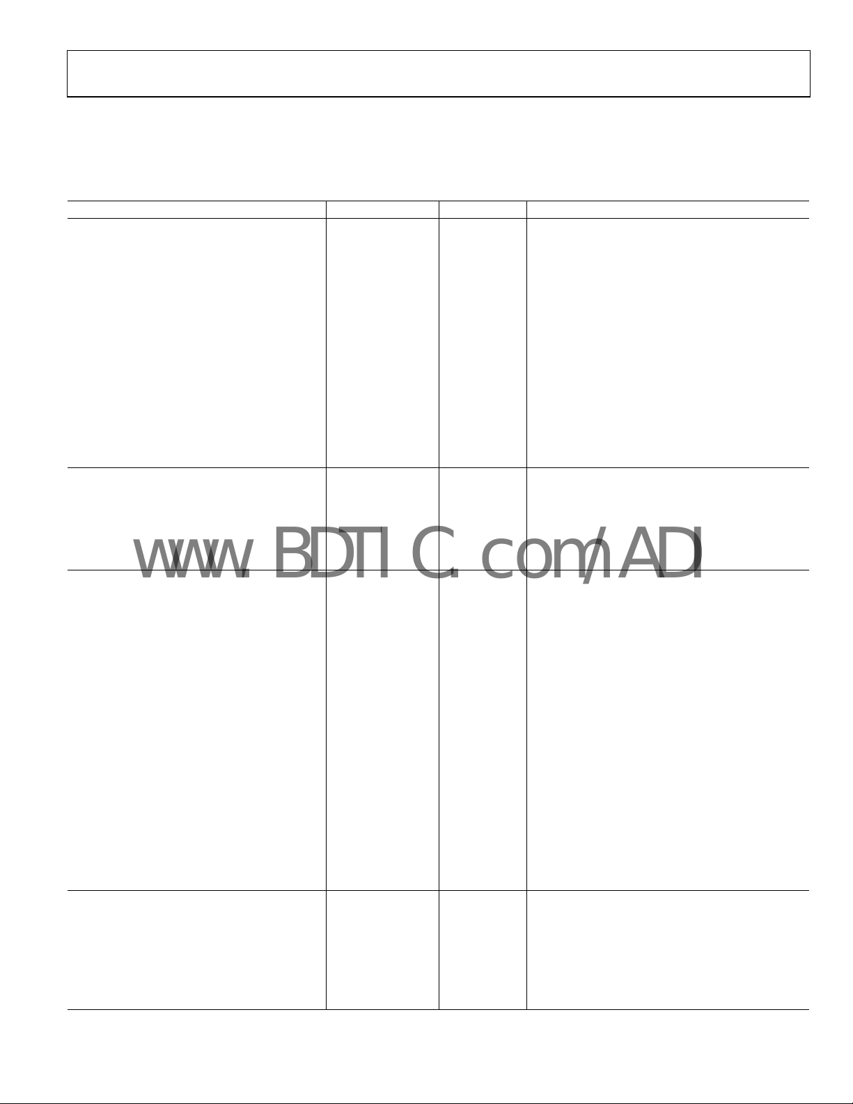
Table 1.
Parameter Specification Unit Test Conditions/Comments
DYNAMIC PERFORMANCE
SAMPLE AND HOLD
3.5/3 MHz typ @ 0.1 dB, VDD = 5 V/VDD = 3 V
DC ACCURACY
±1.5 LSB max
ANALOG INPUTT
to T
MIN
Signal-to-Noise Ratio (SNR)
69 dB min
, VDD = 2.7 V to 5.25 V, f
MAX
2
= 16 MHz, fS = 1 MSPS, V
SCLK
= 2.7 V to 5.25 V; specifications apply using internal
DRIVE
1
71 dB min fIN = 50 kHz sine wave; differential mode
= 50 kHz sine wave; single-ended and
f
IN
pseudo differential modes
Signal-to-Noise + Distortion Ratio (SINAD)270 dB min fIN = 50 kHz sine wave; differential mode
68 dB min
= 50 kHz sine wave; single-ended and
f
IN
pseudo differential modes
Total Harmonic Distortion (THD)
–73 dB max
2
–77 dB max fIN = 50 kHz sine wave; differential mode
= 50 kHz sine wave; single-ended and
f
IN
pseudo differential modes
Spurious-Free Dynamic Range (SFDR)
Intermodulation Distortion (IMD)
2
2
–75 dB max fIN = 50 kHz sine wave
fa = 30 kHz, fb = 50 kHz
Second-Order Terms –88 dB typ
Third-Order Terms
Channel-to-Channel Isolation
Aperture Delay
Aperture Jitter
Aperture Delay Matching
3
3
3
–88 dB typ
–88 dB typ
11 ns max
50 ps typ
200 ps max
Full Power Bandwidth 33/26 MHz typ @ 3 dB, VDD = 5 V/VDD = 3 V
Resolution 12 Bits
Integral Nonlinearity
2
±1 LSB max ±0.5 LSB typ; differential mode
±0.5 LSB typ; single-ended and pseudo
erential modes
diff
Differential Nonlinearity
2,4
±0.99 LSB max Differential mode
−0.99/+1.5 LSB max Single-ended and pseudo differential modes
Straight Binary Output Coding
Offset Error ±6 LSB max
Offset Error Match ±2 LSB typ
Gain Error ±2.5 LSB max
Gain Error Match ±0.5 LSB typ
Twos Complement Output Coding
Positive Gain Error ±2 LSB max
Positive Gain Error Match ±0.5 LSB typ
Zero Code Error ±5 LSB max
Zero Code Error Match ±1 LSB typ
Negative Gain Error ±2 LSB max
Negative Gain Error Match ±0.5 LSB typ
5
Single-Ended Input Range 0 V to V
0 V to 2 × V
Pseudo Differential Input Range: V
IN+
− V
2 × V
Fully Differential Input Range: V
IN+
V
and V
and V
IN+
V RANGE pin low
REF
RANGE pin high
V RANGE pin high
V VCM = V
IN−
IN−
IN−
6
REF
0 to V
V RANGE pin low
REF
REF
VCM ± V
VCM ± V
/2 V VCM = common-mode voltage7 = V
REF
REF
REF
REF
/2
Rev. A | Page 3 of 28

AD7265
www.BDTIC.com/ADI
Parameter Specification Unit Test Conditions/Comments
DC Leakage Current ±1 μA max
Input Capacitance 45 pF typ When in track
10 pF typ When in hold
REFERENCE INPUT/OUTPUT
Reference Output Voltage
Long-Term Stability 150 ppm typ For 1000 hours
Output Voltage Hysteresis
Reference Input Voltage Range 0.1/V
DC Leakage Current ±2 μA max External reference applied to Pin D
Input Capacitance 25 pF typ
D
A, D
CAP
B Output Impedance
CAP
Reference Temperature Coefficient 20 ppm/°C max
10 ppm/°C typ
V
Noise 20 μV rms typ
REF
LOGIC INPUTS
Input High Voltage, V
Input Low Voltage, V
Input Current, I
IN
Input Capacitance, C
LOGIC OUTPUTS
Output High Voltage, V
Output Low Voltage, V
Floating State Leakage Current ±1 μA max
Floating State Output Capacitance
Output Coding
Twos complement
CONVERSION RATE
Conversion Time 14 SCLK cycles 875 ns with SCLK = 16 MHz
Track-and-Hold Acquisition Time
110 ns max Full-scale step input; VDD = 3 V
Throughput Rate 1 MSPS max
POWER REQUIREMENTS
V
DD
V
DRIVE
I
DD
Normal Mode (Static) 2.3 mA max VDD = 5.25 V
Operational, fS = 1 MSPS 4 mA max VDD = 5.25 V; 3.5 mA typ
fS = 1 MSPS 3.2 mA max VDD = 3.6 V; 2.7 mA typ
Partial Power-Down Mode 500 μA max Static
Full Power-Down Mode (VDD) 1 μA max TA = −40°C to +85°C
2.8 μA max TA > 85°C to 125°C
Power Dissipation
Normal Mode (Operational) 21 mW max VDD = 5.25 V
Partial Power-Down (Static) 2.625 mW max VDD = 5.25 V
Full Power-Down (Static) 5.25 μW max VDD = 5.25 V, TA = −40°C to +85°C
1
Temperature range is −40°C to +125°C.
2
See Terminology section.
3
Sample tested during initial release to ensure compliance.
4
Guaranteed no missed codes to 12 bits.
5
V
or V
must remain within GND/VDD.
IN−
IN+
6
V
= 0 V for specified performance. For full input range on V
IN−
7
For full common-mode range, see Figure 24 and Figure 25.
8
Relates to Pin D
A or Pin D
CAP
8
2
INH
INL
3
IN
OH
OL
3
3
2.5 V min/V max ±0.2% max @ 25°C
50 ppm typ
DD
V min/V max See Typical Performance Characteristics section
10 Ω typ
2.8 V min
0.4 V max
±15 nA typ VIN = 0 V or V
DRIVE
5 pF typ
V
− 0.2 V min
DRIVE
0.4 V max
7 pF typ
Straight (natural) binary
SGL/DIFF
SGL/DIFF
= 1 with 0 V to V
range selected
REF
= 0; SGL/DIFF = 1 with 0 V to 2 × V
90 ns max Full-scale step input; VDD = 5 V
A/Pin D
CAP
range
REF
CAP
B
2.7/5.25 V min/V max
2.7/5.25 V min/V max
Digital I/Ps = 0 V or V
DRIVE
pin, see Figure 28 and Figure 29.
IN−
B.
CAP
Rev. A | Page 4 of 28

AD7265
www.BDTIC.com/ADI
TIMING SPECIFICATIONS
AVDD = DVDD = 2.7 V to 5.25 V, V
Table 2.
Parameter Limit at T
2
f
SCLK
1 MHz min TA = −40°C to +85°C
MIN
, T
4 MHz min TA > 85°C to 125°C
16 MHz max
t
CONVER T
14 × t
SCLK
875 ns max f
t
QUIET
t
2
30 ns min
15/20 ns min
20/30 ns min
t
3
3
t
4
15 ns max
36 ns max Data access time after SCLK falling edge, VDD = 3 V
27 ns max Data access time after SCLK falling edge, VDD = 5 V
t
5
t
6
t
7
t
8
t
9
t
10
0.45 t
SCLK
0.45 t
SCLK
10 ns min SCLK to data valid hold time, VDD = 3 V
5 ns min SCLK to data valid hold time, VDD = 5 V
15 ns max
30 ns min
5 ns min SCLK falling edge to D
50 ns max SCLK falling edge to D
1
Sample tested during initial release to ensure compliance. All input signals are specified with tr = tf = 5 ns (10% to 90% of VDD) and timed from a voltage level of 1.6 V.
All timing specifications given are with a 25 pF load capacitance. With a load capacitance greater than this value, a digital buffer or latch must be used. See the Serial
Interface section and Figure 41 and Figure 42.
2
Minimum SCLK for specified performance; with slower SCLK frequencies, performance specifications apply typically.
3
The time required for the output to cross 0.4 V or 2.4 V.
= 2.7 V to 5.25 V, internal/external reference = 2.5 V, TA = T
DRIVE
MAX
Unit Description
ns max t
= 1/f
SCLK
= 16 MHz
SCLK
SCLK
Minimum time between end of serial read and next falling edge of
= 5 V/3 V, CS to SCLK setup time, TA = −40°C to +85°C
V
DD
= 5 V/3 V, CS to SCLK setup time, TA > 85°C to 125°C
V
DD
Delay from CS
until D
ns min SCLK low pulse width
ns min SCLK high pulse width
rising edge to D
CS
rising edge to falling edge pulse width
CS
OUT
A and D
OUT
A, D
B, high impedance
OUT
A, D
OUT
OUT
A, D
OUT
OUT
to T
MAX
B are three-state disabled
OUT
, unless otherwise noted1.
MIN
B, high impedance
B, high impedance
CS
Rev. A | Page 5 of 28
AD7265
www.BDTIC.com/ADI
ABSOLUTE MAXIMUM RATINGS
Table 3.
Parameter Rating
VDD to AGND −0.3 V to +7 V
DVDD to DGND −0.3 V to +7 V
V
to DGND −0.3 V to DV
DRIVE
V
to AGND −0.3 V to AV
DRIVE
AVDD to DV
AGND to DGND −0.3 V to +0.3 V
Analog Input Voltage to AGND −0.3 V to AVDD + 0.3 V
Digital Input Voltage to DGND −0.3 V to +7 V
Digital Output Voltage to GND −0.3 V to V
V
REF
Input Current to Any Pin Except
Supplies
Operating Temperature Range −40°C to +125°C
Storage Temperature Range −65°C to +150°C
Junction Temperature 150°C
LFCSP/TQFP
θJA Thermal Impedance 108.2°C/W (LFCSP)
55°C/W (TQFP)
θJC Thermal Impedance 32.71°C/W (LFCSP)
Lead Temperature, Soldering
Reflow Temperature (10 sec to 30 sec) 255°C
ESD 1.5 kV
1
Transient currents of up to 100 mA will not cause SCR latch up.
DD
to AGND −0.3 V to AVDD + 0.3 V
1
−0.3 V to +0.3 V
±10 mA
DD
DD
DRIVE
+ 0.3 V
Stresses above those listed under Absolute Maximum Ratings
may cause permanent damage to the device. This is a stress
rating only; functional operation of the device at these or any
other conditions above those indicated in the operational
section of this specification is not implied. Exposure to absolute
maximum rating conditions for extended periods may affect
device reliability.
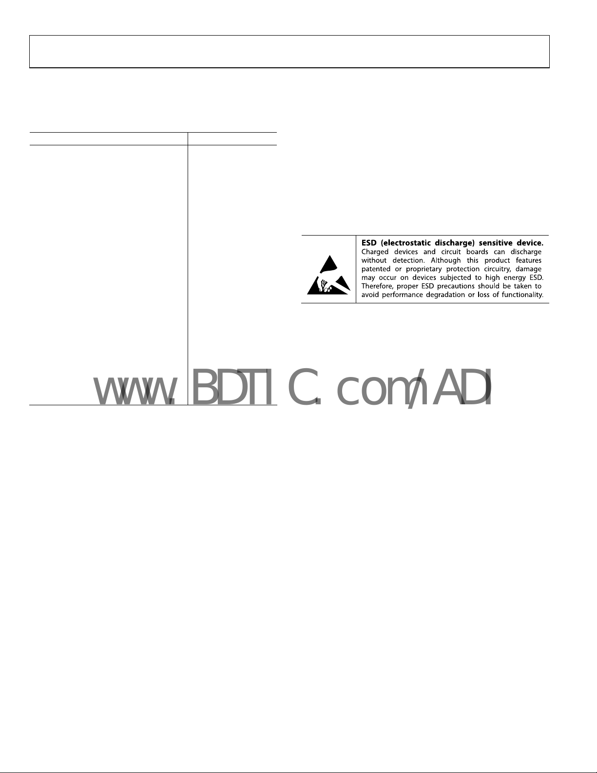
ESD CAUTION
Rev. A | Page 6 of 28
AD7265
www.BDTIC.com/ADI
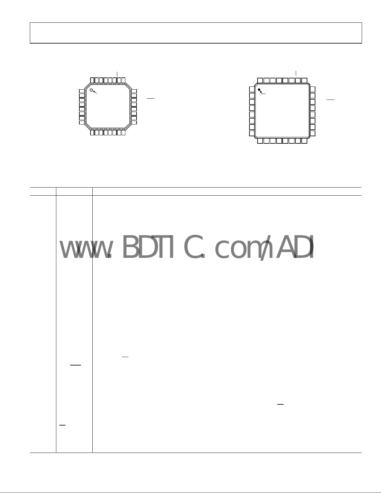
PIN CONFIGURATIONS AND FUNCTION DESCRIPTIONS
A
B
A
DD
OUT
OUT
DRIVE
DGND
D
V
DGND
REF SELECT
AV
D
CAP
AGND
AGND
V
V
DV
32
31302928272625
1
PIN 1
2
INDICATOR
3
DD
4
A
A1
A2
5
6
7
8
AD7265
TOP VIEW
(Not to Scale)
9
101112
A3
D
13
VB6VA6VA5VA4V
CS
SCLK
141516
VB5VB4V
Figure 2. 32-Lead CP-32-2
Table 4. Pin Function Descriptions
Pin No. Mnemonic Description
1, 29 DGND
Digital Ground. This is the ground reference point for all dig
connect to the DGND plane of a system. The DGND and AGND voltages should ideally be at the same potential
and must not be more than 0.3 V apart, even on a transient basis.
2 REF SELECT
Internal/External Reference Selection. Logic input. If this pin is tied to DGND, the on-chip 2.5 V reference is used
as the reference source for both ADC A and ADC B. In addition, Pin D A and Pin D
decoupling capacitors. If the REF SELECT pin is tied to a logic high, an external reference can be supplied to the
AD7265 through the D A pin and/or the D B pin.
3 AV
DD
Analog Supply Voltage, 2.7 V to 5.25 V. This is the only supply voltage for all analog circuitry on the AD7265. The
AV and DV
DD DD
transient basis. This supply should be decoupled to AGND.
4, 20 D A, D B
CAP CAP
Decoupling Capacitor Pins. Decoupling capacitors (470 nF recommended) are connected to these pins to
decouple the reference buffer for each respective ADC. Provided the output is buffered, the on-chip reference
can be taken from these pins and applied externally to the rest of a system. The range of the external reference is
dependent on the analog input range selected.
5, 6, 19 AGND
Analog Ground. Ground reference point for all analog circuitry on the AD7265. All analog input signals and any
external reference signal should be referred to this AGND voltage. All three of these AGND pins should connect
to the AGND plane of a system. The AGND and DGND voltages ideally should be at the same potential and must
not be more than 0.3 V apart, even on a transient basis.
7 to 12 V to V
A1 A6
Analog Inputs of ADC A. These may be programmed as six single-ended channels or three true differential
analog input channel pairs. See Tab le 6.
13 to 18 V
B6
to V
B1
Analog Inputs of ADC B. These may be programmed as six single-ended channels or three true differential
analog input channel pairs. See Tab le 6.
21 RANGE
Analog Input Range Selection. Logic input. The polarity on this pin determines the input range of the analog
input channels. If this pin is tied to a logic low, the analog input range is 0 V to V
high when CS
22
SGL/DIFF
Logic Input. This pin selects whether the analog inputs are configured as differential pairs or single ended. A
logic low selects differential operation while a logic high selects single-ended operation. See the Analog Input
lection section for details.
Se
23 to 25 A2 to A0
Multiplexer Select. Logic inputs. These inputs are used to select the pair of channels to be simultaneously
converted, such as Channel 1 of both ADC A and ADC B, Channel 2 of both ADC A and ADC B, and so on. The pair
of channels selected may be two single-ended channels or two differential pairs. The logic states of these pins
need to be set up prior to the acquisition time and subsequent falling edge of CS
multiplexer for that conversion. See the Analog Input Selection section for further details and Table 6 for
multiplexer address decoding.
26
CS
Chip Select. Active low logic input. This input provides the dual function of initiating conversions on the AD7265
and framing the serial data transfer.
27 SCLK
Serial Clock. Logic input. A serial clock input provides the SCLK f
clock is also used as the clock source for the conversion process.
DD
DV
A0
DGND
REF SELECT
AV
D
CAP
AGND
AGND
V
V
DD
A
A1
A2
B3
24
A1
23
A2
22
SGL/DIFF
21
RANGE
20
D
19
AGND
18
V
17
V
CAP
B1
B2
B
04674-002
V
32
31
1
PIN 1
2
3
4
5
6
7
8
9
10
A3
V
V
Figure 3. 32-Lead SU-32-2
ital circuitry on the AD7265. Both DGND pins should
CAP CAP
CAP CAP
voltages should ideally be at the same potential and must not be more than 0.3 V apart, even on a
goes low, the analog input range is 2 × V . See the Analog Input Selection section for details.
REF
or accessing the data from the AD7265. This
B
OUT
DRIVE
A4
OUT
D
DGND28D
30
29
AD7265
TOP VIEW
(Not to Scale)
11
12
13
A5
A6
B6
V
V
V
CS
SCLK
A0
27
26 25
14
15
16
B5
B4
B3
V
V
V
B must be tied to
. If this pin is tied to a logic
REF
to correctly set up the
24
23
22
21
20
19
18
17
A1
A2
SGL/DIFF
RANGE
D
B
CAP
AGND
V
B1
V
B2
04674-041
Rev. A | Page 7 of 28

AD7265
www.BDTIC.com/ADI
Pin No. Mnemonic Description
28, 30 D
31 V
32 DV
OUT
DRIVE
DD
B, D
A
Serial Data Outputs. The data output is supplied to each pin as a serial da
OUT
the falling edge of the SCLK input and 14 SCLKs are required to access the data. The data simultaneously appears
on both pins from the simultaneous conversions of both ADCs. The data stream consists of two leading zeros
followed by the 12 bits of conversion data. The data is provided MSB first. If
rather than 14, then two trailing zeros appear after the 12 bits of data. If CS is held low for a further 16 SCLK
cycles on either D
simultaneous conversion on both ADCs to be gathered in serial format on either D
serial port. See the Serial Interface section.
Logic Power Supply Input. The voltage supplied at this pin determines at what voltage the interface operates.
This pin should be decoupled to DGND. The voltage at this pin may be different than that at AV
should never exceed either by more than 0.3 V.
Digital Supply Voltage, 2.7 V to 5.25 V. This is the supply voltage for all digital circuitry on the AD7265. The DVDD
and AV
transient basis. This supply should be decoupled to DGND.
voltages should ideally be at the same potential and must not be more than 0.3 V apart even on a
DD
OUT
A or D
B, the data from the other ADC follows on the D
OUT
ta stream. The bits are clocked out on
CS
is held low for 16 SCLK cycles
pin. This allows data from a
OUT
OUT
A or D
B using only one
OUT
DD
and DVDD but
Rev. A | Page 8 of 28
AD7265
www.BDTIC.com/ADI
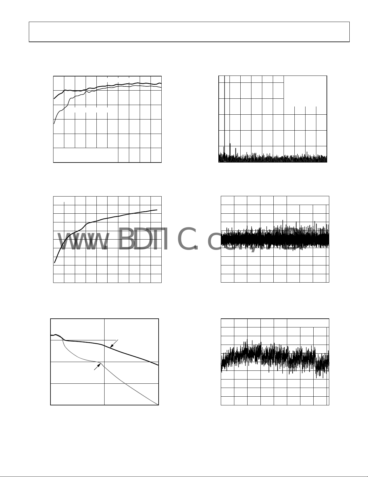
TYPICAL PERFORMANCE CHARACTERISTICS
T = 25°C, unless otherwise noted.
A
–60
–70
–80
–90
PSRR (dB)
–100
INTERNAL REFERENCE
EXTERNAL REFERENCE
–10
–30
–50
(dB)
–70
4096 POINT FFT
V
= 5V, V
DD
F
SAMPLE
F
= 26kHz
IN
SINAD = 71.4dB
THD = –84.42dB
DIFFERENT IAL MODE
DRIVE
= 1MSPS
= 3V
–110
100mV p-p SINE WAVE ON AV
NO DECOUPLING
SINGLE-ENDED MODE
–120
SUPPLY RIPPLE FREQUENCY (kHz)
Figure 4. PSRR vs. Supply Ripple Frequency
DD
20000 200 400 600 800 1000 1200 1400 1600 1800
Without Supply Decoupling
–50
VDD = 5V
–55
–60
–65
–70
–75
–80
ISOLATION (dB)
–85
–90
–95
–100
NOISE FREQUENCY (kHz)
Figure 5. Channel-to-Channe
l Isolation
10000 100 200 300 400 500 600 800700 900
74
72
70
SINAD (dB)
68
66
= 3V
V
DIFFERENTIAL MODE
DD
INPUT FREQUENCY (kHz)
RANGE = 0 TO V
VDD = 5V
DIFFERENTIAL MODE
REF
10000 500
04674-005
Figure 6. SINAD vs. Analog Input Frequency for Various Supply Voltages
04674-003
04674-004
–110
DNL ERROR (LSB)
INL ERROR (LSB)
–90
1.0
0.8
0.6
0.4
0.2
–0.2
–0.4
–0.6
–0.8
–1.0
1.0
0.8
0.6
0.4
0.2
–0.2
–0.4
–0.6
–0.8
–1.0
FREQUENC Y (kHz)
5000 50 100 150 200 250 300 350 400 450
04674-006
Figure 7. FFT
VDD = 5V, V
DIFFERENTIAL MODE
0
CODE
DRIVE
= 3V
40000 1000 2000 3000 3500500 1500 2500
04674-007
Figure 8. Typical DNL
VDD = 5V, V
DIFFERENTIAL MODE
0
CODE
DRIVE
= 3V
40000 500 1000 1500 2000 2500 3000 3500
04674-008
Figure 9. Typical INL
Rev. A | Page 9 of 28
 Loading...