

Page 1
LC2MOS
a
FEATURES
Single +5 V Supply
Transmit Channel
On-Chip GMSK Modulator
Two 10-Bit D/A Converters
Analog Reconstruction Filters
Power-Down Mode
Receive Channel
Two Sigma-Delta A/D Converters
FIR Digital Filters
On-Chip Offset Calibration
Power-Down Mode
3 Auxiliary D/A Converters
Power-Down Modes
On-Chip Voltage Reference
Low Power
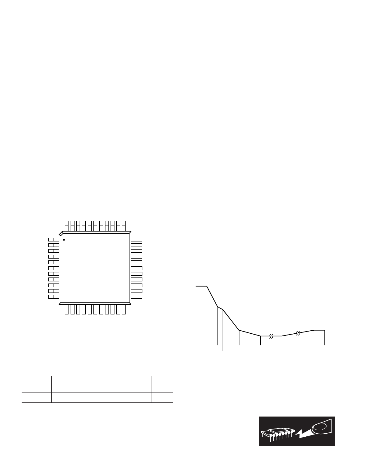
44-Lead PQFP
APPLICATIONS
GSM
PCN
GSM Baseband I/O Port
AD7002
GENERAL DESCRIPTION
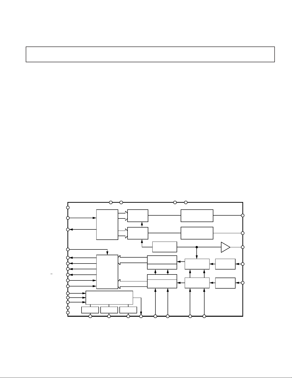
The AD7002 is a complete low power, two-channel, input/
output port with signal conditioning. The device is used as a
baseband digitization subsystem, performing signal conversion
between the DSP and the IF/RF sections in the Pan-European
telephone system (GSM).
The transmit path consists of an onboard digital modulator,
containing all the code necessary for performing Gaussian Minimum Shift Keying (GMSK), two high accuracy, fast DACs with
output reconstruction filters. The receive path is composed of
two high performance sigma-delta ADCs with digital filtering. A
common bandgap reference feeds the ADCs and signal DACs.
Three control DACs (AUX DAC1 to AUX DAC3) are included for such functions as AFC, AGC and carrier signal shaping. In addition, AUX FLAG may be used for routing digital
control information through the device to the IF/RF sections.
As it is a necessity for all GSM mobile systems to use the lowest
power possible, the device has power-down or sleep options for
all sections (transmit, receive and auxiliary).
The AD7002 is housed in 44-lead PQFP (Plastic Quad Flatpack).
Tx SLEEP
Tx DATA
Tx CLK
THREE-STATE
ENABLE
Rx CLK
Rx DATA (I DATA)
Rx SYNC
I/Q (Q DATA)
RATE
MODE
AUX DATA
AUX CLK
AUX LATCH
Rx SLEEP1
Rx SLEEP2
FUNCTIONAL BLOCK DIAGRAM
DV
DGND
DD
10-BIT DAC
GMSK PULSE
SHAPING ROM
10-BIT DAC
RECEIVE
CHANNEL
SERIAL
INTERFACE
16-BIT SHIFT REGISTER
9-BIT DAC 10-BIT DAC 8-BIT DAC
AUX
DAC 1
AUX
DAC 2
AUX
DAC 3
AUX
FLAG
2.5V
REFERENCE
I CHANNEL
DIGITAL FIR FILTER
OFFSET REGISTER
OFFSET REGISTER
Q CHANNEL
DIGITAL FIR FILTER
CAL
CLK2
AV
DD
AGND
4TH ORDER BESSEL
LOW-PASS FILTER
4TH ORDER BESSEL
LOW-PASS FILTER
Σ−∆ MODULATOR
Σ−∆ MODULATOR
CLK1 MZERO
AD7002
REFERENCE
OUTPUT BUFFER
SWITCH-CAP
FILTER
SWITCH-CAP
FILTER
I Tx
Q Tx
REF OUT
I Rx
Q Rx
REV. B
Information furnished by Analog Devices is believed to be accurate and
reliable. However, no responsibility is assumed by Analog Devices for its
use, nor for any infringements of patents or other rights of third parties
which may result from its use. No license is granted by implication or
otherwise under any patent or patent rights of Analog Devices.
One Technology Way, P.O. Box 9106, Norwood, MA 02062-9106, U.S.A.
Tel: 617/329-4700 World Wide Web Site: http://www.analog.com
Fax: 617/326-8703 © Analog Devices, Inc., 1997
Page 2

AD7002–SPECIFICATIONS
(AVDD = +5 V 6 10%; DVDD = +5 V 6 10%; AGND = DGND = 0 V, f
1
TA = T
MIN
to T
, Rx SLEEP1 = Rx SLEEP2 = Tx SLEEP = DVDD, unless otherwise noted)
MAX
CLK1
= f
= 13 MHz;
CLK2
Parameter AD7002A Units Test Conditions/Comments
ADC SPECIFICATIONS
Resolution 12 Bits Rx SLEEP = 0 V, Tx SLEEP = V
Signal Input Span ±V
/2 Volts Biased on V
REF
(2.5 V)
REF
DD
Sampling Rate 13 MSPS
Output Word Rate 270.8 kHz RATE 0
541.7 kHz RATE 1
Accuracy
Integral ±1 LSB typ
Differential
2
0
Bias Offset Error ±6.5 LSB max After External Calibration; MZERO Low
±8 LSB typ After Internal Calibration; MZERO High
Input Resistance (DC) 300 kΩ typ
Input Capacitance 10 pF typ
Dynamic Specifications Input Frequency = 67.7 kHz
Dynamic Range 64 dB typ
Signal to (Noise+Distortion) 62 dB min
Gain Error ±0.5 dB max Input Frequency = 67.7 kHz, w.r.t. 2.5 V
Gain Match Between Channels ±0.15 dB max Input Frequency = 67.7 kHz
Filter Settling Time 47 µs typ
Frequency Response
0 kHz–100 kHz ±0.05 dB max
110 kHz –0.8 dB max
122 kHz –3.0 dB max
200 kHz –66 dB max
400 kHz–6.5 MHz –72 dB max
Absolute Group Delay 23 µs typ
Group Delay Between Channels (0 kHz–120 kHz) 5 ns typ
Coding Twos Complement
Power-Down Option Yes Rx SLEEP = VDD, Independent of Transmit
TRANSMIT DAC SPECIFICATIONS
Resolution 10 Bits Rx SLEEP = V
, Tx SLEEP = 0 V
DD
Number of Channels 2
Update Rate 4.33 MSPS 163 Oversampling of the Bit Rate
DC Accuracy
Integral ±0.7 LSB typ
Differential ±1.0 LSB typ
Output Signal Span ±V
/2 Volts Centered on V
REF
Nominal (100 kΩ/20 pF
REF
Load)
Output Signal Full-Scale Accuracy ±1 dB max w.r.t. 2.5 V
Offset Error ±25 mV max 10 0000 0000 Loaded to DAC
I Tx & Q Tx Gain Matching ±0.15 dB max
Absolute Group Delay 10 µs typ Measured at 67.7 kHz
Group Delay Linearity (0 kHz–120 kHz) 30 ns typ Each Channel, 10 kHz < F
Phase Matching Between Channels 0.5 ° typ Generating 67.7 kHz Sine Waves
GMSK Spectrum Mask
3
< 100 kHz
OUT
100 kHz –3 dB min
200 kHz –32 dB min
250 kHz –35 dB min
400 kHz –63 dB min
0.6 MHz –71 dB min
4.3 MHz –63 dB min
6.5 MHz –63 dB min
GMSK Phase Trajectory Error
Maximum Phase Effect Instance
3
3
2 ° rms max
6 ° peak max
9 µs typ
Output Impedance
I Tx 120 Ω typ
Q Tx 120 Ω typ
GMSK ROM Yes Contains GMSK Coding, Four-Bit Impulse
Response
Power-Down Option Yes Tx SLEEP = VDD, Independent of Receive
–2–
REV. B
Page 3

AD7002
Parameter AD7002A Units Test Conditions/Comments
AUXILIARY DAC SPECIFICATIONS AUX1 AUX2 AUX3
Resolution 9 10 8 Bits
DC Accuracy
Integral ±2 ±2 ± 1 LSB max
Differential ±1 ±1 ±1 LSB max Guaranteed Monotonic
Offset Error ±2 ±4 ±1 LSB max
Gain Error ±4 ±4 ±2 LSB max
LSB Size 4.88 2.44 9.77 mV typ
Output Signal Span 0 to V
REF
0 to V
Output Impedance 10 10 10 kΩ max AUX DACs Have Unbuffered
888 kΩ typ
Coding Binary Binary Binary
Power-Down Yes Yes Yes Power-Down Is Implemented by
REFERENCE SPECIFICATIONS
REFOUT, Reference Output 2.4/2.6 V min/V max R
REFOUT, Reference Output @ +25°C 2.5 V typ R
Reference Temperature Coefficient 100 ppm/°C typ
Reference Variation
4
± 10 mV max
Output Impedance 60 Ω typ
LOGIC INPUTS
, Input High Voltage VDD – 0 9 V min
V
INH
, Input Low Voltage 0.9 V max
V
INL
, Input Current 10 µA max
I
INH
CIN, Input Capacitance 10 pF max
LOGIC OUTPUTS
, Output High Voltage 4.0 V min |I
V
OH
VOL, Output Low Voltage 0.4 V max |I
POWER SUPPLIES
AV
DD
DV
DD
I
DD
All Sections Active 30 mA max
ADC and Auxiliary Paths Active
Transmit DAC and AUX Paths Active
Auxiliary Path only Active
NOTES
1
Operating temperature range: A Version: –40°C to +85°C.
2
Unmeasurable: sigma-delta conversion is inherently free of differential nonlinearities.
3
See terminology.
4
Change in reference voltage due to a change in Tx SLEEP or Rx SLEEP modes.
5
Measured while the digital inputs to the transmit interface are static.
6
Measured while the digital inputs to the receive interface are static.
7
Measured while the digital inputs to the auxiliary interface are static.
Specifications subject to change without notice.
5
6
5, 6, 7
4.5/5.5 V min/V max
4.5/5.5 V min/V max
18 mA max Tx SLEEP = V
15 mA typ
14 mA max Rx SLEEP1 = Rx SLEEP2 = V
11 mA typ
2 mA max Tx SLEEP = Rx SLEEP1 =
REF
0 to V
Volts Unloaded Output
REF
Resistive Outputs
Loading All 1s or All 0s
= 100 kΩ, C
L
= 100 kΩ, C
L
| ≤ 200 µA
OUT
| ≤ 1.6 mA
OUT
Rx SLEEP2 = V
= 1 nF
L
= 1 nF
L
DD
DD
DD
–3–REV. B
Page 4
AD7002
WARNING!
ESD SENSITIVE DEVICE
ABSOLUTE MAXIMUM RATINGS
(T
= +25°C unless otherwise noted)
A
1
DVDD to AGND . . . . . . . . . . . . . . . . . . . . . . . –0.3 V to +7 V
AV
to AGND . . . . . . . . . . . . . . . . . . . . . . . –0.3 V to +7 V
DD
AGND to DGND . . . . . . . . . . . . . . . . . . . . –0.3 V to +0.3 V
Digital Input Voltage to DGND . . . . –0.3 V to DV
Analog Input Voltage to AGND . . . . –0.3 V to AV
Input Current to Any Pin Except Supplies
2
. . . . . . . . ±10 mA
+ 0.3 V
DD
+ 0.3 V
DD
Operating Temperature Range
Industrial Plastic (A Version) . . . . . . . . . . . –40°C to +85°C
Storage Temperature Range . . . . . . . . . . . –65°C to +150°C
Lead Temperature (Soldering, 10 secs) . . . . . . . . . +300°C
Power Dissipation (Any Package) to +75°C . . . . . . . 450 mW
Derates Above +75°C by . . . . . . . . . . . . . . . . . . . . 10 mW/°C
NOTES
1
Stresses above those listed under Absolute Maximum Ratings may cause permanent damage to the device. This is a stress rating only; functional operation of the
device at those or any other conditions above those listed in the operational sections
of this specifications is not implied. Exposure to absolute maximum rating
conditions for extended periods may affect device reliability.
2
Transient currents of up to 100 mA will not cause SCR latch-up.
PIN DESCRIPTION
DD
AUX DAC2
Q Tx
AV
AGND
38
37
39
36
17
18
20
19
NC
Rx SYNC
I/Q (QDATA)
Rx DATA (IDATA)
AUX DAC3
AUX DAC1
35
34
22
21
Rx CLK
3-STATE ENABLE
33
AUX FLAG
32
AUX LATCH
31
AUX CLK
AUX DATA
30
MZERO
29
28
NC
Rx SLEEP1
27
26
TEST2
25
NC
24
Rx SLEEP2
23
CAL
Tx SLEEP
Tx DATA
Tx CLK
DV
DGND
NC
CLK1
TEST1
NC
NC
CLK2
DD
I Rx
44
1
2
3
4
5
6
7
8
9
10
11
NC = NO CONNECT
PIN 1 IDENTIFIER
12
RATE
TEST4
REFOUT
I Tx
Q Rx
42
40
43
41
AD7002 PQFP
TOP VIEW
(Not to Scale)
13
15
14
16
DD
DV
DGND
MODE
TEST3
TERMINOLOGY
Absolute Group Delay
Absolute group delay is the rate of change of phase versus fre-
quency, dθ/df. It is expressed in microseconds.
Bias Offset Error
This is the offset error (in LSBs) in the ADC section.
Differential Nonlinearity
This is the difference between the measured and the ideal
1 LSB change between any two adjacent codes in the DAC
or ADC.
Dynamic Range
Dynamic Range is the ratio of the maximum output signal to the
smallest output signal the converter can produce (1 LSB), expressed logarithmically, in decibels (dB = 20log
an N-bit converter, the ratio is theoretically very nearly equal to
N
2
(in dB, 20Nlog10(2) = 6.02N). However, this theoretical
(ratio)). For
10
value is degraded by converter noise and inaccuracies in the
LSB weight.
Full-Scale Accuracy
This is the measure of the ADC full-scale error after the offset
has been adjusted out.
Gain Error
This is a measure of the output error between an ideal DAC and
the actual device output with all ls loaded after offset error has
been adjusted out and is expressed in LSBs. In the AD7002,
gain error is specified for the auxiliary section.
Gain Matching Between Channels
This is the gain matching between the ITx and QTx channel
and is expressed in dBs.
GMSK Spectrum Mask
This is the combined output spectrum of the I and Q analog
outputs when transmitting a random sequence of data bits on
the AD7002 transmit channel.
–3
–32
–35
AMPLITUDE – dB
100 200
250
–63
–71 –71
400 600 1800 4300
FREQUENCY – kHz
–63
–63
6500
ORDERING GUIDE
AD7002 Transmit GMSK Spectrum Mask
Temperature Package Package
Model Range Description Option
AD7002AS –40°C to +85°C Plastic Quad Flatpack S-44
CAUTION
ESD (electrostatic discharge) sensitive device. Electrostatic charges as high as 4000 V readily
accumulate on the human body and test equipment and can discharge without detection.
Although the AD7002 features proprietary ESD protection circuitry, permanent damage may
occur on devices subjected to high energy electrostatic discharges. Therefore, proper ESD
precautions are recommended to avoid performance degradation or loss of functionality.
–4–
REV. B
Page 5
AD7002
GMSK Phase Trajectory Error
This is a measure of the phase error between the transmitted
phase of an ideal GMSK modulator and the actual phase trans-
mitted by the AD7002, when transmitting a random sequence
of data bits. It is specified as a peak phase error and also as an
rms phase error.
Group Delay Linearity
The group delay linearity, or differential group delay, is the
group delay over the full band relative to the group delay at one
particular frequency. The reference frequency for the AD7002 is
1 kHz.
Group Delay Between Channels
This is the difference between the group delay of the I and Q
channels and is a measure of the phase matching characteristics
of the two.
Integral Nonlinearity
This is the maximum deviation from a straight line passing
through the endpoints of the DAC or ADC transfer function.
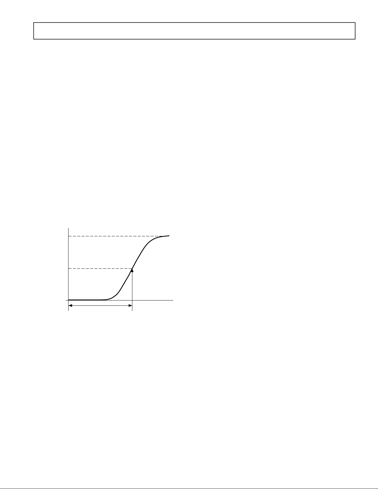
Maximum Phase Effect Instance
This is the time at which a transmitted data bit will have its
maximum phase change at the ITx and QTx outputs (see fig-
ure). This time includes the delay in the GMSK modulator and
in the Analog low-pass filters. Maximum phase effect instance is
measured from the Tx CLK falling edge, which latches the data
bit, to the ITx and QTx analog outputs.
90
°
45
°
FOR ONE DATA BIT
TRANSMITTED PHASE
0
°
≈ 9µs
DATA BIT
CLOCKED IN BY TxCLK
MAXIMUM PHASE
EFFECT INSTANT
Transmit Channel Maximum Phase Effect Instance
Output Rate
This is the rate at which data words are made available at the
Rx DATA pin (Mode 0) or the IDATA and QDATA pins
(Mode 1). There are two rates, depending on whether the de-
vice is operated in RATE0 or RATE1.
Offset Error
This is the amount of offset, w.r.t. V
in the transmit DACs
REF
and the auxiliary DACs and is expressed in mVs for the Transmit section and in LSBs for the Auxiliary section.
Output Impedance
This is a measure of the drive capability of the auxiliary DAC
outputs and is expressed in kΩs.
Output Signal Span
This is the output signal range for the Transmit Channel section
and the Auxiliary DAC section. For the transmit channel the
span is ±1.25 volts centered on 2.5 volts, and for the Auxiliary
DAC section it is 0 to +V
REF
.
Output Signal Full-Scale Accuracy
This is the accuracy of the full-scale output (all 1s loaded to the
DACs) on each transmit channel measured w.r.t. 25 V and is
expressed in dBs.
Phase Matching Between Channels
This is a measure of the phase matching characteristics of the I
and Q transmit channels. It is obtained by transmitting all ones
and then measuring the difference between the actual phase
shift between the I and Q outputs and the ideal phase shift of
90°.
Sampling Rate
This is the rate at which the modulators on the receive channels
sample the analog input.
Settling Time
This is the digital filter settling time in the AD7002 receive
section. On initial power-up, or after returning from the sleep
mode, it is necessary to wait this amount of time to obtain useful data.
Signal Input Span
The input signal range for the I and Q channels is biased about
V
. It can go ±1.25 volts about this point.
REF
Signal to (Noise + Distortion) Ratio
This is the measured ratio of signal-to-(noise + distortion) at the
output of the receive channel. The signal is the rms amplitude of
the fundamental. Noise is the rms sum of all amplitude of the
fundamental. Noise is the rms sum of all nonfundamental signals up to half the sampling frequency (f
/2), excluding dc. The
S
ratio is dependent upon the number of quantization levels in the
digitization process; the more levels, the smaller the quantization noise. The theoretical signal-to-(noise+distortion) ratio for
a sine wave is given by:
Signal to (Noise + Distortion) = (6.02N + 1.76) dB
–5–REV. B
Page 6

AD7002
INPUT CLOCK TIMING
1
(AVDD = +5 V 6 10%; DVDD = +5 V 6 10%; AGND = DGND = 0 V; TA = T
Limit at
Parameter TA = –408C to +858C Units Description
t
1
t
2
t
3
76 ns min CLK1, CLK2, AUX CLK Cycle Time
30 ns min CLK1, CLK2, AUX CLK High Time
30 ns min CLK1, CLK2, AUX CLK Low Time
(AVDD = +5 V 6 10%; DVDD = +5 V 6 10%; AGND = DGND = 0 V, f
TRANSMIT SECTION TIMING
TA = T
MIN
to T
, unless otherwise noted)
MAX
Limit at
Parameter TA = –408C to +858C Units Description
t
4
t
5
t
6
t
7
t
8
t
9
t
10
10 ns min Tx SLEEP Hold Time
20 ns min Tx SLEEP Setup Time
24 t
1
+ 80 ns max Tx SLEEP Low
24 t
1
48 t
1
24 t
1
24 t
1
ns min Tx CLK Active After CLK1 Rising Edge Following
ns Tx CLK Cycle Time
ns Tx CLK High Time
ns Tx CLK Low Time
0 ns min Propagation Delay from CLK1 to Tx CLK
100 ns max
30 ns max
t
11
t
12
t
13
t
14
t
15
30 ns max Data Setup Time
10 ns min Data Hold Time
0 ns min Tx CLK to Tx SLEEP Asserted for Last Tx CLK Cycle
23 t
1
ns max
10 ns typ Digital Output Rise Time
10 ns typ Digital Output Fall Time
(AVDD = +5 V 6 10%; DVDD = +5 V 6 10%; AGND = DGND = 0 V, f
AUXILIARY DAC TIMING
unless otherwise noted)
to T
MIN
MAX
CLK1
3
3
= 13 MHz; TA = T
AUX CLK
, unless otherwise noted)
= f
= 13 MHz;
CLK2
to T
MAX
,
MIN
2
Limit at
Parameter TA = –408C to +858C Units Description
t
16
t
17
t
18
t
19
t
20
t
21
t
22
NOTES
1
Sample tested at +25°C to ensure compliance. All input signals are specified with tr = tf = 5 ns (10% to 90% of 5 V) and timed from a voltage level of 1.6 V.
2
t13 specifies a window, that Tx SLEEP should be asserted for the current Tx CLK to be the last prior to entering SLEEP mode.
3
Digital output rise and fall times specify the time required for the output to go between 10% and 90% of 5 V.
Specifications subject to change without notice.
CLK1, CLK2,
AUX CLK
10 ns min AUX DATA Setup Time
10 ns min AUX DATA Hold Time
25 ns min AUX LATCH to SCLK Falling Edge Setup Time
20 ns min AUX LATCH to SCLK Falling Edge Hold Time
50 ns max AUX LATCH High to AUX FLAG Valid Delay
10 ns typ Digital Output Rise Time
10 ns typ Digital Output Fall Time
1.6mA
t
t
2
1
t
3
TO OUTPUT
PIN +2.1V
C
L
15pF
200µA
I
OL
I
OH
Figure 1. Clock Timing
–6–
Figure 2. Load Circuit for Timing Specifications
REV. B
Page 7

AD7002
(AVDD = +5 V 6 10%; DVDD = +5 V 6 10%; AGND = DGND = 0 V, f
1
RECEIVE SECTION TIMING
TA = T
MIN
to T
, unless otherwise noted)
MAX
Limit at
Parameter TA = –408C to +858C Units Description
t
23
t
24
t
25
t
26
0 ns min Rx SLEEP Hold Time After CLK1, CLK2 High
25 ns min Rx SLEEP Setup Time Before CLK1, CLK2 High
0 ns min Rx SYNC to Rx SLEEP Asserted
39 t
15 t
1
1
ns max RATE 0
ns max RATE 1
Rx CLK Active After CLK1 Rising Edge Following Falling
Edge of Rx SLEEP
32 t
+ t
1
31 t
t
27
t
2 t
t
28
2
+ t
1
2
1
1
ns MODE 0
ns MODE 1
Rx CLK Cycle Time
ns MODE 0
ns MODE 1
Rx CLK High Pulse Width
25 ns min MODE 0
90 ns min MODE 1
t
29
Rx CLK Low Pulse Width
25 ns min MODE 0
30 ns min MODE 1
t
30
10 ns min Propagation Delay from CLK1, CLK2 High to Rx CLK High
30 ns max
t
31
t
32
t
33
t
34
20 ns min Rx SYNC Valid Prior to Rx CLK Falling
Rx SYNC High Pulse Width
t
2 t
1
1
ns MODE 0
ns MODE 1
Rx SYNC Cycle Time
24 t
12 t
48 t
24 t
1
1
1
1
ns MODE 0 RATE 0
ns MODE 0 RATE 1
ns MODE 1 RATE 0
ns MODE 1 RATE 1
Rx DATA Valid After Rx CLK Rising Edge
5 ns max MODE 0
t
+ 5 ns max MODE 1
t
35
1
5 ns max MODE 0 only, Propagation Delay from Rx CLK Rising
Edge to I/Q
t
36
t
37
10 ns typ Digital Output Rise Time
10 ns typ Digital Output Fall Time
(AVDD = +5 V 6 10%; DVDD = +5 V 6 10%; AGND = DGND = 0 V, f
CALIBRATION AND CONTROL TIMING
TA = T
MIN
to T
, unless otherwise noted)
MAX
Limit at
Parameter TA = –408C to +858C Units Description
= f
CLK1
2
3
3
4
4
= 13 MHz;
CLK2
AUX CLK
= 13 MHz;
t
38
t
39
t
40
NOTES
1
Sample tested at +25°C to ensure compliance. All input signals are specified with tr = tf = 5 ns (10% to 90% of 5 V) and timed from a voltage level of 1.6 V.
2
t25 specifies a window, after Rx SYNC which marks the beginning of I data, that Rx SLEEP should be asserted for the subsequent IQ data pair to be last prior to
entering SLEEP mode.
3
See Figure 2 for test circuit.
4
Digital output rise and fall times specify the time required for the output to go between 10% and 90% of 5 V.
Specifications subject to change without notice.
25 ns min SLEEP to CAL Setup Time
608 t
1
ns min CAL Pulse Width
25 ns min RATE, MODE or THREE-STATE ENABLE Setup Time
–7–REV. B
Page 8

AD7002
CIRCUIT DESCRIPTION
TRANSMIT SECTION
The transmit section of the AD7002 generates GMSK I and Q
waveforms in accordance with GSM recommendation 5.04.
This is accomplished by a digital GMSK modulator, followed
by 10-bit DACs for the I and Q channels and on-chip reconstruction filters. The GMSK (Gaussian Minimum Shift Keying)
digital modulator generates I and Q signals, at 163 oversampling, in response to the transmit data stream. The I and Q data
streams drive 10-bit DACs, which are filtered by on-chip Bessel
low-pass filters.
Tx DATA
DIFFERENTIAL
ENCODER
GMSK PULSE SHAPING ROM
16x OVERSAMPLING
GUASSIAN
FILTER
INTEGRATOR
COSINE
LOOK UP
TABLE
SINE
LOOK UP
TABLE
10
IDATA
10
QDATA
Figure 3. GMSK Functional Block Diagram
Table I. Truth Table for the Differential Encoder
Tx DATAiTx DATA
Differentially Encoded Data
i–1
00 +1
01 –1
10 –1
11 +1
GMSK Modulator
Figure 3 shows the functional block diagram of the GMSK
modulator. This is implemented using control logic with a
ROM look up table, to generate I and Q data samples at
16 times the transmit data rate. The transmit data (Tx DATA)
is first differentially encoded as specified by GSM 5.04 section
2.3 (Table I). The GMSK modulator generates 10-bit I and Q
waveforms (Inphase and Quadrature), in response to the encoded data, which are loaded into the 10-bit I and Q transmit
DACs. The Gaussian filter, in the GMSK modulator, has an
impulse response truncated to four data bits.
When the transmit section is brought out of sleep mode
(Tx SLEEP low), the modulator is reset to a transmitting all 1s
state. When Tx SLEEP is asserted (Tx SLEEP high), the transmit section powers down, with the I Tx and Q Tx outputs connected to V
through a nominal impedance of 80 kΩ.
REF
Reconstruction Filters
The reconstruction filters smooth the DAC output signals,
providing continuous time I and Q waveforms at the output
pins. These are Bessel low-pass filters with a cutoff frequency of
approximately 300 kHz. Figure 5 shows a typical transmit filter
frequency response, while Figure 6 shows a typical plot of group
delay versus frequency. The filters are designed to have a linear
phase response in the passband and due to the reconstruction
filters being on-chip, the phase mismatch between the I and Q
transmit channels is kept to a minimum.
Transmit Section Digital Interface
Figure 4 shows the timing diagram for the transmit interface.
Tx SLEEP is sampled on the falling edge of CLK1. When
Tx SLEEP is brought low, Tx CLK becomes active after 24
master clock cycles. Tx CLK can be used to clock out the
transmit data from the ASIC or DSP on the rising edge and
Tx DATA is clocked into the AD7002 on the falling edge of
Tx CLK. When Tx SLEEP is asserted the transmit section is
immediately put into sleep mode, disabling Tx CLK and powering down the transmit section.
CLK1 (I)
Tx SLEEP (I)
Tx CLK (O)
Tx DATA (I)
t
4
NOTE: (I) = DIGITAL INPUT; (0) = DIGITAL OUTPUT
t
5
t
8
11
t
7
VALID DATA
t
6
t
Figure 4. Transmit Section Timing Diagram
t
t
10
t
9
t
12
VALID DATA VALID DATA
13
–8–
REV. B
Page 9

AD7002
10
–90
1000
–60
–80
100
–70
0
–30
–50
–40
–20
–10
0
900800700600500400300200
FREQUENCY – kHz
MAGNITUDE – dB
GMSK MASK
GMSK SPECTRUM
0.0
–5.0
–10.0
–15.0
–20.0
–25.0
–30.0
–35.0
GAIN – dB
–40.0
–45.0
–50.0
–55.0
–60.0
1.00 + 03
1.00 + 04
FREQUENCY – Hz
1.00 + 061.00 + 05
1.00 + 07
Figure 5. Transmit Filter Frequency Response
GMSK SPECTRUM TEST, DC TO 6.4MHz.
0
–10
–20
–30
–40
–50
MAGNITUDE – dB
–60
–70
–80
–90
FREQUENCY RESOLUTION: 30.1514kHz
8.00
FREQUENCY – MHz
4.03.22.41.6
4.8
5.6
6.4
Figure 7. Typical Spectrum Plot of the Transmit Channel
When Transmitting Random Data (0 MHz to 6.4 MHz)
0.80
0.70
0.60
0.50
0.40
0.30
GROUP DELAY – µs
0.20
0.10
0.00
1.00 + 041.00 + 03
1.00 + 061.00 + 05
FREQUENCY – Hz
1.00 + 07
Figure 6. Transmit Filter Group Delay
Figure 8. Typical Spectrum Plot of the Transmit Channel
When Transmitting Random Data (0 MHz to 1 MHz)
PEAK PHASE TRAJECTORY ERROR = 1.56
5
4
3
2
1
0
–1
–2
–3
–4
PEAK PHASE TRAJECTORY ERROR – Degrees
–5
RMS PHASE TRAJECTORY ERROR = 0.79
°
°
Figure 9. Typical Plot of the Transmit Phase Trajectory
Error
1.27
1.26
1.25
1.24
– Voltage
2
+ Q
2
I
1.23
1.22
1.21
Figure 10. Typical Plot of the Composite Vector Magnitude
–9–REV. B
Page 10

AD7002
FS/2
3.25 MHz
FS/2
3.25 MHz
BAND OF
INTEREST
BAND OF
INTEREST
FS/2
3.25 MHz
BAND OF
INTEREST
DIGITAL FILTER
CUTOFF FREQUENCY = 122 kHz
NOISE SHAPING
QUANTIZATION NOISE
a.
b.
c.
RECEIVE SECTION
The receive section consists of I and Q receive channels, each
comprised of a simple switched capacitor filter followed by a
12-bit sigma-delta ADC. The data is available on a flexible
serial interface, interfacing easily to most DSPs. The data can be
configured to be one of two formats and is also available at two
sampling rates. Onboard digital filters, which form part of the
sigma-delta ADCs, also perform critical system level filtering.
Their amplitude and phase response characteristics provide
excellent adjacent channel rejection. The receive section is also
provided with a low power sleep mode to place the receive section on standby between receive bursts, drawing only minimal
current.
Switched Capacitor Input
The receive section analog front end is sampled at 13 MHz by a
switched capacitor filter. The filter has a zero at 6.5 MHz as
shown in Figure 11a. The receive channel also contains a digital
low-pass filter (further details are contained in the following
section) that operates at a clock frequency of 6.5 MHz. Due to
the sampling nature of the digital filter, the pass band is repeated about the operating clock frequency and at multiples of
the clock frequency (Figure 11b). Because the first null of the
switched capacitor filter coincides with the first image of the
digital filter, this image is attenuated by an additional 30 dBs
(Figure 11c), further simplifying the external antialiasing requirements.
a.
b.
c.
0dB
0dB
0dB
–30dB
MAX
6.5 13
6.5
6.5 13
19.5 MHz
13
19.5 MHz
19.5 MHz
FRONT-END
ANALOG FILTER
TRANSFER FUNCTION
DIGITAL FILTER
TRANSFER FUNCTION
SYSTEM FILTER
TRANSFER FUNCTION
Figure 11. Switched Capacitor Input
SIGMA-DELTA ADC
The AD7002 receive channels employ a sigma-delta conversion
technique that provides a high resolution 12-bit output for both
I and Q channels, with system filtering being implemented
on-chip.
The output of the switched capacitor filter is continuously
sampled at 6.5 MHz (master clock/2) by a charge balanced
modulator, and is converted into a digital pulse train whose duty
cycle contains the digital information. Due to the high oversampling rate, which spreads the quantization noise from 0 MHz to
3.25 MHz (F
/2), the noise energy contained in the band of
S
interest is reduced (Figure 12a). To reduce the quantization still
further, a high order modulator is employed to shape the noise
spectrum, so that most of the noise energy is shifted out of the
band of interest (Figure 12b).
The digital filter that follows the modulator removes the large
out-of-band quantization noise (Figure 12c), while converting
the digital pulse train into parallel 12-bit-wide binary data. The
12-bit I and Q data is made available, via a serial interface, in a
variety of formats.
Figure 12. Sigma-Delta ADC
DIGITAL FILTER
The digital filters used in the AD7002 receive section carry out
two important functions. First, they remove the out-of-band
quantization noise that is shaped by the analog modulator. Second, they are also designed to perform system level filtering,
providing excellent rejection of the neighboring channels.
Digital filtering has certain advantages over analog filtering.
First, since digital filtering occurs after the A/D conversion
process, it can remove noise injected during the conversion
process. Analog filtering cannot do this. Second, the digital filter
combines low passband ripple with a steep rolloff, while also
maintaining a linear phase response. This is very difficult to
achieve with analog filters.
Analog filtering can, however, remove noise superimposed on
the analog signal before it reaches the ADC. Digital filtering
cannot do this and noise peaks riding on signals near full scale
have the potential to saturate the analog modulator, even
though the average value of the signal is within limits. To alleviate this problem, the AD7002 has overrange headroom built
into the sigma-delta modulator and digital filter which allows
overrange excursions of 100 mV.
Filter Characteristics
The digital filter is a 288-tap FIR filter, clocked at half the master clock frequency. The frequency response is shown in Figure
14. The 3 dB point is at 122 kHz.
Due to the low pass nature of the receive filters, there is a
settling time associated with step input functions. Output data
will not be meaningful until all the digital filter taps have been
loaded with data samples taken after the step change. Hence
the AD7002 digital filters have a settling time of 44.7 µs
(288 3 2 t
).
1
When coming out of sleep, the digital filter taps are reset. Hence
data, initially generated by the digital filters, will not be correct.
Not until all 288 taps have been loaded with meaningful data
–10–
REV. B
Page 11

AD7002
10.00
–140.00
1000
–100.00
–120.00
1000
–80.00
–50.00
–30.00
–10.00
900
800700600
500
400300200
0.00
–110.00
–130.00
–70.00
–90.00
–60.00
–40.00
–20.00
FREQUENCY – kHz
GAIN – dB
from the analog modulator, will the output data be correct. The
analog modulator, on coming out of sleep, will generate meaningful data after 21 master clock cycles.
01...111
01...110
00...001
00...000
11...111
ADC CODE
11...110
10...001
10...000
–V
FULLSCALE
V
REF
VIN, INPUT VOLTAGE
+V
FULLSCALE
Figure 13. ADC Transfer Function for I and Q Receive
Channels
Calibration
Included in the digital filter is a means by which receive signal
offsets may be calibrated out. Calibration can be effected
through the use of the CAL and MZERO pins.
Each channel of the digital low-pass filter section has an offset
register. The offset register can be made to contain a value
representing the dc offset of the preceding analog circuitry. In
normal operation, the value stored in the offset register is subtracted from the filter output data before the data appears on
the serial output pin. By so doing, the dc offset is cancelled.
In each channel the offset register is cleared (twos complement
zero) when CAL is high and becomes loaded with the first digital filter result after CAL falls. This result will be a measure of
the channel dc offset if the analog channel is switched to zero
prior to CAL falling. Time must be provided for the analog
circuitry and the digital filter to settle after the analog circuitry is
switched to zero and before CAL falls. The offset register will
then be loaded with the proper representation of the dc offset.
CAL must be high for more than 608 master clock cycles
(CLK1, CLK2). If the analog channels are switched to zero
coincident with CAL rising, this time is also sufficient to satisfy
the settling time of the analog sigma-delta modulators and the
digital filters. CAL may be held high for an unlimited time if
convenient or necessary. Only the digital result following the fall
of CAL will be loaded into each offset register. After CAL falls,
normal operation resumes immediately.
Figure 14. Digital Filter Frequency Response
The offset registers are static and retain their contents even
during sleep mode (Rx SLEEP
and Rx SLEEP2 high). They
1
need only be updated if drifts in the analog dc offsets are experienced or expected. However, on initial application of power to
the digital supply pins the offset registers may contain grossly
incorrect values and, therefore, calibration must be activated at
least once after power is applied even if the facility of calibration
is not regularly used.
Table II. Truth Table for the MODE and RATE Pins
MODE RATE Data Format Output Word Rate
0 0 IQ Data I/Q 270.8 kHz
0 1 IQ Data I/Q 541.7 kHz
1 0 I Data Q Data 270.8 kHz
1 1 I Data Q Data 541.7 kHz
The MZERO pin can be used to zero the sigma-delta modulators if calibration of preceding analog circuitry is not required.
Each analog modulator has an internal analog multiplexer controlled by MZERO. With MZERO low, the modulator inputs
are connected to the I Rx and Q Rx pins for normal operation.
With MZERO high, both modulator inputs are connected to the
V
pin, which is analog ground for the modulators. If calibra-
REF
tion of external analog circuitry is desired, MZERO should be
kept low during the calibration cycle.
Rx SLEEP1
Rx SLEEP2
t
39
CAL
RATE, MODE,
THREE- STATE
CONTROL
t
38
t
40
Figure 15. Calibration and Control Timing Diagram
–11–REV. B
Page 12

AD7002
The offset registers have enough resolution to hold the value of
any dc offset between ±5 V. However, the performance of the
sigma-delta modulators will degrade if full scale signals with
more than 100 mV of offset are experienced. If large offsets are
present, these can be calibrated out, but signal excursions from
the offsets should be limited to keep the I Rx and Q Rx voltages
within ±1.35 V of V
Receive Section Digital Interface
REF
.
A flexible serial interface is provided for the AD7002 receive
section. Four basic operating modes are available. Table II
shows the truth table for the different serial modes available.
The MODE pin determines whether the I and Q serial data is
made available on two separate pins (MODE 1) or combined
onto a single output pin (MODE 0). The RATE pin determines
whether I and Q receive data is provided at 541.7 kHz (RATE 1)
or at 270.8 kHz (RATE 0).
When the receive section is put into sleep mode, by bringing
Rx SLEEP
and Rx SLEEP2 high, the receive interface will
1
complete the current IQ cycle before entering into a low power
sleep mode.
MODE 0 RATE I Interface
The timing diagram for the MODE 0 RATE 1 receive interface
is shown in Figure 16. It can be used to interface to DSP processors requiring only one serial port.
When using MODE 0, the serial data is made available on the
Rx DATA pin, with the I/Q pin indicating whether the 12-bit
word being clocked out is an I sample or a Q sample. Although
the I data is clocked out before the Q data, internally both
samples are processed together. RATE 1 selects an output word
rate of 541.7 kHz, which is equal to the master clock (CLK1,
CLK2) divided by 24.
When the receive section is brought out of sleep mode, by bringing Rx SLEEP
and Rx SLEEP2 low, (after 32 master clock
1
cycles) the Rx CLK output will continuously shift out I and Q
data, always beginning with I data. Rx SYNC provides a framing signal used to indicate the beginning of an I or Q, 12-bit
data word that is valid on the next falling edge of Rx CLK. On
coming out of sleep, Rx SYNC goes high one clock cycle before
the beginning of I data, and subsequently goes high in the same
clock cycle as the last bit of each 12-bit word (both I and Q). Rx
DATA is valid on the falling edge of Rx CLK and is clocked out
MSB first, with the I/Q pin indicating whether Rx DATA is I
data or Q data.
MODE 0 RATE 0 Interface
Figure 17 shows the receive timing diagram when MODE 0,
RATE 0 is selected. Again I and Q data are shifted out on the
Rx DATA pin, but here the output word rate is reduced to
270.8 kHz, this being equal to master clock (CLK1, CLK2)
divided by 48.
Once the receive section is brought out of sleep mode, (after 56
master clock cycles) the Rx CLK output becomes active and
generates an Rx SYNC framing pulse on the first Rx CLK.
This is followed by 12 continuous clock cycles during which the
I data is shifted out on the Rx DATA pin. Following this the
Rx CLK remains high for 11 master clock cycles before clocking
out the Q data in exactly the same manner.
Rx DATA is valid on the falling edge of Rx CLK with the I/Q
pin indicating whether Rx DATA is I data or Q data.
MODE 1 RATE I Interface
Figure 18 shows the timing for MODE 1 RATE 1 receive digital
interface. MODE 1 RATE 1 gives an output word rate of
541.7 kHz, but I and Q data are transferred on separate pins.
I data is shifted out on Rx DATA (IDATA) pin and Q data is
shifted out on the I/Q (QDATA) pin. RATE 1 selects an output
word rate of 541.7 kHz (this is equal to the master clock divided
by 24).
When the receive section is brought out of sleep mode, by bringing Rx SLEEP
and Rx SLEEP2 low (after 32 master clock
1
cycles), the Rx CLK output will continuously shift out I and Q
data, on separate pins. Rx SYNC provides a framing signal used
to indicate the beginning of an I or Q, 12-bit data word that
is valid on the next falling edge of Rx CLK. On coming out
of sleep, Rx SYNC goes high one clock cycle before the beginning of I data, and subsequently goes high in the same clock
cycle as the I and Q LSBs. It takes 24 Rx CLKs (excluding the
first framing pulse) to complete a single IQ cycle. IDATA and
QDATA are valid on the falling edge of Rx CLK and are
clocked out MSB first.
MODE I RATE 0 Interface
Figure 19 shows the receive timing diagram when MODE 1
RATE 0 is selected. MODE 1 RATE 0, again I and Q data are
transferred on separate pins. I data is shifted out on Rx DATA
(IDATA) pin and Q data is shifted out on the I/Q (QDATA)
pin. The output word rate is reduced to 270.8 kHz, this equal to
master clock (CLK1, CLK2) divided by 48.
Once the receive section is brought out of sleep mode, and after
56 master clock cycles, the Rx CLK output becomes active and
generates an Rx SYNC framing pulse on the first Rx CLK. This
is followed by 12 continuous clock cycles during which both the
I and Q data is shifted out on IDATA and QDATA pins. Following this the Rx CLK remains high for 22 master clock cycles
before clocking out the next IQ data pair.
–12–
REV. B
Page 13

t
24
CLK1, CLK2 (I)
Rx SLEEP1 (I)
Rx SLEEP2 (I)
Rx CLK (O)
Rx SYNC (O)
Rx DATA (O)
t
23
t
28
t
29
t
30
t
32
t
31
t
34
t
33
t
35
t
35
NOTE: (I) = DIGITAL INPUT; (O) = DIGITAL OUTPUT
26 27
tt
I MSB
I LSB
Q MSB Q LSB I MSB I LSB Q MSB Q LSB
25
t
I/Q (O)
CLK1, CLK2 (I)
t
23
Rx SLEEP1 (I)
Rx SLEEP2 (I)
Rx CLK (O)
24
AD7002
Figure 16. MODE 0 RATE 1 Receive Timing
t
t
28
25
t
26
t
t
30
t
27
Rx SYNC (O)
Rx DATA (O)
I/Q (O)
CLK1, CLK2 (I)
Rx SLEEP1 (I)
Rx SLEEP2 (I)
Rx CLK (O)
Rx SYNC (O)
I DATA (O)
Q DATA (O)
t
31
t
34
I MSB I LSB Q MSB Q LSB
t
35
NOTE: (I) = DIGITAL INPUT; (O) = DIGITAL OUTPUT
t
35
33
t
I MSB
t
29
32
t
I LSB Q MSB Q LSB
Figure 17. MODE 0 RATE 0 Receive Timing
t
23
NOTE: (I) = DIGITAL INPUT; (O) = DIGITAL OUTPUT
24
t
t
31
t
26
t
30
t
33
t
34
I MSB
t
34
Q MSB Q LSBQ MSBQ LSB
Figure 18. MODE 1 RATE 1 Receive Timing
t
27
t
32
t
25
t
28
t
29
I MSBI LSB
I LSB
–13–REV. B
Page 14

AD7002
CLK1, CLK2 (I)
Rx SLEEP1 (I)
Rx SLEEP2 (I)
Rx CLK (O)
Rx SYNC (O)
I DATA (O)
Q DATA (O)
t
23
NOTE: (I) = DIGITAL INPUT; (O) = DIGITAL OUTPUT
24
t
t
26
t
31
t
34
t
34
t
25
t
30
I MSB I LSB I MSB I LSB
Q MSB
t
27
t
33
Q LSB Q MSB Q LSB
t
28
t
29
t
32
Figure 19. MODE 1 RATE 0 Receive Timing
AUXILIARY DACS
Three auxiliary DACs are provided for extra control functions
such as automatic gain control, automatic frequency control or
for ramping up/down the transmit power amplifiers during the
beginning/end of a transmit burst. The three auxiliary DACs,
AUX DAC1, AUX DAC2 and AUX DAC3, have resolutions of
9-, 10- and 8-bits, respectively. In addition to the three auxiliary
DACs, the auxiliary section contains a digital output flag
(AUX FLAG) with three-state control. Communication and
sleep control of the auxiliary section is totally independent of
either the transmit or receive sections.
The AD7002 AUX DACs are voltage mode DACs, consisting
of R–2R ladder networks (Figure 20 shows AUX DAC1 architecture), constructed from highly stable thin-films resistors and
high speed single pole, double throw switches. This design
architecture leads to very low DAC current during normal
operation. However, the AUX DACs have a high output
impedance (typical 8 kΩ) and hence require external buffering.
The AUX DACs have an output voltage range of 0 V to V
REF
–
1 LSB. Each AUX DAC can be individually entered into lowpower sleep mode, simply by loading all ones or all zeros to that
particular AUX DAC. This does not affect the normal operation
of AUX DACs, as either of these two codes (all 0s = 0 µA, all
1s = 50 µA typical) represent the operating points for lowest
power consumption.
AUX DAC1
2R
VREF
AGND
2R
2R2R
DB0 DB1
RR
R
SHOWN FOR ALL 1s ON DAC
RR
2R
2R
DB6 DB7 DB8
Figure 20. Auxiliary DAC Structure
The digital AUX FLAG output is available for any external
logic control that may be required. For instance, the AUX
FLAG could be used to control the Tx SLEEP pin, turning on
the transmit section prior to ramping up (using one of AUX
DACs) the RF amplifiers.
AUX DAC DIGITAL INTERFACE
Communication with the auxiliary section is accomplished via a
three-pin serial interface, as the timing diagram in Figure 22
illustrates. While AUX LATCH is low, data is clocked into a
16-bit shift register via the AUX DATA and AUX CLK pins.
AUX DATA is clocked on the falling edge of AUX CLK, MSB
first. The 16-bit shift register is organized as a data field (DB0–
DB9) and as a control field (DB10–DB15). The data field is
8-, 9- or 10-bits wide, depending on the AUX DAC being
loaded. The control field indicates which AUX DACs are being
loaded and also determines the state of the AUX FLAG pin.
When the shift register has been loaded, AUX LATCH is
brought high to update the selected AUX DACs and the AUX
FLAG pin. The control bits are active high, and since a control
bit has been assigned to each AUX DAC, this facilitates the
simultaneous loading of more than one AUX DAC (with the
same data). DB10, DB11 and DB12 selected AUX DAC3,
AUX DAC1 and AUX DAC2 respectively, and DBlS determines the logic state of AUX FLAG while DB14 determines
whether the three-state driver is enabled.
AUX
LATCH
AUX
CLK
AUX
DATA
AUX DAC1 AUX DAC2 AUX DAC3
9-BIT AUX DAC1 10-BIT AUX DAC2 8-BIT AUX DAC3
9-BIT
AUX LATCH
DB0–DB9
10-BIT
AUX LATCH
AUXDAC SELECT
8-BIT
AUX LATCH
16-BIT SHIFT REGISTER
DB13 DB15DB14DB12DB11DB10
AUX FLAG
EN FLAG
Figure 21. Auxiliary Section Serial Interface
–14–
REV. B
Page 15

AD7002
VOLTAGE REFERENCE
AUX CLK (I)
The AD7002 contains an on-chip bandgap reference that pro-
t
vides a low noise, temperature compensated reference to the IQ
transmit DACs and the IQ receive ADCs. The reference is also
made available on the REFOUT pin and can be used to bias
other analog circuitry in the IF section.
When both the transmit section and the receive section are in
sleep mode (Tx SLEEP and Rx SLEEP asserted), the reference
output buffer is also powered down by approximately 80%
AUX DATA (I)
AUX LATCH (I)
AUX FLAG (O)
16
DB15 DB14
t
18
DB1 DB0
t
17
t
19
t
20
NEW AUX FLAGOLD AUX FLAG
compatible crystal.
Figure 22. Auxiliary DAC Timing Diagram
PIN FUNCTION DESCRIPTIONS
PQFP Pin
Number Mnemonic Function
POWER SUPPLY
37 AV
DD
Positive power supply for analog section. This is +5 V ± 10%.
38 AGND Analog ground.
4, 15 DV
DD
Positive power supply for digital section. This is +5 V ± 10%.
5, 16 DGND Digital ground.
ANALOG SIGNAL AND REFERENCE
41 I Tx Analog output for the I (In-Phase) channel. This output comes from a 10-bit DAC and is
filtered by a Bessel low pass filter. The 10-bit DAC is loaded with I data, which is generated
by the GMSK modulator.
39 Q Tx Analog output for the Q (Quadrature) channel. This output comes from a 10-bit DAC and is
filtered by a Bessel low pass filter. The 10-bit DAC is loaded with Q data, which is generated
by the GMSK modulator.
44 I Rx Analog input for I receive channel.
42 Q Rx Analog input for Q receive channel.
34 AUX DAC1 Analog output voltage from the 9-bit auxiliary DAC. This is a voltage mode DAC with a high
output impedance and hence should be buffered if used to drive moderate impedance loads.
36 AUX DAC2 Analog output voltage from the 10-bit auxiliary DAC. This is a voltage mode DAC with a
high output impedance and hence should be buffered if used to drive moderate impedance
loads.
35 AUX DAC3 Analog output voltage from the 8-bit auxiliary DAC. This is a voltage mode DAC with a high
output impedance and hence should be buffered if used to drive moderate impedance loads.
40 REFOUT Reference output; this is 2.48 volts nominal.
TRANSMIT INTERFACE AND CONTROL
7, 11 CLK1, CLK2 Master clock inputs for both the transmit and receive sections. CLK1 and CLK2 must be
externally hardwired together and driven from a 13 MHz TTL compatible crystal.
3 Tx CLK Clock output from the AD7002 which can be used to clock in the data for the transmit section.
2 Tx DATA Data input for the transmit section, data is clocked on the falling edge of Tx CLK.
1 Tx SLEEP Sleep control input for transmit section. When it is high, the transmit section goes into
standby mode and draws minimal current.
RECEIVE INTERFACE AND CONTROL
13 MODE Digital control input. When High (MODE 1), the I and Q outputs are on separate pins
(QDATA and IDATA). When Low (MODE 0), I and Q are on the same pin (Rx DATA).
12 RATE Digital control input. This determines whether the receive section interface operates at a
word rate of 541.7 kHz or at a word rate of 270.8 kHz. When High (RATE 1), the output
word rate is 541.7 kHz. When Low (RATE 0), the output word rate is 270.8 kHz.
18 Rx DATA (IDATA) This is a dual function digital output. When the device is operating in MODE 0, the Rx
DATA (both I and Q) is available at this pin. When the device is operating in MODE 1, only
IDATA is available at this pin.
–15–REV. B
Page 16

AD7002
PQFP Pin
Number Mnemonic Function
19 I/Q (QDATA) This is a dual function digital output. When the device is operating in MODE 0, it indicates
whether IDATA or QDATA is present on Rx DATA pin. In MODE 1, QDATA is available at
this pin.
20 Rx SYNC Synchronization output for framing I and Q data at the receive interface.
21 Rx CLK Output clock for the receive section interface.
22 THREE-STATE This digital input controls the output three-state drivers on the receive section interface. When
CONTROL it is High, the outputs are enabled. When Low, they are in high impedance.
23 CAL Calibration control pin for digital filter section. When brought high, for a minimum of 608 master
clock cycles, the receive section enters a calibration cycle. Where I and Q offset registers are updated, when the CAL pin is brought low again, with offset values which are subtracted out from
subsequent ADC conversions. CAL should remain Low during normal operation.
29 MZERO Digital control input. When high the analog modulator input is internally grounded (i.e., tied to
V
). MZERO, in conjunction with CAL, allows on-chip offsets to be calibrated out. Low for
REF
normal operation.
27, 24 Rx SLEEP
Rx SLEEP
AUXILIARY INTERFACE AND CONTROL
32 AUX LATCH Synchronization input for the auxiliary DACs’ shift register and AUX OUT.
31 AUX CLK Clock input for the auxiliary DACs’ 16-bit shift register. AUX DATA is latched on the falling
30 AUX DATA Data input for the AUX DACs and the AUX FLAG serial interface.
33 AUX FLAG Digital output flag, this can be used as a digital control output and is controlled from the auxiliary
TEST
8, 26 Test l, Test 2 Test pins for factory use only. These pins should be left unconnected and not used as routes for
14, 43 Test 3, Test 4 Test pins. These must be tied to ground for normal device operation.
, Power-down control inputs for receive section. When high, the receive section goes into
1
2
standby mode and draws minimal current. Rx SLEEP1 and Rx SLEEP2 must be externally
hardwired together for normal device operation.
edge of AUX CLK while AUX LATCH is low.
serial interface.
other circuit signals.
C1700b–0–6/97
0.037 (0.94)
0.025 (0.64)
0.398 (10.11)
0.390 (9.91)
0.040 (1.02)
0.032 (0.81)
0.083 (2.11)
0.077 (1.96)
OUTLINE DIMENSIONS
Dimensions shown in inches and (mm).
Plastic Quad Flatpack Package
(S-44)
0.548 (13.925)
33
PIN 1
1
0.016 (0.41)
0.012 (0.30)
0.546 (13.875)
0.398 (10.11)
0.390 (9.91)
TOP VIEW
0.033 (0.84)
0.029 (0.74)
0.096 (2.44)
MAX
8
°
0.8
°
0.040 (1.02)
0.032 (0.81)
34
44
23
22
PRINTED IN U.S.A.
12
11
–16–
REV. B
 Loading...