

Analog Devices AD671SD-750, AD671SD-500, AD671KD-750, AD671KD-500, AD671JD-750 Datasheet
...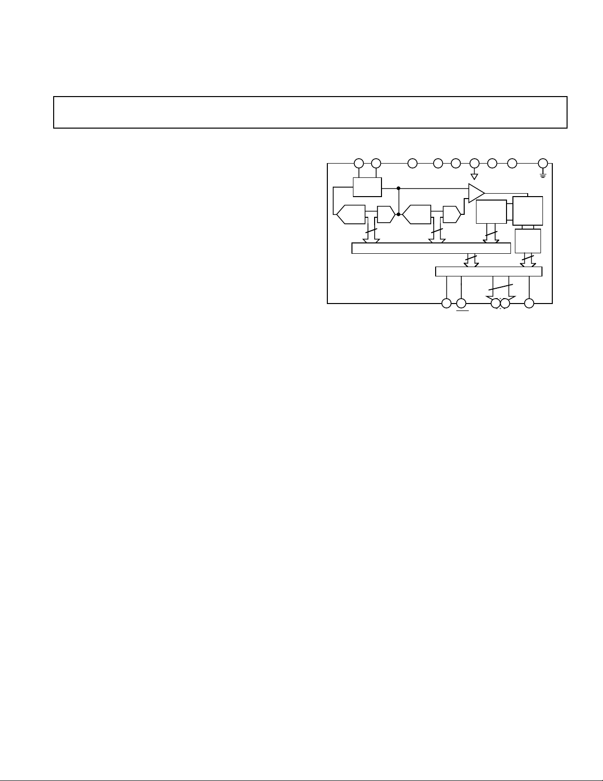
AIN BPO/UPO ENCODE REF IN ACOM DCOM
LATCHES
CORRECTION LOGIC
RANGE
SELECT
X4
COARSE
4-BIT
FLASH
8-BIT
LADDER
MATRIX
FINE
4-BIT
FLASH
AD671
3
4
4
8
12
20
DAC
OTR MSB BIT1-12 DAV
21
16
19
23 22 24
17
18
3-BIT
FLASH
3
DAC
3-BIT
FLASH
14 13 1512 1
V
CC
V
LOGIC
EE
V
Monolithic 12-Bit
a
FEATURES
12-Bit Resolution
24-Pin “Skinny DIP” Package
Conversion Time: 500 ns max—AD671J/K/S-500
Conversion Time: 750 ns max—AD671J/K/S-750
Low Power: 475 mW
Unipolar (0 V to +5 V, 0 V to +10 V) and Bipolar Input
Ranges (65 V)
Twos Complement or Offset Binary Output Data
Out-of-Range Indicator
MIL-STD-883 Compliant Versions Available
PRODUCT DESCRIPTION
The AD671 is a high speed monolithic 12-bit A/D converter
offering conversion rates of up to 2 MHz (500 ns conversion
time). The combination of a merged high speed bipolar/CMOS
process and a novel architecture results in a combination of
speed and power consumption far superior to previously available hybrid implementations. Additionally, the greater reliability
of monolithic construction offers improved system reliability
and lower costs than hybrid designs.
The AD671 uses a subranging flash conversion technique, with
digital error correction for possible errors introduced in the first
part of the conversion cycle. An on-chip timing generator provides strobe pulses for each of the four internal flash cycles and
assures adequate settling time for the interflash residue amplifier. A single ENCODE pulse is used to control the converter.
The performance of the AD671 is made possible by using high
speed, low noise bipolar circuitry in the linear sections and low
power CMOS for the logic sections. Analog Devices’ ABCMOS-1
process provides both high speed bipolar and 2-micron CMOS
devices on a single chip. Laser trimmed thin-film resistors are
used to provide accuracy and temperature stability.
The AD671 is available in two conversion speeds and performance grades. The AD671J and K grades are specified for operation over the 0°C to +70°C temperature range. The AD671S
grades are specified for operation over the –55°C to +125°C
temperature range. All grades are available in a 0.300 inch wide
24-pin ceramic DIP. The J and K grades are also available in a
24-pin plastic DIP.
REV. B
Information furnished by Analog Devices is believed to be accurate and
reliable. However, no responsibility is assumed by Analog Devices for its
use, nor for any infringements of patents or other rights of third parties
which may result from its use. No license is granted by implication or
otherwise under any patent or patent rights of Analog Devices.
2 MHz A/D Converter
AD671
FUNCTIONAL BLOCK DIAGRAM
PRODUCT HIGHLIGHTS
1. The AD671 offers a single chip 2 MHz analog-to-digital
conversion function in a space saving 24-pin DIP.
2. Input signal ranges are 0 V to +5 V and 0 V to +10 V unipolar, and –5 V to +5 V bipolar, selected by pin strapping. Input resistance is 1.5 kΩ. Power supplies are +5 V and –5 V,
and typical power consumption is less than 500 mW.
3. The external +5 V reference can be chosen to suit the dc accuracy and temperature drift requirements of the application.
4. Output data is available in unipolar, bipolar offset or bipolar
twos complement binary format.
5. An OUT OF RANGE output bit indicates when the input
signal is beyond the AD671’s input range.
6. The AD671 is available in versions compliant with the MILSTD-883. Refer to the Analog Devices Military Products
Databook or current AD671/883B data sheet for detailed
specifications.
One Technology Way, P.O. Box 9106, Norwood, MA 02062-9106, U.S.A.
Tel: 617/329-4700 Fax: 617/326-8703

AD671–SPECIFICATIONS
(T
to T
with VCC = +5 V 6 5%, V
MAX
DC SPECIFICATIONS
MIN
unless otherwise noted)
AD671J/S-500 AD671K-500
Parameter Min Typ Max Min Typ Max Units
RESOLUTION 12 12 Bits
ACCURACY (+25°C)
Integral Nonlinearity (INL)
T
to T
MIN
MAX
Differential Nonlinearity (DNL)
T
to T
MIN
No Missing Codes 10 Bits Guaranteed 11 Bits Guaranteed
Unipolar Offset
Bipolar Zero
Gain Error
TEMPERATURE COEFFICIENTS
MAX
l
l
2
3
10 11 Bits
0.1 0.25 0.1 0.25 % FSR
Unipolar Offset 610 610 ppm/°C
Bipolar Zero 615 615 ppm/°C
Gain Error 620 620 ppm/°C
ANALOG INPUT
Input Ranges
Bipolar –5 +5 –5 +5 Volts
Unipolar 0+50+5Volts
0 +10 0 +10 Volts
Input Resistance
10 Volt Range 1.0 1.5 2.0 1.0 1.5 2.0 kΩ
5 Volt Range 0.5 0.75 1.0 0.5 0.75 1.0 kΩ
Input Capacitance 10 10 pF
Reference Input Resistance 2.4 3.5 4.7 2.4 3.5 4.7 kΩ
= +5 V 610%, VEE = –5 V 6 5%, V
LOGIC
= +5.000 V,
REF
64 62 LSB
64 64 LSB
610 610 LSB
POWER SUPPLIES
Power Supply Rejection
V
(+5 V ± 0.25 V) 61 61 LSB
CC
V
(+5 V ± 0.5 V) 61 61 LSB
LOGIC
V
(–5 V ± 0.25 V) 61 61 LSB
EE
4
Operating Voltages
V
V
V
CC
LOGIC
EE
+4.75 +5.25 +4.75 +5.25 Volts
+4.5 +5.5 +4.5 +5.5 Volts
–5.25 –4.75 –5.25 –4.75 Volts
Operating Current
I
CC
I
LOGIC
I
EE
5
46 56 46 56 mA
3 6 3 6 mA
46 56 46 56 mA
POWER CONSUMPTION 475 621 475 621 mW
TEMPERATURE RANGE
Specified (J/K) 0 +70 0 +70 °C
Specified (S) –55 +125 °C
NOTES
1
Adjustable to zero with external potentiometers. See Offset/Gain Calibration section for additional information.
2
Full-scale range (FSR) is 5 V for the 0 V to 5 V range and 10 V for the 0 V to 10 V and –5 V to +5 V ranges.
3
25°C to T
4
Change in gain error as a function of the dc supply voltage.
5
Tested under static conditions. See Figure 12 for typical curves of I
Specifications subject to change without notice.
Specifications shown in boldface are tested on all devices at final electrical test with worst case supply voltages at 0, +25 °C and +70°C. Results from those tests are
used to calculate outgoing quality levels. All min and max specifications are guaranteed, although only those shown in boldface are tested.
and 25°C to T
MIN
MAX
.
vs. Conversion Rate and Output Loading.
LOGIC
–2–
REV. B

AD671
(T
to T
with VCC = +5 V 6 5%, V
MAX
DC SPECIFICATIONS
MIN
unless otherwise noted)
AD671J/S-750 AD671K-750
Parameter Min Typ Max Min Typ Max Units
RESOLUTION 12 12 Bits
ACCURACY (+25°C)
Integral Nonlinearity (INL)
T
T
MIN
MIN
to T
to T
(J) 62 61.5 LSB
MAX
(S) 62.5 LSB
MAX
Differential Nonlinearity (DNL)
T
to T
MIN
No Missing Codes 11 Bits Guaranteed 12 Bits Guaranteed
Unipolar Offset
Bipolar Zero
Gain Error
TEMPERATURE COEFFICIENTS
MAX
l
l
2
3
11 12 Bits
0.1 0.25 0.1 0.25 % FSR
Unipolar Offset 610 610 ppm/°C
Bipolar Zero 615 615 ppm/°C
Gain Error 620 620 ppm/°C
ANALOG INPUT
Input Ranges
Bipolar –5 +5 –5 +5 Volts
Unipolar 0+50+5Volts
0 +10 0 +10 Volts
Input Resistance
10 Volt Range 1.0 1.5 2.0 1.0 1.5 2.0 kΩ
5 Volt Range 0.5 0.75 1.0 0.5 0.75 1.0 kΩ
Input Capacitance 10 10 pF
Reference Input Resistance 2.4 3.5 4.7 2.4 3.5 4.7 kΩ
= +5 V 6 10%, VEE = –5 V 6 5%, V
LOGIC
= +5.000 V,
REF
64 64 LSB
610 610 LSB
POWER SUPPLIES
Power Supply Rejection
V
(+5 V ± 0.25 V) 61 61 LSB
CC
V
(+5 V ± 0.5 V) 61 61 LSB
LOGIC
V
(–5 V ± 0.25 V) 61 61 LSB
EE
4
Operating Voltages
Vcc +4.75 +5.25 +4.75 +5.25 Volts
V
LOGIC
V
EE
+4.5 +5.5 +4.5 +5.5 Volts
–5.25 –4.75 –5.25 –4.75 Volts
Operating Current
I
CC
I
LOGIC
I
EE
5
46 56 46 56 mA
3 6 3 6 mA
46 56 46 56 mA
POWER CONSUMPTION 475 621 475 621 mW
TEMPERATURE RANGE
Specified (J/K) 0 +70 0 +70 °C
Specified (S) –55 +125 °C
NOTES
1
Adjustable to zero with external potentiometers. See Offset/Gain Calibration section for additional information.
2
Full-scale range (FSR) is 5 V for the 0 V to 5 V range and 10 V for the 0 V to 10 V and –5 V to +5 V ranges.
3
25°C to T
4
Change in gain error as a function of the dc supply voltage.
5
Tested under static conditions. See Figure 12 for typical curves of I
Specifications subject to change without notice.
Specifications shown in boldface are tested on all devices at final electrical test with worst case supply voltages at 0, +25 °C and +70°C. Results from those tests are
used to calculate outgoing quality levels. All min and max specifications are guaranteed, although only those shown in boldface are tested.
and 25°C to T
MIN
MAX
.
vs. Conversion Rate and Output Loading.
LOGIC
REV. B
–3–
AD671–SPECIFICATIONS
(For all grades T
DIGITAL SPECIFICATIONS
6
5%, V
REF
Parameter Symbol Min Typ Max Units
LOGIC INPUT
High Level Input Voltage V
Low Level Input Voltage V
High Level Input Current (V
Low Level Input Current (V
= V
IN
= 0 V) I
IN
)I
LOGIC
Input Capacitance C
LOGIC OUTPUTS
High Level Output Voltage (I
Low Level Output Voltage (I
= 0.5 mA) V
OH
= 1.6 mA) V
OL
Output Capacitance C
Specifications shown in boldface are tested on all devices at final electrical test. Results from those tests are used to calculate outgoing quality levels. All min and max
specifications are guaranteed, although only those shown in boldface are tested.
Specifications subject to change without notice.
to T
MIN
, with VCC = +5 V 6 5%, V
MAX
= +5.000 V, unless otherwise noted)
IH
IL
IH
IL
IN
OH
OL
OUT
+2.0 V
–10 +10 µA
–10 +10 µA
+2.4 V
= +5 V 6 10%, VEE = –5 V
LOGIC
+0.8 V
5pF
+0.4 V
5pF
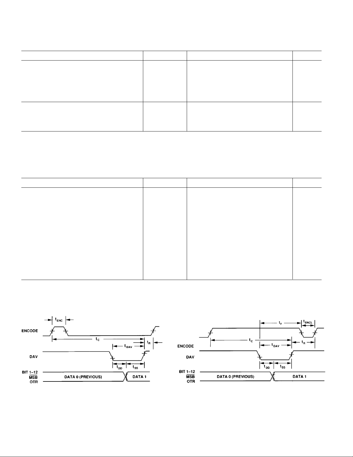
SWITCHING SPECIFICATIONS
(For all grades T
6
5%, VIL = 0.8 V, VIH = 2.0 V, VOL = 0.4 V and VOH = 2.4 V)
MIN
to T
with VCC = +5 V 6 5%, V
MAX
= +5 V 6 10%, VEE = –5 V
LOGIC
Parameter Symbol Min Typ Max Units
Conversion Time
(AD671-500) t
(AD671-750) t
C
C
475 500 ns
725 750 ns
ENCODE Pulse Width High
(AD671-500) t
(AD671-750) t
ENCODE Pulse Width Low t
ENC
ENC
ENCL
20 30 ns
20 50 ns
20 ns
DAV Pulse Width
(AD671-500) t
(AD671-750) t
ENCODE Falling Edge Delay t
Start New Conversion Delay t
Data and OTR Delay from DAV Falling Edge t
Data and OTR Valid before DAV Rising Edge t
NOTES
1
tDD is measured from when the falling edge of DAV crosses 0.8 V to when the output crosses 0.4 V or 2.4 V with a 25 pF load capacitor on each output pin.
2
tSS is measured from when the outputs cross 0.4 V or 2.4 V to when the rising edge of DAV crosses 2.4 V with a 25 pF load capacitor on each output pin.
DAV
DAV
F
R
DD
SS
1
2
75 200 ns
75 300 ns
0ns
0ns
20 75 ns
20 75 ns
a. Encode Pulse HIGH
Figure 1. AD671 Timing Diagrams
–4–
b. Encode Pulse LOW
REV. B
AD671
WARNING!
ESD SENSITIVE DEVICE
ABSOLUTE MAXIMUM RATINGS*
With
Respect
Parameter to Min Max Units
V
CC
V
EE
V
LOGIC
ACOM –0.5 +6.5 Volts
ACOM –6.5 +0.5 Volts
DCOM –0.5 +6.5 Volts
ACOM DCOM –1.0 +1.0 Volts
V
CC
ENCODE DCOM –0.5 V
REF IN ACOM –0.5 V
V
LOGIC
–6.5 +6.5 Volts
+0.5 Volts
LOGIC
+0.5 Volts
CC
AIN, BPO/UPO ACOM –6.5 11.0 Volts
Junction Temperature +175 °C
Storage Temperature –65 +150 °C
l
Model
AD671JD-500 ±4 LSB 0°C to +70°C D-24A
AD671KD-500 ±2 LSB 0°C to +70°C D-24A
AD671JD-750 ±2 LSB 0°C to +70°C D-24A
AD671KD-750 ±1.5 LSB 0°C to +70°C D-24A
AD671SD-500 ±4 LSB –55°C to +125°C D-24A
AD671SD-750 ±2.5 LSB –55°C to +125°C D-24A
NOTES
1
For details on grade and package offerings screened in accordance with
MIL-STD-883, refer to the Analog Devices Military Products Databook or
current AD671/883 data sheet.
2
D = Ceramic DIP.
ORDERING GUIDE
Linearity Range Options
Lead Temperature (10 sec) +300 °C
Power Dissipation 1000 mW
*Stresses above those listed under “Absolute Maximum Ratings” may cause
permanent damage to the device. This is a stress rating only and functional
operation of the device at these or any other conditions above those indicated in the
operational sections of this specification is not implied. Exposure to absolute
maximum ratings for extended periods may effect device reliability.
CAUTION
ESD (electrostatic discharge) sensitive device. Electrostatic charges as high as 4000 V readily
accumulate on the human body and test equipment and can discharge without detection.
Although the AD671 features proprietary ESD protection circuitry, permanent damage may
occur on devices subjected to high energy electrostatic discharges. Therefore, proper ESD
precautions are recommended to avoid performance degradation or loss of functionality.
Temperature Package
2
REV. B
–5–

AD671
AD671 PIN DESCRIPTION
Symbol Pin Type Name and Function
ACOM 22 P Analog Ground.
AIN 20 AI Analog Input Signal.
BIT1 (MSB) 12 DO Most Significant Bit.
BIT2–BIT11 11–2 DO Data Bits 2–11.
BIT12 (LSB) 1 DO Least Significant Bit.
BPO/UPO 21 AI Bipolar or Unipolar
Configuration Pin. Connect to
AIN for 0 V to +5 V Span, to
ACOM for 0 V to +10 V Span
and to REF IN for –5 V to
+5 V Span.
DAV 15 DO Data Available Output. The
Rising Edge of DAV Indicates
an End of Conversion and Can
Be Used to Latch Current
Data into an External
Register. The Falling Edge of
DAV Can Be Used to Latch
Previous Data into an External
Register.
DCOM 18 P Digital Ground.
ENCODE 16 DI The AD671 Starts a
Conversion on the Rising
Edge of the ENCODE Pulse.
MSB 13 DO Inverted Most Significant Bit.
Provides Twos Complement
Output Data Format.
OTR 14 DO Out of Range Is Active HIGH
when the analog input is
beyond the input range of the
converter.
REF IN 19 AI +5 V Reference Input.
V
CC
V
EE
V
LOGIC
TYPE:
AI = Analog Input
DI = Digital Input
DO = Digital Output
P = Power
23 P +5 V Analog Power.
24 P –5 V Analog Power.
17 P +5 V Digital Power.
CONNECTION DIAGRAM
PINOUT
BIT12 (LSB)
BIT1 (MSB)
BIT11
BIT10
BIT9
BIT8
BIT7
BIT6
BIT5
BIT4
BIT3
BIT2
1
2
3
4
5
6
7
(Not to Scale)
8
9
10
11
12
AD671
TOP VIEW
24
23
22
21
20
19
18
17
16
15
14
13
V
EE
V
CC
ACOM
BPO/UPO
AIN
REF IN
DCOM
V
LOGIC
ENCODE
DAV
OTR
MSB
–6–
REV. B

AD671
DEFINITIONS OF SPECIFICATIONS
INTEGRAL NONLINEARITY (INL)
Integral nonlinearity refers to the deviation of each individual
code from a line drawn from “zero” through “full scale.” The
point used as “zero” occurs 1/2 LSB (1.22 mV for a 10 V span)
before the first code transition (all zeros to only the LSB on).
“Full scale” is defined as a level 1 1/2 LSB beyond the last code
transition (to all ones). The deviation is measured from the low
side transition of each particular code to the true straight line.
DIFFERENTIAL NONLINEARITY (DNL, NO MISSING CODES)
An ideal ADC exhibits code transitions that are exactly 1 LSB
apart. DNL is the deviation from this ideal value. Thus every
code must have a finite width. Guaranteed no missing codes to
10-bit resolution indicates that all 1024 codes represented by
Bits 1–10 must be present over all operating ranges. Guaranteed
no missing codes to 11- or 12-bit resolution indicates that all
2048 and 4096 codes, respectively, must be present over all operating ranges.
UNIPOLAR OFFSET
The first transition should occur at a level 1/2 LSB above analog
common. Unipolar offset is defined as the deviation of the actual from that point. This offset can be adjusted as discussed
later. The unipolar offset temperature coefficient specifies the
maximum change of the transition point over temperature, with
or without external adjustments.
GAIN ERROR
The last transition (from 1111 1111 1110 to 1111 1111 1111)
should occur for an analog value 1 1/2 LSB below the nominal
full scale (9.9963 volts for 10.000 volts full scale). The gain error is the deviation of the actual level at the last transition from
the ideal level. The gain error can be adjusted to zero as shown
in Figures 7, 8 and 9.
TEMPERATURE COEFFICIENTS
The temperature coefficients for unipolar offset, bipolar zero
and gain error specify the maximum change from the initial
(+25°C) value to the value at T
MIN
or T
MAX
.
POWER SUPPLY REJECTION
The only effect of power supply error on the performance of the
device will be a small change in gain. The specifications show
the maximum full-scale change from the initial value with the
supplies at the various limits.
SIGNAL-TO-NOISE AND DISTORTION (S/N+D) RATIO
S/N+D is the ratio of the rms value of the measured input signal
to the rms sum of all other spectral components, including harmonics but excluding dc. The value for S/N+D is expressed in
decibels.
EFFECTIVE NUMBER OF BITS (ENOB)
ENOB is calculated from the expression SNR = 6.02N +
1.8 dB, where N is equal to the effective number of bits.
BIPOLAR ZERO
In the bipolar mode the major carry transition (0111 1111 1111
to 1000 0000 0000) should occur for an analog value 1/2 LSB
below analog common. The bipolar offset error and temperature
coefficient specify the initial deviation and maximum change in
the error over temperature.
Theory of Operation
The AD671 uses a successive subranging architecture. The analog to digital conversion takes place in four independent steps or
flashes. The analog input signal is subranged to an intermediate
residue voltage for the final 12-bit result by utilizing multiple
flashes with subtraction DACs (see the AD671 functional block
diagram).
The AD671 can be configured to operate with unipolar (0 V to
+5 V, 0 V to +10 V) or bipolar (±5 V) inputs by connecting
AIN (Pin 20), REFIN (Pin 19) and BPO/UPO (Pin 21) as
shown in Figure 2.
The AD671 conversion cycle begins by simply providing an active HIGH pulse on the ENCODE pin (Pin 16). The rising
edge of the ENCODE pulse starts the conversion. The falling
edge of the ENCODE pulse is specified to operate within a window of time: less than 30 ns after the rising edge of ENCODE
TOTAL HARMONIC DISTORTION (THD)
THD is the ratio of the rms sum of the first six harmonic components to the rms value of the measured input signal and is expressed as a percentage or in decibels.
PEAK SPURIOUS OR PEAK HARMONIC COMPONENT
The peak spurious or peak harmonic component is the largest
spectral component excluding the input signal and dc. This
value is expressed in decibels relative to the rms value of a fullscale input signal.
(AD671-500) and less than 50 ns after the falling edge of
ENCODE (AD671–750) or after the falling edge of DAV. The
time window prevents digitally coupled noise from being introduced during the final stages of conversion. An internal timing
generator circuit accurately controls all internal timing.
ACOM
22
BPO/UPO
AIN
REF IN
0 TO 5V
21
20
19
+
5V REF
+
BPO/UPO
21
AIN
REF IN
0 TO 10V
20
19
+
5V REF
+
AIN AIN
BPO/UPO
AIN
REF IN
–+
5V TO 5V
21
20
AIN
19
+
5V REF
Figure 2. Input Range Connections
REV. B
–7–

AD671
Upon receipt of an ENCODE command, the first 3-bit flash
converts the analog input voltage. The 3-bit result is passed to a
correction logic register and a segmented current output DAC.
The DAC output is connected through a resistor (within the
Range/Span Select Block) to AIN. A residue voltage is created
by subtracting the DAC output from AIN, which is less than
one eighth of the full-scale analog input. The second flash has
an input range that is configured with one bit of overlap with the
previous DAC. The overlap allows for errors during the flash
conversion. The first residue voltage is connected to the second
3-bit flash and to the noninverting input of a high speed, differential, gain-of-four amplifier. The second flash result is passed
to the correction logic register and to the second segmented current output DAC. The output of the second DAC is connected
to the inverting input of the differential amplifier. The differential amplifier output is connected to a two step backend 8-bit
flash. This 8-bit flash consists of coarse and fine flash converters. The result of the coarse 4-bit flash converter, also configured to overlap one bit of DAC 2, is connected to the correction
logic register and selects one of 16 resistors from which the fine
4-bit flash will establish its span voltage. The fine 4-bit flash is
connected directly to the output latches.
The AD671 will flag an out-of-range condition when the input
voltage exceeds the analog input range. OTR (Pin 14) is active
HIGH when an out of range high or low condition exists. Bits
1–12 are HIGH when the analog input voltage is greater than
the selected input range and LOW when the analog input is less
than the selected input range.
APPLYING THE AD671
DRIVING THE AD671 ANALOG INPUT
The AD671 uses a very high speed current output DAC to subtract a known voltage from the analog input. This results in very
fast steps of current at the analog input. It is important to recognize that the signal source driving the analog input of the
AD671 must be capable of maintaining the input voltage under
dynamically-changing load conditions. When the AD671 starts
its conversion cycle, the subtraction DAC will sink up to 5 mA
(see Figure 3) from the source driving the analog input. The
source must respond to this current step by settling the input
voltage back to a fraction of an LSB before the AD671 makes its
final 12-bit decision.
+
–
IIN
IA/D
AD671
R
A/D DAC
IDAC
Figure 3. Driving the Analog Input
Unlike successive approximation A/Ds, where the input voltage
must settle to a fraction of a 12-bit LSB before each successive
bit decision is made, the AD671 requires the analog input voltage settle to within 12 bits before the third flash conversion,
approximately 200 ns. This “free” 200 ns is useful in applications requiring a sample-and-hold amplifier (SHA), overlapping
the SHA’s hold mode settling time within the 200 ns window
will increase total system throughput. See the “Discrete Sampleand-Hold” section for a high speed SHA application.
INPUT BUFFER AMPLIFIER
The closed-loop output impedance of an op amp is equal to the
open loop output impedance (usually a few hundred ohms) divided by the loop gain at the frequency of interest. It is often
assumed that loop gain of a follower-connected op amp is sufficiently high to reduce the closed-loop output impedance to a
negligibly small value, particularly if the input signal is low
frequency. At higher frequencies the open-loop gain is lower,
increasing the output impedance which decreases the instantaneous analog input voltage and produces an error.
The recommended wideband, fast settling input amplifiers for
use with the AD671 are the AD841, AD843, AD845 or the
AD847. The AD841 is unity gain stable and recommended as a
follower connected op amp. The AD843 and AD845 FET inputs make them ideal for high speed sample-and-hold amplifiers
and the AD847 can be used as a low power, high speed buffer.
Figure 4 shows the AD841 driving the AD671. As shown in the
figure the analog input voltage should be produced with respect
to the ACOM pin.
EE
ENCODE
V
17
LOGIC
BIT12
MSB
BIT1
DAV
OTR
1
12
16
15
14
+
±
–
5V
+
5V REF
4
AD841
5
23 24
11
10
6
VCCV
20
AIN
22
ACOM
18
DCOM
19
REF IN
21 13
BPO/UPO
AD671
Figure 4. Input Buffer Amplifier
REFERENCE INPUT
The AD671 uses a standard +5 volt reference. The initial accuracy and temperature stability of the reference can be selected to
meet specific system requirements. Like the analog input, fast
switching input-dependent currents are modulated at the reference input pin (REF IN–Pin 19). However, unlike the analog
input the reference input is held at a constant +5 volts with the
use of capacitor. The recommended reference is the AD586, a
+5 V precision reference with an output buffer amplifier. Figure 5 shows the AD671 configured in the ± 5 V input range.
The 6.8 µF capacitor maintains a constant +5 volts under the
dynamically changing load conditions. An optional 1 µF noise
reduction capacitor can be connected to the AD586, further reducing broadband output noise. To minimize ground voltage
drops the AD586’s ground pin should be tied as close as possible to the AD671’s ACOM pin. See Figures 20, 21 and 22 for
PCB layout recommendations.
–8–
REV. B

AD671
AIN
REF IN
BPO/UPO
ACOM
BIT1
BIT12
DCOM
AD671
ENCODE
DAV
OTR
MSB
20
23 24
17
22
18
19
21
13
14
15
16
VCCV
EE
V
LOGIC
1
12
0.1µF
10µF
10µF10µF
0.1µF 0.1µF
+
5V
+
5V
–
5V
0 TO 10V
+
10µF
0.1µF
10µF
1
14
15
50
1µF
150
13
12 11
8
10
95
7
6
4 3
5k
R2
100k
50
1µF
AD588
0.1µF
150pF
10k
39k
15V
+
2
16
+
15
–
15
R1
100
1µF
C14
AD586
U4
8
NOISE
REDUCTION
GND
23 24
VCCV
20
AIN
±
5V
+
15V
2
+V
IN
V
OUT
6
6.8µF
C15
4
22
ACOM
18
DCOM
19
REF IN
21
BPO/UPO
U3
EE
ENCODE
AD671
V
17
LOGIC
BIT12
DAV
OTR
MSB
BIT1
1
12
16
15
14
13
Figure 5. AD586 as Reference Input for AD671
GROUNDING AND DECOUPLING RULES
Proper grounding and decoupling should be a primary design
objective in any high speed, high resolution system. The AD671
separates analog and digital grounds to optimize the management of analog and digital ground currents in a system. The
AD671 is designed to minimize the current flowing from
ACOM (Pin 22) by directing the majority of the current from
V
(+5 V–Pin 23) to VEE (–5 V–Pin 24). Minimizing analog
CC
ground currents hence reduces the potential for large ground
voltage drops. This can be especially true in systems that do not
utilize ground planes or wide ground runs. ACOM is also configured to be code independent, therefore reducing input dependent analog ground voltage drops and errors. The input current
supplied by the external reference (REFIN–Pin 19) and the majority of the full-scale input signal (AIN–Pin 20) are also directed to V
. Also critical in any high speed digital design are
ÉE
the use of proper digital grounding techniques to avoid potential
CMOS “ground bounce.” Figure 6 is provided to assist in the
proper layout, grounding and decoupling techniques.
Table I is a list of grounding and decoupling guidelines that
should be reviewed before laying out a printed circuit board.
Table I. Grounding and Decoupling Guidelines
Power Supply
Decoupling Comment
Capacitor Values 0.1 µF (Ceramic) and 10 µF (Tantalum).
(Surface Mount Chip Capacitors Recommended to Reduce Lead Inductance).
Capacitor Locations Directly at Positive and Negative
Supply Pins to Respective Ground Plane.
Grounding
Analog Ground Ground Plane or Wide Ground Return
Connected to the Analog Power Supply.
Digital Ground Ground Plane or Wide Ground Return
Connected to the Digital Power Supply.
Analog and Digital
Ground Connected Together Once at the AD671.
UNIPOLAR (0 V TO +10 V) CALIBRATION
The AD671 is factory trimmed to minimize offset, gain and linearity errors. In some applications the offset and gain errors of
the AD671 need to be externally adjusted to zero. This is accomplished by trimming the voltage at BPO/UPO (Pin 21) and
REFIN (Pin 19). In those applications the AD588, a high precision pin programmable voltage reference, is an ideal choice. The
AD588 includes a reference cell and three additional amplifiers
which can be configured to provide offset and gain trims for the
AD671. The circuit in Figure 7 is recommended for calibrating
offset and gain errors of the AD671 when configured in the 0 V
to +10 V input range.
REV. B
0.1µF
10µF
+
5V
–
10µF10µF
0.1µF 0.1µF
5V
+
23 24
EE
ENCODE
BIT12
V
BIT1
DAV
OTR
MSB
LOGIC
VCCV
+
±
V
5V
IN
–
AGP*
+
5V REF
Figure 6. AD671 Grounding and Decoupling
DGP*
*GROUND PLANE RECOMMENDED
20
22
18
19
21
AIN
ACOM
DCOM
REF IN
BPO/UPO
AD671
5V
17
12
1
16
15
14
13
The AD671 is intended to have a nominal 1/2 LSB offset so
that the exact analog input for a given code will be in the middle
Figure 7. Unipolar (0 V to +10 V) Calibration
of that code (halfway between the transitions to the codes above
it and below it). Thus, the first transition ( from 0000 0000 0000
to 0000 0000 0001) will occur for an input level of +1/2 LSB
(1.22 mV for 10 V range). If the offset trim resistor R2 is used,
–9–

AD671
it should be trimmed as above, although a different offset can be
set for a particular system requirement. This circuit will give approximately ±50 mV of offset trim range.
The gain trim is done by applying a signal 1 1/2 LSBs below the
nominal full scale (9.9963 for a 10 V range). Trim R1 to give
the last transition (1111 1111 1110 to 11111111 1111).
UNIPOLAR (0 V TO +5 V) CALIBRATION
The connections for the 0 V to +5 V input range calibration is
shown in Figure 8. The AD586, a +5 V precision voltage reference, is an excellent choice for this mode of operation because
of its performance, stability and optional fine trim. The AD845
(16 MHz, low power, low cost op amp) is used to maintain the
+5 volts under the dynamically changing load conditions of the
reference input.
+15V
1µF
+
15V
2
+V
IN
NOISE
8
REDUCTION
AD586
0 TO +5V
V
OUT
TRIM
GND
4
6
5
–15V
2
3
0.1µF
AD845
4
2
3
10kΩ
7
1
1kΩ
AD845
–15V
7
4
0.1µF
8
+15V
6
390
0.1µF
6
0.1µF
+15V
20
21
22
18
19
23 24
VCCV
AIN
BPO/UPO
ACOM
DCOM
REFIN
AD671
EE
17
V
LOGIC
BIT1
BIT12
ENCODE
DAV
OTR
MSB
12
1
16
15
14
13
Figure 8. Unipolar (0 V to +5 V) Calibration
The AD671 offset error must be trimmed within the analog input path, either directly in front of the AD671 or within the signal conditioning chain, eliminating offset errors induced by the
signal conditioning circuitry. Figure 8 shows an example of how
the offset error can be trimmed in front of the AD671. The
AD586 is configured in the optional fine trim mode to provide
+6%/–2% (+240 LSBs/–80 LSBs) of gain trim. The procedure
for trimming the offset and gain errors is similar to that used for
the unipolar 10 V range with the analog input values set to onehalf the 10 V range values.
BIPOLAR (65 V) CALIBRATION
The connections for the bipolar input range is shown in Figure
9. The AD588 is configured to provide dual +5 V outputs. Providing a +5 V reference voltage for the AD671 gain trim and the
+5 V BPO/UPO input for the bipolar offset trim.
23 24
0.1µF
0.1µF
20
22
18
19
21
VCCV
AIN
ACOM
DCOM
REF IN
BPO/UPO
±
5V
6.2kΩ
+
15V
39k
1µF
6
4 3
7
AD588
12 11810
95
150pF
13
R1
100
50
1
10µF
14
15
2
16
150pF
+
15
–
R2
100
50
10µF
15
EE
AD671
V
BIT1
BIT12
ENCODE
DAV
OTR
MSB
17
LOGIC
12
1
16
15
14
13
Figure 9. Bipolar (±5 V) Calibration
Bipolar calibration is similar to unipolar calibration. First, a signal 1/2 LSB above negative full scale (–4.9988 V) is applied and
R1 is trimmed to give the first transition (0000 0000 0000 to
0000 0000 0001). Then a signal 1 1/2 LSB below positive full
scale (+4.9963) is applied, and R2 is trimmed to give the last
transition (1111 1111 1110 to 1111 1111 1111).
OUTPUT LATCHES
Figure 10 shows the AD671 connected to the 74HC574 Octal
D-type edge triggered latches with 3-state outputs. The latch
can drive highly capacitive loads (i.e., bus lines, I/O ports) while
maintaining the data signal integrity. The maximum set-up and
hold times of the 574 type latch must be less than 20 ns (t
DD
and tSS minimum). To satisfy the requirements of the 574 type
latch the recommended logic families are HC, S, AS, ALS, F or
BCT. New data from the AD671 is latched on the rising edge of
the DAV (Pin 24) output pulse. Previous data can be latched by
inverting the DAV output with a 7404 type inverter. See Figures 20, 21 and 22 for PCB layout recommendations.
BIT10
BIT11
BIT12
AD671
BIT1
BIT2
BIT3
BIT4
BIT5
BIT6
BIT7
BIT8
DAV
BIT9
74HC574
1D
2D
3D
4D
5D
U6
6D
7D
8D
CLK
74HC574
1D
2D
3D
4D
5D
U5
6D
7D
8D
CLK
3Q
OC
5Q
6Q
7Q
8Q
OC
1Q
2Q
4Q
5Q
6Q
7Q
8Q
1Q
2Q
3Q
4Q
DATA BUS
3-STATE
CONTROL
Figure 10. AD671 to Output Latches
OUT OF RANGE
An Out of Range condition exists when the analog input voltage
is beyond the input range (0 V to +5 V, 0 V to +10 V, ±5 V) of
the converter. OTR (Pin 14) is set low when the analog input
voltage is within the analog input range. OTR is set HIGH and
will remain HIGH when the analog input voltage exceeds the
input range by typically 1/2 LSB (OTR transition is tested to
±6 LSBs of accuracy) from the center of the ± full-scale output
codes. OTR will remain HIGH until the analog input is within
the input range and another conversion is completed. By logical
ANDing OTR with the MSB and its complement overrange
high or underrange low conditions can be detected. Table II is a
truth table for the over/under range circuit in Figure 11. Systems requiring programmable gain conditioning prior to the
AD671 can immediately detect an out of range condition, thus
eliminating gain selection iterations.
Table II. Out of Range Truth Table
OTR MSB Analog Input Is
0 0 In Range
0 1 In Range
1 0 Underrange
1 1 Overrange
–10–
REV. B

AD671
MSB
OTR
MSB
OVER = "1"
UNDER = "1"
Figure 11. Overrange or Underrange Logic
OUTPUT DATA FORMAT
The AD671 provides both MSB and MSB outputs, delivering
data in positive true straight binary for unipolar input ranges
and positive true offset binary or twos complement for bipolar
Table III. Output Data Format
Input Analog Digital
Range Coding Input
0 to +5 V Straight Binary ≤ –0.00061 V 0000 0000 0000 1
0 V 0000 0000 0000 0
+5 V 1111 1111 1111 0
>+5.00061 V 1111 1111 1111 1
0 to +10 V Straight Binary ≤ –0.00122 V 0000 0000 0000 1
0 V 0000 0000 0000 0
+10 V 1111 1111 1111 0
≥ +10.00122 V 1111 1111 1111 1
input ranges. Straight binary coding is used for systems that accept positive-only signals. If straight binary coding is used with
bipolar input signals a 0 V input would result in a binary output
of 2048. The application software would have to subtract 2048
to determine the true input voltage. Most processors typically
perform math on signed integers and assume data is in that format. Twos complement format minimizes software overhead
which is especially important in high speed data transfers, such
as a DMA operation. The CPU is not bogged down performing
data conversion steps, hence increasing the total system
throughput.
1
Output OTR
2
–5 V to +5 V Offset Binary ≤ –5.00122 V 0000 0000 0000 1
–5 V 0000 0000 0000 0
0 V 1000 0000 0000 0
+4.99756 V 1111 1111 1111 0
≥ +4.99878 V 1111 1111 1111 1
–5 V to +5 V 2s Complement ≤ –5.00122 V 1000 0000 0000 1
(Using
MSB) –5 V 1000 0000 0000 0
0 V 0000 0000 0000 0
+4.99756 V 0111 1111 1111 0
≥ +4.99878 V 0111 1111 1111 1
NOTES
1
Voltages listed are with offset and gain errors adjusted to zero.
2
Typical performance.
I
vs. CONVERSION RATE
LOGIC
Figure 12 shows the typical logic supply current vs. conversion
rate for various capacitive loads on the digital outputs.
6.5
6.0
5.5
5.0
4.5
4.0
3.5
mA
3.0
2.5
2.0
1.5
1.0
0.5
1k
10k 100k 1M 10M
CONVERSION RATE – Hz
CL = 50pF
CL = 30pF
CL = 0pF
REV. B
Figure 12. I
vs. Conversion Rate for Various
LOGIC
Capacitive Loads on the Digital Outputs
–11–

AD671
AD671
ENCODE
DAV
1/4
7402
1/4
7402
1/4
7402
t
w
HIGH PERFORMANCE SAMPLE-AND-HOLD AMPLIFIER (SHA)
In order to take full advantage of the AD671’s high speed capabilities, a sample-and-hold amplifier (SHA) with fast acquisition
capabilities and rigid accuracy requirements is essential. One
possibility is a hybrid SHA such as the HTC-0300A, but often a
cost effective alternative like the one shown in Figure 13 may be
a better solution. This discrete SHA requires very few components and is able to acquire signals to 0.01% accuracy in less
than 350 nanoseconds. Combined with the AD671, signals with
bandwidths up to 500 kHz can be converted with 12-bit accuracy.
8
9
C29
20pF
VR2 100k
2
3
ADJ
R9
1k
R13
1k
+
U9
AD845
–
15V
15V
C28
20pF
C26
0.1µF
7
4
C27
0.1µF
C34
5pF
R14
226
V
IN
(5Vp–p)
R7
1k
+
15V
C24
R6
2k
S/H
4
5
S/H
U8
AD841
–
15V
0.1µF
11
6
0.1µF
C25
R8
250
10
R11
250
–
15V
R10
10k
2
4
IN1
IN2
5
U10
IN3
13
IN4
12
G1 G2G3G4
3 61411
D1
1N4148
SD5001
OUT1
OUT2
OUT3
OUT4
1
16
PEDESTAL
Figure 13. Discrete High Speed Sample-and-Hold Amplifier
CIRCUIT DESCRIPTION
The discrete SHA shown in Figure 13 is a closed-loop, noninverting architecture which accepts 5 V p-p inputs. The overall
gain of the SHA is +2 in order to accommodate the 10 V input
span of the AD671. The AD841, with a 0.01% settling time of
110 ns, is the suggested input buffer to the SHA. The circuit
also employs a SD5001 which contains four ultrahigh speed
DMOS switches (Q1–Q4). The high CMRR, low input offset
current, and fast settling time of the AD845 op amp are all critical features necessary for optimal performance of the discrete
SHA.
In sample mode, Q1 and Q3 of the SD5001 are closed (Q2 and
Q4 are open). C28 is charged to the input voltage level at a rate
primarily determined by the time constant, R9 • C28. Simultaneously, C29 is connected to ground through a 250 ohm resistor. If C28 is equal to C29, charge injection from Q1 will be
approximately equal to charge injection from Q3 based on the
symmetry of the circuit and the inherent matching of the switch
capacitances. The resultant pedestal errors appear as a commonmode signal to the AD845. VR2, R13, R14, and C34 may be included if further reduction of pedestal error is required.
In hold mode, Q2 and Q4 are closed (Q1 and Q3 are open) to
reduce feedthrough. The input signal is attenuated –78 dB
relative to the input signal at frequencies up to 500 kHz. The
AD845 buffers the voltage on C28 and also provides the wideband, low-impedance output necessary to drive the input of the
AD671.
Droop, which occurs as a result of leakage currents, will appear
on C28 and will similarly appear on C29. Like pedestal errors,
droop appears as a common-mode signal to the AD845 and is
greatly reduced by the differential nature of the circuit. Voltage
droop is typically 5 µV/µs.
CROSS COUPLED LATCH
As noted in the Theory of Operation, the ENCODE pulse is
specified to operate within a window of time. The circuit in Figure 14 can be used to generate a valid ENCODE pulse if a clock
pulse width of greater than 30 ns is available.
Figure 14. Cross Coupled Latch
TIMING DESCRIPTION
6
Figure 15 shows the timing requirements for the discrete SHA.
The complementary S/H inputs are HCMOS-compatible although larger gate voltages will improve performance by lowering the on resistances of the DMOS switches. It should be noted
that a conversion is started before the SHA has settled to 0.01%
accuracy. The discrete SHA takes advantage of the fact that the
AD671 does not require a 12-bit accurate input until it is 150 ns
into its conversion cycle. See Figures 21, 22 and 23 for PCB
layout recommendations.
t
= 1µs
SAMPLE
ENCODE
t
DAV
S/H
CONVERSION
= 500ns
t
ACQUIRE
≈ 350ns
t
SETTLE
350ns
Figure 15. AD671 to Discrete SHA Timing Diagram
DYNAMIC PERFORMANCE
In most sampling applications the dynamic performance of the
system is limited by the performance of the SHA. The SHA’s
dynamic performance can be selected to meet the system sampling requirements. Figures 16 and 17 are typical FFT plots
using the discrete SHA in Figure 13.
Figure 16. Typical FFT Plot of AD671 and Discrete SHA
= 100 kHz
F
IN
–12–
REV. B

Figure 17. Typical FFT Plot of AD671 and Discrete SHA
= 500 kHz
F
IN
MULTICHANNNEL DATA ACQUISITION SYSTEM
The AD684, a quad high speed sample-and-hold amplifier is
ideally suited for multichannel data acquisition applications.
Figure 18 shows a typical data acquisition circuit using the
AD684 (SHA), ADG201HS (Multiplexer), AD588 (Reference)
and the AD671. The AD684 is configured to simultaneously
sample four analog inputs. Each held analog input voltage can
be selected by the multiplexer and buffered by the AD841. The
AD671 is connected in the bipolar input range (± 5 V).
AD671
DYNAMIC CHARACTERISTICS
(@ +25°C, tested using the discrete SHA in Figure 15 with VCC = +5 V,
V
= +5 V, VEE = –5 V, f
LOGIC
SAMPLE
= 1 MSPS)
Model AD671JD-500
Effective Number of Bits (ENOB)
F
= 100 kHz 11.3 Bits
IN
FIN = 490 kHz 11.2 Bits
Signal-to-Noise and Distortion (S/N+D) Ratio
F
= 100 kHz 70 dB
IN
FIN = 490 kHz 68 dB
Total Harmonic Distortion (THD)
F
= 100 kHz –80 dB
IN
FIN = 490 kHz –75 dB
Peak Spurious (dc to 490 kHz) –79 dB
Peak Harmonic Component (dc to 490 kHz) –76 dB
NOTE
1
fIN amplitude = –0.2 dB @ 100 kHz and –0.9 dB @ 490 kHz, bipolar mode
unless otherwise indicated. See Definition of Specifications for additional
information.
1
Typ Units
REV. B
Figure 18. Data Acquisition System Using the AD684 and the AD671
–13–

AD671
ADSP-2101
A0:13
D0:15
ADDRESS BUS
DECODE
Q0:7
D0:7
574
OE
Q0:7
D0:7
574
OE
DATA BUS
D0:3
DAV
BIT1:12
SAMPLING
CLOCK
ENCODE
16
8
4
8
8
4
RD
IRQ2
AD671
AD671 TO ADSP-2100A INTERFACE
Figure 19 demonstrates the AD671 to ADSP-2100A interface.
The 2100A with a clock frequency of 12.5 MHz can execute an
instruction in one 80 ns cycle. The AD671 is configured to perform continuous time sampling. The DAV output of the AD671
is asserted at the end of each conversion. DAV can be used to
latch the conversion result into the two 574 octal D-latches. The
falling edge of the sampling clock is used to generate an interrupt (IRQ3) for the processor. Upon interrupt, the ADSP2100A starts a data memory read by providing an address on
the DMA bus. The decoded address generates OE for the
latches and the processor reads their output over the DMA bus.
The conversion result is read within a single processor cycle.
AD671 TO ADSP-2101/ADSP-2102 INTERFACE
Figure 20 is identical to the 2100A interface except the sampling clock is used to generate an interrupt (IRQ2) for the processor. Upon interrupt the ADSP-2101A starts a data memory
read by providing an address on the Address (A) bus. The decode address generates
OE for the D-latches and the processor
reads their output over the Data (D) bus. Reading the conversion result is thus completed within a single processor cycle.
DMRD
DMA0:13
ADSP-2100A
DMA0:15
DMACK
IRQ3
ADDRESS BUS
DECODE
16
DATA BUS
+
5V
SAMPLING
CLOCK
OE
574
8
Q0:7
OE
574
8
Q0:7
Figure 19. AD671 to ADSP-2100A Interface
D0:7
D0:3
D0:7
DAV
AD671
8
BIT1:12
4
4
ENCODE
Figure 20. AD671 to ADSP-2101/ADSP-2102 Interface
Figure 21. PCB Silkscreen and Component Placement
Diagram for Figures 5, 10 and 13
–14–
REV. B

Figure 22. PCB Solder Side Layout for Figures 5, 10 and 13
AD671
REV. B
Figure 23. PCB Component Side Layout for Figures 5, 10 and 13
–15–

AD671
OUTLINE DIMENSIONS
Dimensions shown in inches and (mm).
24-Pin Plastic DIP (Suffix N)
C1426a–10–9/91
SEATING
PLANE
PIN 1
0.175
(4.45)
24-Pin Ceramic DIP (Suffix D)
0.295 6 0.01
1
1.200 6 0.012
(30.48 6 0.31)
0.018 6 0.002
(0.46 6 0.05)
TYP
NOTES
1. LEAD NO. 1 IDENTIFIED BY DOT OR NOTCH.
2. CERAMIC DIP LEADS WILL BE EITHER GOLD OR TIN PLATED
IN ACCORDANCE WITH MIL-M-385 TO REQUIREMENTS.
0.100 6 0.005
(2.54 6 0.13)
1.100 6 0.005
(27.94 6 0.13)
TOLL NON ACCUM
0.05 (1.27)
TYP
(7.49 6 0.26)
0.085 6 0.009
(2.16 6 0.23)
0.300 6 0.010
(7.49 6 0.25)
+ 0.002
0.010
–0.001
0.025
–0.03
(
+ 0.05
)
PRINTED IN U.S.A.
–16–
REV. B
 Loading...