Analog Devices AD668SQ, AD668KQ, AD668JQ, AD668AQ Datasheet

12-Bit Ultrahigh Speed
a
FEATURES
Ultrahigh Speed: Current Settling to 1 LSB in 90 ns for
a Full-Scale Change in Digital Input. Voltage Settling
to 1 LSB in 120 ns for a Full-Scale Change in Analog
Input
15 MHz Reference Bandwidth
Monotonicity Guaranteed over Temperature
10.24 mA Current Output or 1.024 V Voltage Output
Integral and Differential Linearity Guaranteed over
Temperature
0.3" “Skinny DIP” Packaging
MIL-STD-883 Compliant Versions Available
PRODUCT DESCRIPTION
The AD668 is an ultrahigh speed, 12-bit, multiplying digital-toanalog converter, providing outstanding accuracy and speed performance in responding to both analog and digital inputs. The
AD668 provides a level of performance and functionality in a
monolithic device that exceeds that of many contemporary hybrid devices. The part is fabricated using Analog Devices’
Complementary Bipolar (CB) Process, which features vertical
NPN and PNP devices on the same chip without the use of
dielectric isolation. The AD668’s design capitalizes on this proprietary process in combination with standard low impedance
circuit techniques to provide its unique combination of speed
and accuracy in a monolithic part.
The wideband reference input is buffered by a high gain, closed
loop reference amplifier. The reference input is essentially a 1 V,
high impedance input, but trimmed resistive dividers are provided to readily accommodate 5 V and 1.25 V references. The
reference amplifier features an effective small signal bandwidth
of 15 MHz and an effective slew rate of 3% of full scale/ns.
Multiple matched current sources and thin film ladder techniques are combined to produce bit weighting. The output range
can nominally be taken as a 10.24 mA current output or a 1.024 V
voltage output. Varying the analog input can provide modulation
of the DAC full scale from 10% to 120% of its nominal value.
Bipolar outputs can be realized through pin-strapping to provide
two-quadrant operation without additional external circuitry.
Laser wafer trimming insures full 12-bit linearity and excellent
gain accuracy. All grades of the AD668 are guaranteed monotonic over their full operating temperature range. Furthermore,
the output resistance of the DAC is trimmed to 100 Ω ± 1.0%.
Multiplying D/A Converter
AD668
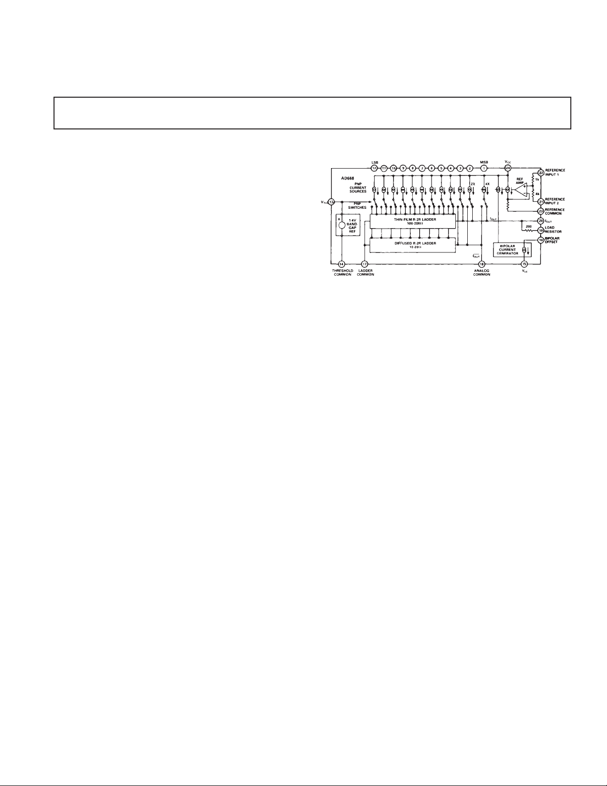
FUNCTIONAL BLOCK DIAGRAM
The AD668 is available in four performance grades. The
AD668JQ and KQ are specified for operation from 0°C to
+70°C, the AD668AQ is specified for operation from –40°C to
+85°C, and the AD668SQ specified for operation from –55°C
to +125°C. All grades are available in a 24-pin cerdip (0.3"
package.
PRODUCT HIGHLIGHTS
1. The fast settling time of the AD668 provides suitable performance for waveform generation, graphics display, and high
speed A/D conversion applications.
2. The high bandwidth reference channel allows high frequency
modulation between analog and digital inputs.
3. The AD668’s design is configured to allow wide variation of
the analog input, from 10% to 120% of its nominal value.
4. The AD668’s combination of high performance and tremendous flexibility makes it an ideal building block for a variety
of high speed, high accuracy instrumentation applications.
5. The digital inputs are readily compatible with both TTL and
5 V CMOS logic families.
6. Skinny DIP (0.3") packaging minimizes board space requirements and eases layout considerations.
7. The AD668 is available in versions compliant with MILSTD-883. Refer to the Analog Devices Military Products
Databook or current AD668/883B data sheet for detailed
specifications.
REV. A
Information furnished by Analog Devices is believed to be accurate and
reliable. However, no responsibility is assumed by Analog Devices for its
use, nor for any infringements of patents or other rights of third parties
which may result from its use. No license is granted by implication or
otherwise under any patent or patent rights of Analog Devices.
One Technology Way, P.O. Box 9106, Norwood, MA 02062-9106, U.S.A.
Tel: 617/329-4700 Fax: 617/326-8703

AD668–SPECIFICA TIONS
(@ TA = +258C, VCC = +15 V, VEE = –15 V, unless otherwise noted)
AD668J/A AD668K AD668S
Parameter Min Typ Max Min Typ Max Min Typ Max Units
RESOLUTION 12 12 12 Bits
LSB WEIGHT (At Nominal FSR)
Current 2.5 * * µA
Voltage (Current into RL) 250 * * µV
ACCURACY
1
Linearity –1/2 +1/2 –1/4 +1/4 * * LSB
T
MIN
to T
MAX
–3/4 +3/4 –1/2 +1/2 * * LSB
Differential Nonlinearity –1 +1 –1/2 +1/2 * * LSB
T
MIN
to T
MAX
–1 +1 –1/2 +1/2 * * LSB
Monotonicity GUARANTEED OVER RATED SPECIFICATION TEMPERATURE RANGE
Unipolar Offset (Digital) –0.2 +0.2 * * * * % of FSR
Bipolar Offset –1.0 +1.0 –0.6 +0.6 * * % of FSR
Bipolar Zero –0.5 +0.5 –0.2 +0.2 * * % of FSR
Analog Offset –1.0 +1.0 –0.7 +0.7 * * % of V
NOM
Gain Error –1.0 +1.0 * * * * % of FSR
TEMPERATURE COEFFICIENTS
2
Unipolar Offset –8 +8 –5 +5 * * ppm of FSR/°C
Bipolar Offset –25 +25 –15 +15 * * ppm of FSR/°C
Bipolar Zero –20 +20 –15 +15 * * ppm of FSR/°C
Analog Offset –20 +20 –10 +10 –20 +20 ppm of V
NOM
Gain Drift –30 +30 –15 +15 –40 +40 ppm of FSR/°C
Gain Drift (I
) ±150 ±150 ±150 ppm of FSR/°C
OUT
REFERENCE INPUT
Input Resistance
5.0 V Range 5 * * kΩ
1.25 V Range 5 * * kΩ
1.0 V Range 1 * * MΩ
Reference Range (T
MIN
to T
) 10 100 120 * * * * * * % of V
MAX
NOM
DATA INPUTS
Logic Levels (T
V
IH
V
LL
Logic Currents (T
I
IH
I
IL
MIN
to T
MIN
MAX
to T
)
MAX
2.0 7.0 * * * * V
0.0 0.8 ****V
)
–10 +10 ****µA
0 60 100 *** 0 100 200 –µA
VTH Pin Voltage 1.4 V
/°C
/°C
CODING BINARY, OFFSET BINARY
CURRENT OUTPUT RANGES 0 to 10.24, ± 5.12 mA
VOLTAGE OUTPUT RANGES 0 to 1.024, ± 0.512 V
OUTPUT COMPLIANCE –2 +1.2 * * * * V
OUTPUT RESISTANCE
Exclusive of R
Inclusive of R
L
L
160 200 240 * * * * * * Ω
99 100 101 * * * * * * Ω
REFERENCE AMPLIFIER
Input Bias Current 1.5 * * µA
Slew Rate 3 * * % of FS/ns
Large Signal Bandwidth 10 * * MHz
Small Signal Bandwidth 15 * * MHz
Undervoltage Recovery Time
V
REF/VNOM
to 0% 35 * * ns
–2–
REV. A

AD668J/A AD668K AD668S
Parameter Min Typ Max Min Typ Max Min Typ Max Units
AC CHARACTERISTICS
Analog Settling Time
(10% to 120% Step)
to ±1% 60 * * ns to 1% of FSR
to ±0.1% 90 * * ns to 0.1% of FSR
to ±0.025% 120 * * ns to 0.025% of FSR
Digital Settling Time
Current
to ± 1% 30 * * ns to 1% of FSR
to ±0.025% 90 * * ns to 0.025% of FSR
Voltage (100 Ω Internal R
3
)
L
to 1% 50 * * ns to 1% of FSR
to 0.1% 75 * * ns to 0.1% of FSR
to 0.025% 110 * * ns to 0.025% of FSR
Glitch Impulse
Peak Amplitude 20 * * % of FSR
Total Harmonic Distortion
Multiplying Feedthrough Error
FULL-SCALE TRANSITION
4
5
6
2
350 * * pV-sec
–75 * * dB
–62 * * dB
10% to 90% Rise Time 11 * * ns
90% to 10% Fall Time 11 * * ns
AD668
POWER REQUIREMENTS
+10.8 V to +16.5 V 27 32 **mA
–10.8 V to –16.5 V 7 9 * * –mA
Power Dissipation 510 615 * * mW
7
PSRR
TEMPERATURE RANGE
Rated Specification
2
(J, K, S) 0 +70 * * –55 +125 °C
0.05 * * % of FSR/V
Rated Specification (A) –40 +85 °C
Storage –65 +150 * * * * °C
NOTES
*Same as AD668J/A.
1
Measured in I
2
Measured in V
full-scale reference.
3
Total resistance. Refer to Figure 4.
4
At the major carry, driven by HCMOS logic.
mode. Specified at nominal 5 V full-scale reference.
OUT
mode, unless otherwise specified. Specified at nominal 5 V
OUT
ABSOLUTE MAXIMUM RATINGS*
VCC to REFCOM . . . . . . . . . . . . . . . . . . . . . . . . 0 V to +18 V
V
to REFCOM . . . . . . . . . . . . . . . . . . . . . . . . . .0 V to –18 V
EE
REFCOM to LCOM . . . . . . . . . . . . . . . . . . +100 mV to –10 V
ACOM to LCOM . . . . . . . . . . . . . . . . . . . . . . . . . . . ±100 mV
THCOM to LCOM . . . . . . . . . . . . . . . . . . . . . . . . . . ±500 mV
REFCOM to REFIN (1, 2) . . . . . . . . . . . . . . . . . . . . . . . .18 V
I
to LCOM . . . . . . . . . . . . . . . . . . . . . . . . . . . . . . . . . .±5 V
BPO
I
to LCOM . . . . . . . . . . . . . . . . . . . . . . . . . . . . –5 V to V
OUT
Digital Inputs to THCOM . . . . . . . . . . . . . –500 mV to +7.0 V
REFIN1 to REFIN2 . . . . . . . . . . . . . . . . . . . . . . . . . . . . .36 V
V
to THCOM . . . . . . . . . . . . . . . . . . . . . . –0.7 V to +1.4 V
TH
5
V
= 1 V p-p, VIN = 10% to 110%, 100 kHz. Digital Input All 1s.
OUT
6
VIN = 200 mV p-p, 1 MHz Sine Wave. Digital Input all 0s. See Figure 20.
7
Measured at 15 V ± 10% and 12 V ±10%.
Specifications shown in boldface are tested on all producfion units at final electrical test.
Specifications subject to change without notice.
Power Dissipation . . . . . . . . . . . . . . . . . . . . . . . . . . . .670 mW
Storage Temperature Range
Q (Cerdip) Package . . . . . . . . . . . . . . . . . .–65°C to +150°C
Junction Temperature . . . . . . . . . . . . . . . . . . . . . . . . . +175°C
Thermal Resistance
θ
. . . . . . . . . . . . . . . . . . . . . . . . . . . . . . . . . . . . . +75°C/W
JA
θ
. . . . . . . . . . . . . . . . . . . . . . . . . . . . . . . . . . . . . +25°C/W
JC
*Stresses above those listed under “Absolute Maximum Ratings” may cause
permanent damage to the device. This is a stress rating only and functional
TH
operation of the device at these or any other conditions above those indicated in the
operational sections of this specification is not implied. Exposure to absolute
maximum rating conditions for extended periods may affect device reliability.
Logic Threshold Control Input Current . . . . . . . . . . . . . 5 mA
REV. A
–3–

AD668
ORDERING GUIDE
Linearity Voltage
Temperature Error Max Gain T.C. Package
Range @ 25°C Max ppm/°C Option
2
Model
1
AD668JQ 0°C to +70°C ±1/2 ±30 Q-24
AD668KQ 0°C to +70°C ± 1/4 ±15 Q-24
AD668AQ –40°C to +85°C ± 1/2 ±30 Q-24
AD668SQ –55°C to +125°C ±1/2 ±40 Q-24
NOTES
1
For details on grade and package offerings screened in accordance with MIL-STD-883, refer to the
Analog Devices Military Products Databook or current AD668/883B data sheet.
2
Q = Cerdip.
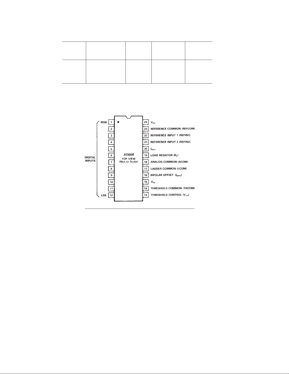
PIN CONFIGURATION
DEFINITIONS
LINEARITY ERROR (also called INTEGRAL NONLINEARITY OR INL): Analog Devices defines linearity error as the
maximum deviation of the actual analog output from the ideal
output (a straight line drawn from 0 to FS) for any bit combination expressed in multiples of 1 LSB. The AD668 is laser
trimmed to 1/4 LSB (0.006% of FS) maximum linearity error at
+25°C for the K version and 1/2 LSB for the J and S versions.
DIFFERENTIAL LINEARITY ERROR (also called DIFFERENTIAL NONLINEARITY or DNL): DNL is the measure of
the variation in the analog output, normalized to fun scale, associated with a 1 LSB change in digital input code.
MONOTONICITY: A DAC is said to be monotonic if the output either increases or remains constant as the digital input increases. Monotonic behavior requires that the differential
linearity error not exceed 1 LSB in the negative direction.
UNIPOLAR OFFSET ERROR (DAC OFFSET): The DAC
offset is the portion of the DAC output that is independent of
the digital input. The unipolar DAC offset error is measured as
the deviation of the analog output from the ideal (0 V or 0 mA)
when the analog input is set to 100% and the digital inputs are
set to all 0s.
BIPOLAR OFFSET ERROR: The deviation of the analog output from the ideal (negative half-scale) when the DAC is connected in the bipolar mode (Pin 16 connected to Pin 20), the
analog input is set to 100%, and the digital inputs are set to all
0s is called the bipolar offset error.
BIPOLAR ZERO ERROR: The deviation of the analog output
from the ideal (0 V or 0 mA) for bipolar mode when only the
MSB is on (100 . . . 00) is called bipolar zero error.
COMPLIANCE VOLTAGE: The allowable voltage excursion
at the output node of a DAC which will not degrade the accuracy of the DAC output.
SETTLING TIME (DIGITAL CHANNEL): The time required for the output to reach and remain within a specified
error band about its final value, measured from the digital input
transition.
SETTLING TIME (ANALOG CHANNEL): The time required for the output to reach and remain within a specified error band about its final value, measured from the analog input’s
crossing of it’s 50% value.
GAIN ERROR: The difference between the ideal and actual
output span of FS – 1 LSB, expressed either in % of FS or LSB,
when all bits are on is called the gain error.
–4–
REV. A

AD668
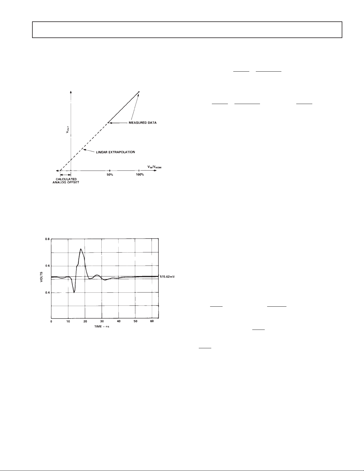
ANALOG OFFSET ERROR: The analog offset is defined as
the offset of the analog amplifier channel, referred to the analog
input. Ideally, this would be measured with the analog input at
0 V and the digital input at full scale. Since a 0 V analog input
voltage constitutes an undervoltage condition, this specification
is determined through linear extrapolation, as indicated in
Figure 1.
Figure 1. Derivation of Analog Offset Voltage
GLITCH IMPULSE: Asymmetrical switching times in a DAC
may give rise to undesired output transients which are quantified by their glitch impulse. It is specified as the net area of the
glitch in pV-sec.
In current output mode:
Unipolar Mode
I
OUT
V
=
V
NOM
IN
DAC code
×
4096
×10.24 mA
Bipolar Mode
I
OUT
V
=
V
NOM
IN
DAC code
×
4096
×10.24 mA –
V
V
NOM
IN
× 5.12 mA
In voltage output mode:
V
= I
OUT
OUT
× R
LOAD
(for both unipolar and bipolar modes)
where:
– the analog input voltage.
V
IN
– the nominal full scale of the reference voltage: 1 V,
V
NOM
1.25 V, or 5 V, determined by the wiring configuration of Pins
21 and 22. (See APPLYING THE AD668.)
DAC code – the numerical representation of the DAC’s digital
inputs; a number between 0 and 4095.
R
– the resistance of the DAC output node; the maximum
LOAD
this can be is 200 Ω (the internal DAC ladder resistance). The
on-board load resistor (Pin 19) has been trimmed so that its
parallel combination with the DAC ladder resistance is 100 Ω
(±1%)
Bipolar mode – produces a bipolar analog output from the digital
input by offsetting the normal output current with a precision
current source. This offset is achieved by connecting Pin 16 to
the DAC output. In the unipolar mode, Pin 16 should be
grounded.
If the dc errors are included, the transfer function becomes
somewhat more complex:
Figure 2. AD668 Major Carry Glitch
FUNCTIONAL DESCRIPTION
The AD668 is designed to combine excellent performance with
maximum flexibility. The functional block diagram and the
simple transfer functions provided below will provide the user
with a basic grasp of the AD668’s operation. Examples of typical circuit configurations are provided in the section APPLYING THE AD668. Subsequent sections contain more detailed
information useful in optimizing DAC performance in high
speed, high resolution applications.
DAC Transfer Function
The AD668 may be used either in a current output mode (DAC
output connected to a virtual ground) or a voltage output mode
(DAC output connected to a resistive load).
REV. A
–5–
V
V
V
NOM
=
V
IN
IN
+OFFSET
NOM
+OFFSET
+OFFSET
DIGITAL
ANALOG
ANALOG
×
I
OUT
–
(Last term is for use in bipolar mode; V
)
R
LOAD
DAC code
×
V
IN
×10.24 mA
V
NOM
×(5.12 mA +[OFFSET
×(1+ E ) ×10.24 mA
4096
OUT
where:
OFFSET
OFFSET
OFFSET
= the analog offset error.
ANALOG
= is the unipolar digital offset error.
DIGITAL
= is the bipolar offset error.
BIPOLAR
E = the gain error, expressed fractionally.
Operating Limits:
×10.24 mA])
BIPOLAR
is still just I
OUT
×
 Loading...