

Microprocessor-Compatible
a
FEATURES
Complete 12-Bit D/A Function
Double-Buffered Latch
On Chip Output Amplifier
High Stability Buried Zener Reference
Single Chip Construction
Monotonicity Guaranteed Over Temperature
Linearity Guaranteed Over Temperature: 1/2 LSB max
Settling Time: 3 ms max to 0.01%
Guaranteed for Operation with 612 V or 615 V
Supplies
Low Power: 300 mW Including Reference
TTL/5 V CMOS Compatible Logic Inputs
Low Logic Input Currents
MIL-STD-883 Compliant Versions Available
PRODUCT DESCRIPTION
The AD667 is a complete voltage output 12-bit digital-to-analog
converter including a high stability buried Zener voltage reference and double-buffered input latch on a single chip. The
converter uses 12 precision high speed bipolar current steering
switches and a laser trimmed thin-film resistor network to provide fast settling time and high accuracy.
Microprocessor compatibility is achieved by the on-chip doublebuffered latch. The design of the input latch allows direct interface to 4-, 8-, 12-, or 16-bit buses. The 12 bits of data from the
first rank of latches can then be transferred to the second rank,
avoiding generation of spurious analog output values. The latch
responds to strobe pulses as short as 100 ns, allowing use with
the fastest available microprocessors.
The functional completeness and high performance in the
AD667 results from a combination of advanced switch design,
high speed bipolar manufacturing process, and the proven laser
wafer-trimming (LWT) technology. The AD667 is trimmed at
the wafer level and is specified to ± 1/4 LSB maximum linearity
error (K, B grades) at +25°C and ±1/2 LSB over the full operating temperature range.
The subsurface (buried) Zener diode on the chip provides a low
noise voltage reference which has long-term stability and temperature drift characteristics comparable to the best discrete reference diodes. The laser trimming process which provides the
excellent linearity, is also used to trim the absolute value of the
reference as well as its temperature coefficient. The AD667 is
thus well suited for wide temperature range performance with
±1/2 LSB maximum linearity error and guaranteed monotonicity over the full temperature range. Typical full-scale gain TC is
5 ppm/°C.
12-Bit D/A Converter
AD667*
FUNCTIONAL BLOCK DIAGRAM
The AD667 is available in five performance grades. The
AD667J and K are specified for use over the 0°C to +70°C temperature range and are available in a 28-pin molded plastic DIP
(N) or PLCC (P) package. The AD667S grade is specified for
the –55°C to +125°C range and is available in the ceramic DIP
(D) or LCC (E) package. The AD667A and B are specified for
use over the –25°C to +85°C temperature range and are available in a 28-pin hermetically sealed ceramic DIP (D) package.
PRODUCT HIGHLIGHTS
1. The AD667 is a complete voltage output DAC with voltage
reference and digital latches on a single IC chip.
2. The double-buffered latch structure permits direct interface
to 4-, 8-, 12-, or 16-bit data buses. All logic inputs are TTL
or 5 volt CMOS compatible.
3. The internal buried Zener reference is laser-trimmed to 10.00
volts with a ±1% maximum error. The reference voltage is
also available for external application.
4. The gain setting and bipolar offset resistors are matched to
the internal ladder network to guarantee a low gain temperature coefficient and are laser-trimmed for minimum full-scale
and bipolar offset errors.
5. The precision high speed current steering switch and on-board
high speed output amplifier settle within 1/2 LSB for a 10 V
full-scale transition in 2.0 µs as when properly compensated.
6. The AD667 is available in versions compliant with MILSTD-883. Refer to the Analog Devices Military Products
Databook or current AD667/883B data sheet for detailed
specifications.
*Protected by Patent Numbers 3,803,590; 3,890,611; 3,932,863; 3,978,473;
4,020,486; and others pending.
REV. A
Information furnished by Analog Devices is believed to be accurate and
reliable. However, no responsibility is assumed by Analog Devices for its
use, nor for any infringements of patents or other rights of third parties
which may result from its use. No license is granted by implication or
otherwise under any patent or patent rights of Analog Devices.
One Technology Way, P.O. Box 9106, Norwood, MA 02062-9106, U.S.A.
Tel: 617/329-4700 Fax: 617/326-8703
AD667–SPECIFICATIONS
(@ TA = +258C, 612 V, 615 V power supplies unless otherwise noted)
Model AD667J AD667K
Min Typ Max Min Typ Max Units
DIGITAL INPUTS
Resolution 12 12 Bits
Logic Levels (TTL, Compatible, T
VIH (Logic “l’’) +2.0 +5.5 +2.0 +5.5 V
MIN–TMAX
1
)
VIL (Logic “0”) 0 +0.8 0 +0.8 V
IIH (VIH = 5.5 V) 3 10 3 10 µA
IIL (VIL = 0.8 V) 1 5 1 5 µA
TRANSFER CHARACTERISTICS
ACCURACY
Linearity Error @ +25°C +1/4 61/2 ±1/8 61/4 LSB
TA = T
Differential Linearity Error @ +25°C ± 1/2 63/4 ±1/4 61/2 LSB
TA = T
Gain Error
Unipolar Offset Error
Bipolar Zero
MIN
2
MIN
to T
2
to T
MAX
MAX
2
±1/2 63/4 ±1/4 61/2 LSB
Monotonicity Guaranteed Monotonicity Guaranteed LSB
±0.1 60.2 ±0.1 60.2 % FSR
±1 62 ±1 62 LSB
±0.05 60.1 ±0.05 60.1 % of FSR
3
DRIFT
Differential Linearity ± 2 ± 2 ppm of FSR/°C
Gain (Full Scale) TA = 25°C to T
Unipolar Offset TA = –25°C to T
Bipolar Zero TA = 25°C to T
MIN
MIN
MIN
or T
or T
or T
MAX
MAX
MAX
±5 ±30 ±5 ±15 ppm of FSR/°C
±1 ±3 ±3 ppm of FSR/°C
±5 ±10 ±10 ppm of FSR/°C
CONVERSION SPEED
Settling Time to ±0.01% of FSR for
FSR Change (2 kΩi500 pF Load)
with 10 kΩ Feedback 3 4 3 4 µs
with 5 kΩ Feedback 2 3 2 3 µs
For LSB Change 1 1 µs
Slew Rate 10 10 V/µs
ANALOG OUTPUT
Ranges
4
±2.5, ± 5, ± 10, ±2.5, ± 5, ±10, V
+5, +10 +5, +10
Output Current ±5 ±5mA
Output Impedance (DC) 0.05 0.05 Ω
Short Circuit Current 40 40 mA
REFERENCE OUTPUT 9.90 10.00 10.10 9.90 10.00 10.10 V
External Current 0.1 1.0 0.1 1.0 mA
POWER SUPPLY SENSITIVITY
VCC = +11.4 V to +16.5 V dc 5 10 5 10 ppm of FS/%
VEE = –11.4 V to –16.5 V dc 5 10 5 10 ppm of FS/%
POWER SUPPLY REQUIREMENTS
Rated Voltages ±12, ±15 ± 12, ±15 V
4
Range
611.4 616.5 611.4 616.5 V
Supply Current
+11.4 V to +16.5 V dc 8 12 8 12 mA
–11.4 V to –16.5 V dc 20 25 20 25 mA
TEMPERATURE RANGE
Specification 0 +70 0 +70 °C
Storage –65 +125 –65 +125 °C
NOTES
1
The digital input specifications are 100% tested at +25°C, and guaranteed but not tested over the full temperature range.
2
Adjustable to zero.
3
FSR means “Full-Scale Range” and is 20 V for ±10 V range and 10 V for the ±5 V range.
4
A minimum power supply of ±12.5 V is required for a ±10 V full-scale output and ±11.4 V is required for all other voltage ranges.
Specifications subject to change without notice.
Specifications shown in boldface are tested on all production units at final electrical
test. Results from those tests are used to calculate outgoing quality levels. All min and
max specifications are guaranteed, although only those shown in boldface are tested
on all production units.
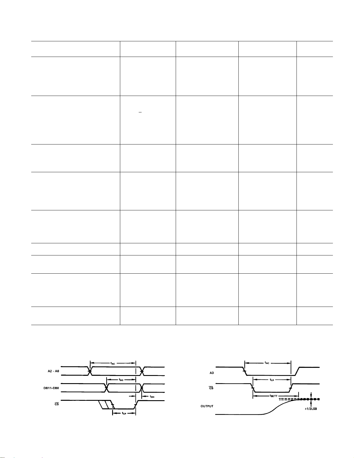
TIMING SPECIFICATIONS
(All Models, TA = +25°C, VCC = +12 V or +15 V, VEE = –12 V or –15 V)
Symbol Parameter Min Typ Max
t
DC
t
AC
t
CP
t
DH
t
SETT
Data Valid to End of CS 50 – – ns
Address Valid to End of CS 100 _ _ ns
CS Pulse Width 100 – – ns
Data Hold Time 0 – – ns
Output Voltage Settling Time – 2 4 µs
ABSOLUTE MAXIMUM RATINGS
VCC to Power Ground . . . . . . . . . . . . . . . . . . . . . 0 V to +18 V
V
to Power Ground . . . . . . . . . . . . . . . . . . . . . 0 V to –18 V
EE
Digital Inputs (Pins 11–15, 17–28)
to Power Ground . . . . . . . . . . . . . . . . . . . . –1.0 V to +7.0 V
Ref In to Reference Ground . . . . . . . . . . . . . . . . . . . . . . ±12 V
Bipolar Offset to Reference Ground . . . . . . . . . . . . . . . . ±12 V
10 V Span R to Reference Ground . . . . . . . . . . . . . . . . . ±12 V
20 V Span R to Reference Ground . . . . . . . . . . . . . . . . . ±24 V
Ref Out, V
. . . . . . . . . . . . . . . . . . . . . . . . . . . Momentary Short to V
(Pins 6, 9) . . Indefinite Short to Power Ground
OUT
CC
Power Dissipation . . . . . . . . . . . . . . . . . . . . . . . . . . 1000 mW
–2–
REV. A
AD667
Model AD667A AD667B AD667S
Min Typ Max Min Typ Max Min Typ Max Units
DIGITAL INPUTS
Resolution 12 12 12 Bits
Logic Levels (TTL, Compatible, T
VIH (Logic “l’’) +2.0 +5.5 +2.0 +5.5 +2.0 +5.5 V
MIN–TMAX
VIL (Logic “0”) 0 +0.8 0 +0.8 0 +0.7 V
IIH (VIH = 5.5 V) 3 10 3 10 3 10 µA
IIL (VIL = 0.8 V) 1 5 1 5 1 5 µA
TRANSFER CHARACTERISTICS
ACCURACY
Linearity Error @ +25°C +1/4 61/2 ±1/8 61/4 ±1/8 61/2 LSB
TA = T
Differential Linearity Error @ +25°C ± 1/2 63/4 ±1/4 61/2 ± 1/4 63/4 LSB
TA = T
Gain Error
Unipolar Offset Error
Bipolar Zero
MIN
MIN
2
to T
to T
2
MAX
MAX
2
DRIFT
Differential Linearity ± 2 ± 2 ± 2 ppm of FSR/°C
Gain (Full Scale) TA = 25°C to T
Unipolar Offset TA = 25°C to T
Bipolar Zero TA = 25°C to T
MIN
MIN
MIN
or T
or T
CONVERSION SPEED
Settling Time to ±0.01% of FSR for
FSR Change (2 kΩi500 pF Load)
with 10 kΩ Feedback 3 4 3 4 3 4 µs
with 5 kΩ Feedback 2 3 2 3 2 3 µs
For LSB Change 1 1 1 µs
Slew Rate 10 10 10 V/µs
ANALOG OUTPUT
Ranges
4
Output Current ±5 ±5 ±5mA
Output Impedance (DC) 0.05 0.05 0.05 Ω
Short Circuit Current 40 40 40 mA
REFERENCE OUTPUT 9.90 10.00 10.10 9.90 10.00 10.10 9.90 10.00 10.10 V
External Current 0.1 1.0 0.1 1.0 1.0 mA
POWER SUPPLY SENSITIVITY
VCC = +11.4 V to +16.5 V dc 5 10 5 10 5 10 ppm of FS/%
VEE = –11.4 V to –16.5 V dc 5 10 5 10 5 10 ppm of FS/%
POWER SUPPLY REQUIREMENTS
Rated Voltages ±12, ±15 ±12, ±15 ±12, ±15 V
4
Range
Supply Current
+11.4 V to +16.5 V dc 8 12 8 12 8 12 mA
–11.4 V to –16.5 V dc 20 25 20 25 20 25 mA
TEMPERATURE RANGE
Specification –25 +85 –25 +85 –55 +125 °C
Storage –65 +150 –65 +150 –65 +150 °C
or T
MAX
MAX
1
)
±1/2 63/4 ±1/4 61/2 ±1/8 63/4 LSB
Monotonicity Guaranteed Monotonicity Guaranteed Monotonicity Guaranteed LSB
±0.1 60.2 ± 0.1 60.2 ±0.1 60.2 % FSR
±1 62 ±1 62 ±1 62 LSB
±0.05 60.1 ±0.05 60.1 ±0.05 60.1 % of FSR
MAX
±5 ±30 ±5 ±15 ±15 630 ppm of FSR/°C
±1 ±3 ±3 63 ppm of FSR/°C
±5 ±10 ±10 610 ppm of FSR/°C
±2.5, ± 5, ±10, ±2.5, ±5, ±10, ±2.5, ± 5, ±10, V
+5, +10 +5, +10 +5, +10
611.4 616.5 611.4 616.5 611.4 616.5 V
3
TIMING DIAGRAMS
WRITE CYCLE #1
(Load First Rank from Data Bus; A3 = 1)
REV. A
WRITE CYCLE #2
(Load Second Rank from First Rank; A2, A1, A0 = 1)
–3–

AD667
PIN CONNECTIONS
PLCC, LCC
ORDERING GUIDE
Model
AD667JN 0 to +70 ± 1/2 LSB 30 Plastic DIP (N-28)
AD667JP 0 to +70 ±1/2 LSB 30 PLCC (P-28A)
AD667KN 0 to +70 ±1/4 LSB 15 Plastic DIP (N-28)
AD667KP 0 to +70 ±1/4 LSB 15 PLCC (P-28A)
AD667AD 25 to +85 ±1/2 LSB 30 Ceramic DIP (D-28)
AD667BD –25 to +85 ±1/4 LSB 15 Ceramic DIP (D-28)
AD667SD –55 to +125 ±1/2 LSB 30 Ceramic DIP (D-28)
AD667SE –55 to +125 ±1/2 LSB 30 LCC (E-28A)
AD667/883B –55 to +125 * * *
NOTES
*Refer to AD667/883B military data sheet.
1
For details on grade and package offerings screened in accordance with MIL-STD883, refer to the Analog Devices Military Products Databook or current AD667/
883B data sheet.
2
D = Ceramic DIP; E = Leadless Ceramic Chip Carrier; N = Plastic DIP;
P = Plastic Leaded Chip.
Range—8C @ +258C ppm/8C Package Option
Temperature Error Max TC Max
l
Linearity Gain
2
THE AD667 OFFERS TRUE 12-BIT PERFORMANCE
OVER THE FULL TEMPERATURE RANGE
LINEARITY ERROR: Analog Devices defines linearity error as
the maximum deviation of the actual, adjusted DAC output
DIP
from the ideal analog output (a straight line drawn from 0 to FS
– 1 LSB) for any bit combination. The AD667 is laser trimmed
to 1/4 LSB (0.006% of FS) maximum error at +25°C for the K
and B versions and 1/2 LSB for the J, A and S versions.
MONOTONICITY: A DAC is said to be monotonic if the
output either increases or remains constant for increasing digital
inputs such that the output will always be a nondecreasing function of input. All versions of the AD667 are monotonic over
their full operating temperature range.
DIFFERENTIAL NONLINEARITY: Monotonic behavior requires that the differential linearity error be less than 1 LSB
both at +25°C and over the temperature range of interest. Differential nonlinearity is the measure of the variation in analog
value, normalized to full scale, associated with a 1 LSB change
in digital input code. For example, for a 10 volt full-scale output, a change of 1 LSB in digital input code should result in a
2.44 mV change in the analog output (1 LSB = 10 V × 1/4096 =
2.44 mV). If in actual use, however, a 1 LSB change in the
input code results in a change of only 0.61 mV (1/4 LSB) in
analog output, the differential linearity error would be –1.83 mV,
or –3/4 LSB. The AD667K and B grades have a max differential
linearity error of 1/2 LSB, which specifies that every step will be
at least 1/2 LSB and at most 1 1/2 LSB.
Table I. Output Voltage Range Connections
Output Digital Connect Connect Connect Connect
Range Input Codes Pin 9 to Pin 1 to Pin 2 to Pin 4 to
±10 V Offset Binary 1 9 NC 6 (Through 50 Ω Fixed or 100 Ω Trim Resistor)
±5 V Offset Binary 1 and 2 2 and 9 1 and 9 6 (Through 50 Ω Fixed or 100 Ω Trim Resistor)
±2.5 V Offset Binary 2 3 9 6 (Through 50 Ω Fixed or 100 Ω Trim Resistor)
0 V to +10 V Straight Binary 1 and 2 2 and 9 1 and 9 5 (or Optional Trim—See Figure 2)
0 V to +5 V Straight Binary 2 3 9 5 (or Optional Trim—See Figure 2)
–4–
REV. A

ANALOG CIRCUIT CONNECTIONS
Internal scaling resistors provided in the AD667 may be connected
to produce bipolar output voltage ranges of ±10, ±5 or ±2.5 V or
unipolar output voltage ranges of 0 V to +5 V or 0 V to +10 V.
Gain and offset drift are minimized in the AD667 because of the
thermal tracking of the scaling resistors with other device components. Connections for various output voltage ranges are
shown in Table I.
Figure 1. Output Amplifier Voltage Range Scaling Circuit
UNIPOLAR CONFIGURATION (Figure 2)
This configuration will provide a unipolar 0 volt to +10 volt output range. In this mode, the bipolar offset terminal, Pin 4, should
be grounded if not used for trimming.
Figure 2. 0 V to +10 V Unipolar Voltage Output
STEP I . . . ZERO ADJUST
Turn all bits OFF and adjust zero trimmer R1, until the output
reads 0.000 volts (1 LSB = 2.44 mV). In most cases this trim is
not needed, and Pin 4 should be connected to Pin 5.
STEP II . . . GAIN ADJUST
Turn all bits ON and adjust 100 Ω gain trimmer R2, until the
output is 9.9976 volts. (Full scale is adjusted to 1 LSB less than
nominal full scale of 10.000 volts.)
BIPOLAR CONFIGURATION (Figure 3)
This configuration will provide a bipolar output voltage from
–5.000 to +4.9976 volts, with positive full scale occurring with
all bits ON (all 1s).
STEP I . . . OFFSET ADJUST
Turn OFF all bits. Adjust 100 Ω trimmer R1 to give –5.000
volts output.
STEP II . . . GAIN ADJUST
Turn ON all bits. Adjust 100 Ω gain trimmer R2 to give a reading of +4.9976 volts.
AD667
Figure 3.±5 V Bipolar Voltage Output
INTERNAL/EXTERNAL REFERENCE USE
The AD667 has an internal low noise buried Zener diode reference which is trimmed for absolute accuracy and temperature
coefficient. This reference is buffered and optimized for use in a
high speed DAC and will give long-term stability equal or superior
to the best discrete Zener reference diodes. The performance of
the AD667 is specified with the internal reference driving the
DAC since all trimming and testing (especially for full-scale
error and bipolar offset) is done in this configuration.
The internal reference has sufficient buffering to drive external
circuitry in addition to the reference currents required for the
DAC (typically 0. 5 mA to Ref In and 1.0 mA to Bipolar Offset). A minimum of 0.1 mA is available for driving external
loads. The AD667 reference output should be buffered with an
external op amp if it is required to supply more than 0.1 mA
output current. The reference is typically trimmed to ±0.2%,
then tested and guaranteed to ±1.0% max error. The temperature coefficient is comparable to that of the full-scale TC for a
particular grade.
If an external reference is used (10.000 V, for example), additional trim range must be provided, since the internal reference
has a tolerance of ±1%, and the AD667 full-scale and bipolar
offset are both trimmed with the internal reference. The gain
and offset trim resistors give about ± 0.25% adjustment range,
which is sufficient for the AD667 when used with the internal
reference.
It is also possible to use external references other than 10 volts.
The recommended range of reference voltage is from +8 to
+11 volts, which allows both 8.192 V and 10.24 V ranges to be
used. The AD667 is optimized for fixed-reference applications.
If the reference voltage is expected to vary over a wide range in a
particular application, a CMOS multiplying DAC is a better
choice.
Reduced values of reference voltage will also permit the ±12
volt ± 5% power supply requirement to be relaxed to ±12 volts
± 10%.
It is not recommended that the AD667 be used with external
feedback resistors to modify the scale factor. The internal resistors are trimmed to ratio-match and temperature-track the other
resistors on the chip, even though their absolute tolerances are
±20%, and absolute temperature coefficients are approximately
–50 ppm/°C. If external resistors are used, a wide trim range
(±20%) will be needed and temperature drift will be increased
to reflect the mismatch between the temperature coefficients of
the internal and external resistors.
REV. A
–5–

AD667
Small resistors may be added to the feedback resistors in order
to accomplish small modifications in the scaling. For example, if
a 10.24 V full scale is desired, a 140 Ω 1% low TC metal-film
resistor can be added in series with the internal (nominal) 5k
feedback resistor, and the gain trim potentiometer (between
Pins 6 and 7) should be increased to 200 Ω. In the bipolar
mode, increase the value of the bipolar offset trim potentiometer
also to 200 Ω.
GROUNDING RULES
The AD667 brings out separate analog and power grounds to
allow optimum connections for low noise and high speed performance. These grounds should be tied together at one point,
usually the device power ground. The separate ground returns
are provided to minimize current flow in low level signal paths.
The analog ground at Pin 5 is the ground point for the output
amplifier and is thus the “high quality” ground for the AD667;
it should be connected directly to the analog reference point of
the system. The power ground at Pin 16 can be connected to
the most convenient ground point; analog power return is
preferred. If power ground contains high frequency noise beyond 200 mV, this noise may feed through the converter, thus
some caution will be required in applying these grounds.
It is also important to apply decoupling capacitors properly on
the power supplies for the AD667 and the output amplifier. The
correct method for decoupling is to connect a capacitor from
each power supply pin of the AD667 to the analog ground pin
of the AD667. Any load driven by the output amplifier should
also be referred to the analog ground pin.
OPTIMIZING SETTLING TIME
The dynamic performance of the AD667’s output amplifier can
be optimized by adding a small (20 pF) capacitor across the
feedback resistor. Figure 4 shows the improvement in both
large-signal and small-signal settling for the 10 V range. In Figure 4a, the top trace shows the data inputs (DB11–DB0 tied together), the second trace shows the CS pulse (A3–A0 tied low),
and the lower two traces show the analog outputs for C
= 0 pF
F
and 20 pF respectively.
Figures 4b and 4c show the settling time for the transition from
all bits on to all bits off. Note that the settling time to ±1/2 LSB
for the 10 V step is improved from 2.4 microseconds to 1.6 microseconds by the addition of the 20 pF capacitor.
Figures 4d and 4e show the settling time for the transition from
all bits off to all bits on. The improvement in settling time
gained by adding C
= 20 pF is similar.
C
a. Large Scale Settling
b. Fine-Scale Settling, CF = 0 pF
c. Fine-Scale Settling, CF = 20 pF
d. Fine-Scale Settling, CF = 0 pF
e. Fine-Scale Settling, CF = 20 pF
Figure 4. Settling Time Performance
DIGITAL CIRCUIT DETAILS
The bus interface logic of the AD667 consists of four independently addressable registers in two ranks. The first rank consists
of three four-bit registers which can be loaded directly from a
4-, 8-, 12-, or 16-bit microprocessor bus. Once the complete
12-bit data word has been assembled in the first rank, it can be
loaded into the 12-bit register of the second rank. This
double-buffered organization avoids the generation of spurious
analog output values. Figure 5 shows the block diagram of the
AD667 logic section.
The latches are controlled by the address inputs, A0–A3, and
the
CS input. All control inputs are active low, consistent with
general practice in microprocessor systems. The four address
lines each enable one of the four latches, as indicated in Table II.
All latches in the AD667 are level-triggered. This means that
data present during the time when the control signals are valid
will enter the latch. When any one of the control signals returns
high, the data is latched.
–6–
REV. A

Figure 5. AD667 Block Diagram
It is permissible to enable more than one of the latches simultaneously. If a first rank latch is enabled coincident with the second rank latch, the data will reach the second rank correctly if
the “WRITE CYCLE #1” timing specifications are met.
Table II. AD667 Truth Table
CS A3 A2 A1 A0 Operation
1 X X X X No Operation
X1111No Operation
01110Enable 4 LSBs of First Rank
01101Enable 4 Middle Bits of First Rank
01011Enable 4 MSBs of First Rank
00111Loads Second Rank from First Rank
00000All Latches Transparent
“X” = Don’t Care.
INPUT CODING
The AD667 uses positive-true binary input coding. Logic “1” is
represented by an input voltage greater than 2.0 V and Logic
“0” is defined as an input voltage less than 0.8 V.
Unipolar coding is straight binary, where all zeroes (000
the data inputs yields a zero analog output and all ones (FFF
H
) on
)
H
yields an analog output 1 LSB below full scale.
Bipolar coding is offset binary, where an input code of 000
H
yields a minus full-scale output, an input of FFFH yields an output 1 LSB below positive full scale, and zero occurs for an input
code with only the MSB on (800
).
H
The AD667 can be used with twos complement input coding if
an inverter is used on the MSB (DB11).
AD667
The AD667 data and control inputs will float to a Logic 0 if left
open. It is recommended that any unused inputs be connected
to power ground to improve noise immunity.
Fanout for the AD667 is 100 when used with a standard low
power Schottky gate output device.
8-BIT MICROPROCESSOR INTERFACE
The AD667 interfaces easily to 8-bit microprocessor systems of
all types. The control logic makes possible the use of right- or
left-justified data formats.
Whenever a 12-bit DAC is loaded from an 8-bit bus, two bytes
are required. If the program considers the data to be a 12-bit
binary fraction (between 0 and 4095/4096), the data is leftjustified, with the eight most significant bits in one byte and the
remaining bits in the upper half of another byte. Right-justified
data calls for the eight least significant bits to occupy one byte,
with the 4 most significant bits residing in the lower half of another byte, simplifying integer arithmetic.
Figure 7. 12-Bit Data Formats for 8-Bit Systems
Figure 8 shows an addressing scheme for use with an AD667 set
up for left-justified data in an 8-bit system. The base address is
decoded from the high-order address bits and the resultant
active-low signal is applied to
bus are connected as shown to the AD667 address inputs. The
latches now reside in two consecutive locations, with location
X01 loading the four LSBs and location X10 loading the eight
MSBs and updating the output.
CS. The two LSBs of the address
DIGITAL INPUT CONSIDERATIONS
The threshold of the digital input circuitry is set at 1.4 volts and
does not vary with supply voltage. The input lines can thus interface with any type of 5 volt logic. The configuration of the input circuit is shown in Figure 6.
Figure 6. Equivalent Digital Input Circuit
REV. A
–7–
Figure 8. Left-Justified 8-Bit Bus Interface

AD667
Right-justified data can be similarly accommodated. The overlapping of data lines is reversed, and the address connections
are slightly different. The AD667 still occupies two adjacent
locations in the processor’s memory map. In the circuit of Figure 9, location X01 loads the 8 LSBs and location X10 loads
the 4 MSBs and updates the output.
Figure 9. Right-Justified 8-Bit Bus Interface
low, and the latch is enabled by
CS going low. The AD667 thus
occupies a single memory location.
This configuration uses the first and second rank registers
simultaneously. The
CS input can be driven from an active-low
decoded address. It should be noted that any data bus activity
during the period when
CS is low will cause activity at the
AD667 output. If data is not guaranteed stable during this
period, the second rank register can be used to provide double
buffering.
C842b–22–8/87
USING THE AD667 WITH 12- AND 16-BIT BUSES
The AD667 is easily interfaced to 12- and 16-bit data buses. In
this operation, all four address lines (A0 through A3) are tied
OUTLINE DIMENSIONS
Dimensions shown in inches and (mm).
28-Contact LCC (E)
28-Pin Plastic DIP (N)
Figure 10. Connections for 12- and 16-Bit Bus Interface
28-Terminal Plastic Leaded
Chip Carrier (P)
28-Pin Ceramic DIP (D)
PRINTED IN U.S.A.
–8–
REV. A
 Loading...