A
S
IF Diversity Receiver
FEATURES
SNR = 74.5 dBc (75.5 dBFS) in a 32.7 MHz BW at
70 MHz @ 150 MSPS
SFDR = 80 dBc to 70 MHz @ 150 MSPS
1.8 V analog supply operation
1.8 V to 3.3 V CMOS output supply or 1.8 V LVDS
output supply
Integer 1-to-8 input clock divider
Integrated dual-channel ADC
Sample rates up to 150 MSPS
IF sampling frequencies to 450 MHz
Internal ADC voltage reference
Integrated ADC sample-and-hold inputs
Flexible analog input range: 1 V p-p to 2 V p-p
ADC clock duty cycle stabilizer
95 dB channel isolation/crosstalk
Integrated wideband digital downconverter (DDC)
32-bit complex, numerically controlled oscillator (NCO)
Decimating half-band filter and FIR filter
Supports real and complex output modes
Fast attack/threshold detect bits
Composite signal monitor
Energy-saving power-down modes
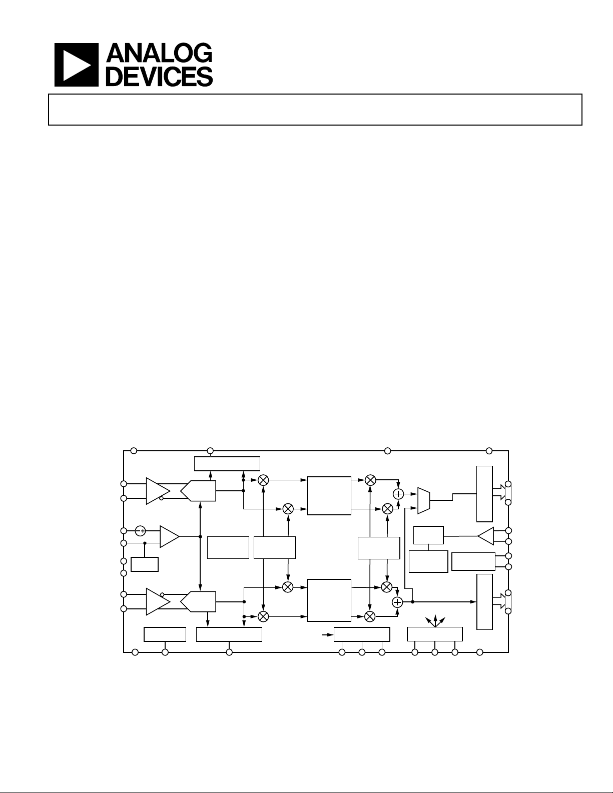
FUNCTIONAL BLOCK DIAGRAM
AVDD FD[0:3]
AD6655
APPLICATIONS
Communications
Diversity radio systems
Multimode digital receivers (3G)
TD-SCDMA, WiMax, WCDMA,
CDMA2000, GSM, EDGE, LTE
I/Q demodulation systems
Smart antenna systems
General-purpose software radios
Broadband data applications
PRODUCT HIGHLIGHTS
1. Integrated dual, 14-bit, 150 MSPS ADC.
2. Integrated wideband decimation filter and 32-bit
complex NCO.
3. Fast overrange detect and signal monitor with serial output.
4. Proprietary differential input maintains excellent SNR
performance for input frequencies up to 450 MHz.
5. Flexible output modes, including independent CMOS,
interleaved CMOS, IQ mode CMOS, and interleaved LVDS.
6. SYNC input allows synchronization of multiple devices.
7. 3-bit SPI port for register programming and register readback.
DVDD DRVDD
FD BITS/THRESHOLD
DETECT
VIN+A
VIN–A
VREF
ENSE
CML
RBIAS
VIN–B
VIN+B
NOTES
1.PIN NAMES ARE F OR THE CMOS PIN CONFI GURATION O NLY; SEE FIGURE 10 FO R LVDS PIN NAMES .
Rev. A
Information furnished by Analog Devices is believed to be accurate and reliable. However, no
responsibility is assumed by Analog Devices for its use, nor for any infringements of patents or other
rights of third parties that may result from its use. Specifications subject to change without notice. No
license is granted by implication or otherwise under any patent or patent rights of Analog Devices.
Trademarks and registered trademarks are the property of their respective owners.
SHA
REF
SELECT
SHA ADC
MULTI-CHIP
AGND
SYNC
SYNC FD[0:3]B SMI
ADC
SIGNAL
MONITOR
FD BITS/ THRESHOLD
DETECT
32-BIT
TUNING
NCO
SIGNAL MO NITOR
DATA
I
DECIMATING
HB FILTER +
Q
Q
DECIMATING
HB FILTER +
I
Figure 1.
AD6655
LP/HP
FIR
LP/HP
FIR
SIGNAL MONITOR
INTERFACE
SDFS
SMI
SCLK/
PDWN
f
ADC
NCO
/8
PROGRAMMING DAT A
SMI
SDO/
OEB
DIVIDE 1
TO 8
DUTY
CYCLE
STABILIZER
SDIO/
SCLK/
DCS
DFS
SPI
DCO
GENERATION
CSB DRGND
CMOS/LVDS
CMOS
D13A
D0A
OUTPUT BUFFER
CLK+
CLK–
DCOA
DCOB
D13B
D0B
OUTPUT BUFFER
06709-001
One Technology Way, P.O. Box 9106, Norwood, MA 02062-9106, U.S.A.
Tel: 781.329.4700 www.analog.com
Fax: 781.461.3113 ©2007–2009 Analog Devices, Inc. All rights reserved.

AD6655
TABLE OF CONTENTS
Features .............................................................................................. 1
Applications ....................................................................................... 1
Product Highlights ........................................................................... 1
Functional Block Diagram .............................................................. 1
Revision History ............................................................................... 3
General Description ......................................................................... 4
Specifications ..................................................................................... 5
ADC DC Specifications—AD6655BCPZ-80/
AD6655BCPZ-105 ......................................................................... 5
ADC DC Specifications—AD6655BCPZ-125/
AD6655BCPZ-150 ......................................................................... 6
ADC AC Specifications—AD6655BCPZ-80/
AD6655BCPZ-105 ......................................................................... 7
ADC AC Specifications—AD6655BCPZ-125/
AD6655BCPZ-150 ......................................................................... 8
Digital Specifications—AD6655BCPZ-80/AD6655BCPZ-105 .. 9
Digital Specifications—AD6655BCPZ-125/
AD6655BCPZ-150 ....................................................................... 11
Switching Specifications—AD6655BCPZ-80/
AD6655BCPZ-105 ....................................................................... 13
Switching Specifications—AD6655BCPZ-125/
AD6655BCPZ-150 ....................................................................... 14
Timing Specifications ................................................................ 15
Absolute Maximum Ratings .......................................................... 18
Thermal Characteristics ............................................................ 18
ESD Caution ................................................................................ 18
Pin Configurations and Function Descriptions ......................... 19
Equivalent Circuits ......................................................................... 23
Typical Performance Characteristics ........................................... 24
Theory of Operation ...................................................................... 29
ADC Architecture ...................................................................... 29
Analog Input Considerations .................................................... 29
Voltage Reference ....................................................................... 31
Clock Input Considerations ...................................................... 32
Power Dissipation and Standby Mode ..................................... 34
Digital Outputs ........................................................................... 35
Digital Downconverter .................................................................. 37
Downconverter Modes .............................................................. 37
Numerically Controlled Oscillator (NCO) ............................. 37
Half-Band Decimating Filter and FIR Filter ........................... 37
f
/8 Fixed-Frequency NCO ................................................... 37
ADC
Numerically Controlled Oscillator (NCO) ................................. 38
Frequency Translation ............................................................... 38
NCO Synchronization ............................................................... 38
Phase Offset................................................................................. 38
NCO Amplitude and Phase Dither .......................................... 38
Decimating Half-Band Filter and FIR filter ................................ 39
Half-Band Filter Coefficients .................................................... 39
Half-Band Filter Features .......................................................... 39
Fixed-Coefficient FIR Filter ...................................................... 39
Synchronization .......................................................................... 40
Combined Filter Performance .................................................. 40
Final NCO ................................................................................... 40
ADC Overrange and Gain Control .............................................. 41
Fast Detect Overview ................................................................. 41
ADC Fast Magnitude ................................................................. 41
ADC Overrange (OR) ................................................................ 42
Gain Switching ............................................................................ 42
Signal Monitor ................................................................................ 44
Peak Detector Mode................................................................... 44
RMS/MS Magnitude Mode ....................................................... 44
Threshold Crossing Mode ......................................................... 45
Additional Control Bits ............................................................. 45
DC Correction ............................................................................ 45
Signal Monitor SPORT Output ................................................ 46
Channel/Chip Synchronization .................................................... 47
Serial Port Interface (SPI) .............................................................. 48
Configuration Using the SPI ..................................................... 48
Hardware Interface ..................................................................... 48
Configuration Without the SPI ................................................ 49
SPI Accessible Features .............................................................. 49
Memory Map .................................................................................. 50
Reading the Memory Map Register Table ............................... 50
Memory Map Register Table ..................................................... 51
Memory Map Register Description ......................................... 55
Applications Information .............................................................. 59
Design Guidelines ...................................................................... 59
Evaluation Board ............................................................................ 61
Power Supplies ............................................................................ 61
Input Signals................................................................................ 61
Rev. A | Page 2 of 88

AD6655
Output Signals ............................................................................. 61
Default Operation and Jumper Selection Settings .................. 62
Alternative Clock Configurations ............................................. 62
Alternative Analog Input Drive Configuration ...................... 63
Schematics .................................................................................... 64
REVISION HISTORY
9/09—Rev. 0 to Rev. A
Added Exposed Pad Notation to Figure 9 and Table 12 ............ 19
Added Exposed Pad Notation to Figure 10 and Table 13 .......... 21
Updated Outline Dimensions ........................................................ 84
Changes to Ordering Guide ........................................................... 85
11/07—Revision 0: Initial Version
Evaluation Board Layouts .......................................................... 74
Bill of Materials ........................................................................... 82
Outline Dimensions ........................................................................ 84
Ordering Guide ........................................................................... 85
Rev. A | Page 3 of 8

AD6655
GENERAL DESCRIPTION
The AD6655 is a mixed-signal intermediate frequency (IF) receiver
consisting of dual 14-bit, 80 MSPS/105 MSPS/125 MSPS/150 MSPS
ADCs and a wideband digital downconverter (DDC). The AD6655
is designed to support communications applications where low
cost, small size, and versatility are desired.
The dual ADC core features a multistage, differential pipelined
architecture with integrated output error correction logic. Each
ADC features wide bandwidth differential sample-and-hold
analog input amplifiers supporting a variety of user-selectable
input ranges. An integrated voltage reference eases design considerations. A duty cycle stabilizer is provided to compensate for
variations in the ADC clock duty cycle, allowing the converters
to maintain excellent performance.
ADC data outputs are internally connected directly to the digital
downconverter (DDC) of the receiver, simplifying layout and
reducing interconnection parasitics. The digital receiver has two
channels and provides processing flexibility. Each receive channel
has four cascaded signal processing stages: a 32-bit frequency
translator (numerically controlled oscillator (NCO)), a halfband decimating filter, a fixed FIR filter, and an f
/8 fixed-
ADC
frequency NCO.
In addition to the receiver DDC, the AD6655 has several
functions that simplify the automatic gain control (AGC)
function in the system receiver. The fast detect feature allows
fast overrange detection by outputting four bits of input level
information with short latency.
In addition, the programmable threshold detector allows
monitoring of the incoming signal power using the four fast
detect bits of the ADC with low latency. If the input signal level
exceeds the programmable threshold, the coarse upper threshold
indicator goes high. Because this threshold indicator has low
latency, the user can quickly turn down the system gain to avoid
an overrange condition.
The second AGC-related function is the signal monitor. This
block allows the user to monitor the composite magnitude of the
incoming signal, which aids in setting the gain to optimize the
dynamic range of the overall system.
After digital processing, data can be routed directly to the two
external 14-bit output ports. These outputs can be set from 1.8 V
to 3.3 V CMOS or as 1.8 V LVDS. The CMOS data can also be
output in an interleaved configuration at a double data rate using
only Port A.
The AD6655 receiver digitizes a wide spectrum of IF frequencies.
Each receiver is designed for simultaneous reception of the main
channel and the diversity channel. This IF sampling architecture
greatly reduces component cost and complexity compared with
traditional analog techniques or less integrated digital methods.
Flexible power-down options allow significant power savings,
when desired.
Programming for setup and control is accomplished using a 3-bit
SPI-compatible serial interface.
The AD6655 is available in a 64-lead LFCSP and is specified over
the industrial temperature range of −40°C to +85°C.
Rev. A | Page 4 of 8

AD6655
SPECIFICATIONS
ADC DC SPECIFICATIONS—AD6655BCPZ-80/AD6655BCPZ-105
AVDD = 1.8 V, DVDD = 1.8 V, DRVDD = 1.8 V, maximum sample rate, VIN = −1.0 dBFS differential input, 1.0 V internal reference,
DCS enabled, unless otherwise noted.
Table 1.
AD6655BCPZ-80 AD6655BCPZ-105
Parameter
RESOLUTION Full 14 14 Bits
ACCURACY
No Missing Codes Full Guaranteed Guaranteed
Offset Error Full ±0.2 ±0.6 ±0.2 ±0.6 % FSR
Gain Error Full −3.6 −1.8 −0.1 −4.3 −2.2 −0.5 % FSR
MATCHING CHARACTERISTIC
Offset Error 25°C ±0.2 ±0.6 ±0.2 ±0.6 % FSR
Gain Error 25°C ±0.2 ±0.75 ±0.2 ±0.75 % FSR
TEMPERATURE DRIFT
Offset Error Full ±15 ±15 ppm/°C
Gain Error Full ±95 ±95 ppm/°C
INTERNAL VOLTAGE REFERENCE
Output Voltage Error (1 V Mode) Full ±5 ±18 ±5 ±18 mV
Load Regulation @ 1.0 mA Full 7 7 mV
INPUT-REFERRED NOISE
VREF = 1.0 V 25°C 0.85 0.85 LSB rms
ANALOG INPUT
Input Span, VREF = 1.0 V Full
Input Capacitance
1
Full
VREF INPUT RESISTANCE Full
POWER SUPPLIES
Supply Voltage
AVDD, DVDD Full
DRVDD (CMOS Mode) Full
DRVDD (LVDS Mode) Full
Supply Current
2, 3
I
AVDD
2, 3
I
DVDD
2
I
(3.3 V CMOS) Full
DRVDD
2
I
(1.8 V CMOS) Full
DRVDD
2
I
(1.8 V LVDS) Full
DRVDD
Full
Full
POWER CONSUMPTION
DC Input Full
Sine Wave Input2 (DRVDD = 1.8 V) Full
Sine Wave Input2 (DRVDD = 3.3 V) Full
Standby Power
4
Full
Power-Down Power Full
1
Input capacitance refers to the effective capacitance between one differential input pin and AGND. See for the equivalent analog input structure. Figure 11
2
Measured with a 9.7 MHz, full-scale sine wave input, NCO enabled with a frequency of 13 MHz, FIR filter enabled and the fS/8 output mix enabled with approximately
5 pF loading on each output bit.
3
The maximum limit applies to the combination of I
4
Standby power is measured with a dc input and with the CLK pin inactive (set to AVDD or AGND).
AVDD
and I
2 2
8 8
6 6
1.7 1.8 1.9 1.7 1.8 1.9
1.7 3.3 3.6 1.7 3.3 3.6
1.7 1.8 1.9 1.7 1.8 1.9
235
175 225
420
315
575
18 21
8 11
55 56
470 490 620 650
755 995
800 1040
52 68
2.5 8 2.5 8
currents.
DVDD
Unit Temperature Min Typ Max Min Typ Max
V p-p
pF
kΩ
V
V
V
mA
mA
mA
mA
mA
mW
mW
mW
mW
mW
Rev. A | Page 5 of 8

AD6655
ADC DC SPECIFICATIONS—AD6655BCPZ-125/AD6655BCPZ-150
AVDD = 1.8 V, DVDD = 1.8 V, DRVDD = 1.8 V, maximum sample rate, VIN = −1.0 dBFS differential input, 1.0 V internal reference,
DCS enabled, unless otherwise noted.
Table 2.
AD6655BCPZ-125 AD6655BCPZ-150
Parameter Temperature
RESOLUTION Full 14 14 Bits
ACCURACY
No Missing Codes Full Guaranteed Guaranteed
Offset Error Full ±0.3 ±0.6 ±0.2 ±0.6 % FSR
Gain Error Full −4.7 −2.7 −0.8 −5.1 −3.2 −1.0 % FSR
MATCHING CHARACTERISTIC
Offset Error 25°C ±0.3 ±0.7 ±0.2 ±0.7 % FSR
Gain Error 25°C ±0.1 ±0.7 ±0.2 ±0.8 % FSR
TEMPERATURE DRIFT
Offset Error Full ±15 ±15 ppm/°C
Gain Error Full ±95 ±95 ppm/°C
INTERNAL VOLTAGE REFERENCE
Output Voltage Error (1 V Mode) Full ±5 ±18 ±5 ±18 mV
Load Regulation @ 1.0 mA Full 7 7 mV
INPUT-REFERRED NOISE
VREF = 1.0 V 25°C 0.85 0.85 LSB rms
ANALOG INPUT
Input Span, VREF = 1.0 V Full 2 2 V p-p
Input Capacitance
1
Full 8 8 pF
VREF INPUT RESISTANCE Full 6 6 kΩ
POWER SUPPLIES
Supply Voltage
AVDD, DVDD Full 1.7 1.8 1.9 1.7 1.8 1.9 V
DRVDD (CMOS Mode) Full 1.7 1.8 3.6 1.7 1.8 3.6 V
DRVDD (LVDS Mode) Full 1.7 1.8 1.9 1.7 1.8 1.9 V
Supply Current
2, 3
I
Full 390
AVDD
2, 3
I
DVDD
2
I
(3.3 V CMOS) Full 26 28 mA
DRVDD
2
I
(1.8 V CMOS) Full 13 17 mA
DRVDD
2
I
(1.8 V LVDS) Full 57 57 mA
DRVDD
Full 270 320 mA
705
440
805
POWER CONSUMPTION
DC Input Full 770 810 870 920 mW
Sine Wave Input2 (DRVDD = 1.8 V) Full 1215 1395 mW
Sine Wave Input2 (DRVDD = 3.3 V) Full 1275 1450 mW
Standby Power
4
Full 77 77 mW
Power-down Power Full 2.5 8 2.5 8 mW
1
Input capacitance refers to the effective capacitance between one differential input pin and AGND. See for the equivalent analog input structure. Figure 11
2
Measured with a 9.7 MHz, full-scale sine wave input, NCO enabled with a frequency of 13 MHz, FIR filter enabled and the fS/8 output mix enabled with approximately
5 pF loading on each output bit.
3
The maximum limit applies to the combination of I
4
Standby power is measured with a dc input, the CLK pin inactive (set to AVDD or AGND).
AVDD
and I
DVDD
currents.
Unit Min Typ Max Min Typ Max
mA
Rev. A | Page 6 of 8

AD6655
ADC AC SPECIFICATIONS—AD6655BCPZ-80/AD6655BCPZ-105
AVDD = 1.8 V, DVDD = 1.8 V, DRVDD = 1.8 V, maximum sample rate, VIN = −1.0 dBFS differential input, 1.0 V internal reference,
DCS enabled, NCO enabled, half-band filter enabled, FIR filter enabled, unless otherwise noted.
Table 3.
1
Parameter
Te mp e ra tu r e
SIGNAL-TO-NOISE-RATIO (SNR)
fIN = 2.4 MHz 25°C 74.9 74.8 dB
fIN = 70 MHz 25°C 74.8 74.7 dB
Full 73.0 73.0 dB
fIN = 140 MHz 25°C 74.5 74.3 dB
fIN = 220 MHz 25°C
WORST SECOND OR THIRD HARMONIC
fIN = 2.4 MHz
fIN = 70 MHz
fIN = 140 MHz
fIN = 220 MHz
SPURIOUS-FREE DYNAMIC RANGE
25°C
25°C
Full
25°C
25°C
(SFDR)
fIN = 2.4 MHz
fIN = 70 MHz
fIN = 140 MHz
fIN = 220 MHz
WORST OTHER HARMONIC OR SPUR
2
fIN = 2.4 MHz
fIN = 70 MHz
fIN = 140 MHz
fIN = 220 MHz
TWO-TONE SFDR
fIN = 29.12 MHz, 32.12 MHz (−7 dBFS)
fIN = 169.12 MHz, 172.12 MHz (−7 dBFS)
CROSSTALK
3
ANALOG INPUT BANDWIDTH
1
See Application Note AN-835, Understanding High Speed ADC Testing and Evaluation, for a complete set of definitions.
2
See the section for more information about the worst other specifications for the AD6655. Applications Information
3
Crosstalk is measured at 100 MHz with −1 dBFS on one channel and with no input on the alternate channel.
25°C
25°C
Full 74
25°C
25°C
25°C
25°C
Full
25°C
25°C
25°C
25°C
Full
25°C
AD6655BCPZ-80 AD6655BCPZ-105
Unit Min Typ Max Min Typ Max
73.4 73.4
−86 −86
−85 −85
−74
−74
−84 −84
−83 −83
dB
dBc
dBc
dBc
dBc
dBc
86 86
85 85
74
84 84
83 83
dBc
dBc
dBc
dBc
dBc
−93 −93
−90 −90
−82
−82
−89 −89
−86 −86
dBc
dBc
dBc
dBc
dBc
85 85
81 81
95 95
650 650
dBc
dBc
dB
MHz
Rev. A | Page 7 of 8

AD6655
ADC AC SPECIFICATIONS—AD6655BCPZ-125/AD6655BCPZ-150
AVDD = 1.8 V, DVDD = 1.8 V, DRVDD = 1.8 V, maximum sample rate, VIN = −1.0 dBFS differential input, 1.0 V internal reference,
DCS enabled, NCO enabled, half-band filter enabled, FIR filter enabled, unless otherwise noted.
Table 4.
1
Parameter
Te mp e ra tu r e
SIGNAL-TO-NOISE-RATIO (SNR)
fIN = 2.4 MHz 25°C 74.7 74.6 dB
fIN = 70 MHz 25°C 74.6 74.5 dB
Full 73.0
fIN = 140 MHz 25°C 74.2 73.9 dB
fIN = 220 MHz 25°C
WORST SECOND OR THIRD HARMONIC
fIN = 2.4 MHz
fIN = 70 MHz
fIN = 140 MHz
fIN = 220 MHz
SPURIOUS-FREE DYNAMIC RANGE (SFDR)
fIN = 2.4 MHz
fIN = 70 MHz
fIN = 140 MHz
fIN = 220 MHz
WORST OTHER HARMONIC OR SPUR
2
fIN = 2.4 MHz
fIN = 70 MHz
fIN = 140 MHz
fIN = 220 MHz
TWO-TONE SFDR
fIN = 29.12 MHz, 32.12 MHz (−7 dBFS)
fIN = 169.12 MHz, 172.12 MHz (−7 dBFS)
CROSSTALK
3
ANALOG INPUT BANDWIDTH
1
See Application Note AN-835, Understanding High Speed ADC Testing and Evaluation, for a complete set of definitions.
2
See the section for more information about the worst other specifications for the AD6655. Applications Information
3
Crosstalk is measured at 100 MHz with −1 dBFS on one channel and with no input on the alternate channel.
25°C
25°C
Full
25°C
25°C
25°C
25°C
Full
25°C
25°C
25°C
25°C
Full
25°C
25°C
25°C
25°C
Full
25°C
AD6655BCPZ-125 AD6655BCPZ-150
Unit Min Typ Max Min Typ Max
73.3
72.5
73.0
−86 −85
−85 −84
−73
−84 −83
−83 −77
86 85
85 80
73
73
84 76
83 74
−92 −87
−90 −80
−82 −80
−88 −76
−84 −74
85 85
81 81
95 95
650 650
dB
dB
dBc
dBc
−73 dBc
dBc
dBc
dBc
dBc
dBc
dBc
dBc
dBc
dBc
dBc
dBc
dBc
dBc
dBc
dB
MHz
Rev. A | Page 8 of 88

AD6655
DIGITAL SPECIFICATIONS—AD6655BCPZ-80/AD6655BCPZ-105
AVDD = 1.8 V, DVDD = 1.8 V, DRVDD = 1.8 V, maximum sample rate, VIN = −1.0 dBFS differential input, 1.0 V internal reference,
DCS enabled, unless otherwise noted.
Table 5.
AD6655BCPZ-80 AD6655BCPZ-105
Parameter Temp
DIFFERENTIAL CLOCK INPUTS (CLK+, CLK−)
Logic Compliance
Internal Common-Mode Bias
Differential Input Voltage
Input Voltage Range
Input Common-Mode Range
CMOS/LVDS/LVPECL CMOS/LVDS/LVPECL
Full 1.2 1.2 V
Full 0.2 6 0.2 6
Full AVDD
− 0.3 AVDD + 1.6 AVDD − 0.3 AVDD + 1.6
Full 1.1 AVDD 1.1 AVDD
High Level Input Voltage Full 1.2 3.6 1.2 3.6 V
Low Level Input Voltage Full
High Level Input Current Full
Low Level Input Current Full
Input Capacitance
Input Resistance
Full 4 4
Full 8 10 12 8 10 12
00.80 0.8
−10 +10 −10 +10
−10 +10 −10 +10
SYNC INPUT
Logic Compliance CMOS CMOS
Internal Bias Full 1.2 1.2 V
Input Voltage Range Full AVDD − 0.3 AVDD + 1.6 AVDD − 0.3 AVDD + 1.6 V
High Level Input Voltage Full 1.2 3.6 1.2 3.6 V
Low Level Input Voltage Full 0 0.8 0 0.8 V
High Level Input Current Full −10 +10 −10 +10 μA
Low Level Input Current Full −10 +10 −10 +10 μA
Input Capacitance Full 4 4 pF
Input Resistance Full 8 10 12 8 10 12 kΩ
LOGIC INPUT (CSB)
1
High Level Input Voltage Full 1.22 3.6 1.22 3.6 V
Low Level Input Voltage Full
High Level Input Current Full
Low Level Input Current Full
Input Resistance Full
Input Capacitance Full
LOGIC INPUT (SCLK/DFS)
2
00.60 0.6
−10 +10 −10 +10
40 132 40 132
26 26
22
High Level Input Voltage Full 1.22 3.6 1.22 3.6 V
Low Level Input Voltage Full
High Level Input Current Full
Low Level Input Current Full
Input Resistance Full
Input Capacitance Full
LOGIC INPUTS (SDIO/DCS, SMI SDFS)
1
High Level Input Voltage Full
Low Level Input Voltage Full
High Level Input Current Full
Low Level Input Current Full
Input Resistance Full
Input Capacitance Full
00.60 0.6
−92 −135 −92 −135
−10 +10 −10 +10
26 26
22
1.22 3.6 1.22 3.6
00.60 0.6
−10 +10 −10 +10
38 128 38 128
26 26
55
Unit Min Typ Max Min Typ Max
V p-p
V
V
V
μA
μA
pF
kΩ
V
μA
μA
kΩ
pF
V
μA
μA
kΩ
pF
V
V
μA
μA
kΩ
pF
Rev. A | Page 9 of 88

AD6655
AD6655BCPZ-80 AD6655BCPZ-105
Parameter Temp
LOGIC INPUTS (SMI SDO/OEB,
SMI SCLK/PDWN)
2
High Level Input Voltage Full
Low Level Input Voltage Full
High Level Input Current Full
Low Level Input Current Full
Input Resistance Full
Input Capacitance Full
DIGITAL OUTPUTS
1.22 3.6 1.22 3.6
00.60 0.6
−90 −134 −90 −134
−10 +10 −10 +10
26 26
55
CMOS Mode—DRVDD = 3.3 V
High Level Output Voltage
IOH = 50 μA Full
IOH = 0.5 mA Full
3.29 3.29
3.25 3.25
Low Level Output Voltage
IOL = 1.6 mA Full
IOL = 50 μA Full
0.2 0.2
0.05 0.05
CMOS Mode—DRVDD = 1.8 V
High Level Output Voltage
IOH = 50 μA Full
IOH = 0.5 mA Full
1.79 1.79
1.75 1.75
Low Level Output Voltage
IOL = 1.6 mA Full
IOL = 50 μA Full
0.2 0.2
0.05 0.05
LVDS Mode, DRVDD = 1.8 V
Differential Output Voltage (VOD),
Full
250 350 450 250 350 450
ANSI Mode
Output Offset Voltage (VOS),
Full
1.15 1.25 1.35 1.15 1.25 1.35
ANSI Mode
Differential Output Voltage (VOD),
Full
150 200 280 150 200 280
Reduced Swing Mode
Output Offset Voltage (VOS),
Full
1.15 1.25 1.35 1.15 1.25 1.35
Reduced Swing Mode
1
Pull up.
2
Pull down.
Unit Min Typ Max Min Typ Max
V
V
μA
μA
kΩ
pF
V
V
V
V
V
V
V
V
mV
V
mV
V
Rev. A | Page 10 of 88

AD6655
DIGITAL SPECIFICATIONS—AD6655BCPZ-125/AD6655BCPZ-150
AVDD = 1.8 V, DVDD = 1.8 V, DRVDD = 1.8 V, maximum sample rate, VIN = −1.0 dBFS differential input, 1.0 V internal reference,
DCS enabled, unless otherwise noted.
Table 6.
AD6655BCPZ-125 AD6655BCPZ-150
Parameter Temp
DIFFERENTIAL CLOCK INPUTS (CLK+, CLK−)
Logic Compliance
Internal Common-Mode Bias
Differential Input Voltage
Input Voltage Range
Input Common-Mode Range
CMOS/LVDS/LVPECL CMOS/LVDS/LVPECL
Full 1.2 1.2 V
Full 0.2 6 0.2
Full AVDD− 0.3 AVDD + 1.6 AVDD − 0.3
Full 1.1 V AVD D 1. 1 V
6
AVD D + 1 .6
AVD D
High Level Input Voltage Full 1.2 3.6 1.2 3.6 V
Low Level Input Voltage Full 0 0.8 0 0.8 V
High Level Input Current Full −10 +10 −10 +10 μA
Low Level Input Current Full −10 +10 −10 +10 μA
Input Capacitance
Input Resistance
Full 4 4
Full 8 10 12 8 10 12
SYNC INPUT
Logic Compliance CMOS CMOS
Internal Bias Full 1.2 1.2 V
Input Voltage Range Full AVDD − 0.3 AVDD + 1.6 AVDD − 0.3 AVDD + 1.6 V
High Level Input Voltage Full 1.2 3.6 1.2 3.6 V
Low Level Input Voltage Full 0 0.8 0 0.8 V
High Level Input Current Full −10 +10 −10 +10 μA
Low Level Input Current Full −10 +10 −10 +10 μA
Input Capacitance Full 4 4 pF
Input Resistance Full 8 10 12 8 10 12 kΩ
LOGIC INPUT (CSB)
1
High Level Input Voltage Full 1.22 3.6 1.22 3.6 V
Low Level Input Voltage Full 0 0.6 0 0.6 V
High Level Input Current Full −10 +10 −10 +10 μA
Low Level Input Current Full 40 132 40 132 μA
Input Resistance Full 26 26 kΩ
Input Capacitance Full 2 2 pF
LOGIC INPUT (SCLK/DFS)
2
High Level Input Voltage Full 1.22 3.6 1.22 3.6 V
Low Level Input Voltage Full 0 0.6 0 0.6 V
High Level Input Current Full −92 −135 −92 −135 μA
Low Level Input Current Full −10 +10 −10 +10 μA
Input Resistance Full 26 26 kΩ
Input Capacitance Full 2 2 pF
LOGIC INPUTS (SDIO/DCS, SMI SDFS)
1
High Level Input Voltage Full 1.22 3.6 1.22 3.6 V
Low Level Input Voltage Full 0 0.6 0 0.6 V
High Level Input Current Full −10 +10 −10 +10 μA
Low Level Input Current Full 38 128 38 128 μA
Input Resistance Full 26 26 kΩ
Input Capacitance Full 5 5 pF
Unit Min Typ Max Min Typ Max
V p-p
V
V
pF
kΩ
Rev. A | Page 11 of 88

AD6655
AD6655BCPZ-125 AD6655BCPZ-150
Parameter Temp
LOGIC INPUTS (SMI SDO/OEB,
SMI SCLK/PDWN)
2
High Level Input Voltage Full 1.22 3.6 1.22 3.6 V
Low Level Input Voltage Full 0 0.6 0 0.6 V
High Level Input Current Full −90 −134 −90 −134 μA
Low Level Input Current Full −10 +10 −10 +10 μA
Input Resistance Full 26 26 kΩ
Input Capacitance Full 5 5 pF
DIGITAL OUTPUTS
CMOS Mode—DRVDD = 3.3 V
High Level Output Voltage
IOH = 50 μA Full 3.29 3.29 V
IOH = 0.5 mA Full 3.25 3.25 V
Low Level Output Voltage
IOL = 1.6 mA Full 0.2 0.2 V
IOL = 50 μA Full 0.05 0.05 V
CMOS Mode—DRVDD = 1.8 V
High Level Output Voltage
IOH = 50 μA Full 1.79 1.79 V
IOH = 0.5 mA Full 1.75 1.75 V
Low Level Output Voltage
IOL = 1.6 mA Full 0.2 0.2 V
IOL = 50 μA Full 0.05 0.05 V
LVDS Mode—DRVDD = 1.8 V
Differential Output Voltage (VOD),
Full 250 350 450 250 350 450 mV
ANSI Mode
Output Offset Voltage (VOS),
Full 1.15 1.25 1.35 1.15 1.25 1.35 V
ANSI Mode
Differential Output Voltage (VOD),
Full 150 200 280 150 200 280 mV
Reduced Swing Mode
Output Offset Voltage (VOS),
Full 1.15 1.25 1.35 1.15 1.25 1.35 V
Reduced Swing Mode
1
Pull up.
2
Pull down.
Unit Min Typ Max Min Typ Max
Rev. A | Page 12 of 88

AD6655
SWITCHING SPECIFICATIONS—AD6655BCPZ-80/AD6655BCPZ-105
Table 7.
AD6655BCPZ-80 AD6655BCPZ-105
Parameter Temp
CLOCK INPUT PARAMETERS
Input Clock Rate Full 625 625 MHz
Conversion Rate
1
DCS Enabled Full 20 80 20 105 MSPS
DCS Disabled Full 10 80 10 105 MSPS
CLK Period—Divide-by-1 Mode (t
CLK Pulse Width High (t
)
CLKH
) Full 12.5 9.5 ns
CLK
Divide-by-1 Mode, DCS Enabled Full 3.75 6.25 8.75 2.85 4.75 6.65 ns
Divide-by-1 Mode DCS Disabled Full 5.63 6.25 6.88 4.28 4.75 5.23 ns
Divide-by-2 Mode, DCS Enabled Full 1.6 1.6 ns
Divide-by-3 Through Divide-by-8 Modes, DCS Enabled Full 0.8 0.8 ns
DATA OUTPUT PARAMETERS (DATA, FD)
CMOS Noninterleaved Mode—DRVDD = 1.8 V
Data Propagation Delay (tPD)
DCO Propagation Delay (t
2
Full 1.6 3.9 6.2 1.6 3.9 6.2 ns
) Full 4.0 5.4 7.3 4.0 5.4 7.3 ns
DCO
Setup Time (tS) Full 14.0 11.0 ns
Hold Time (tH) Full 11.0 8.0 ns
CMOS Noninterleaved Mode—DRVDD = 3.3 V
Data Propagation Delay (tPD)
DCO Propagation Delay (t
2
Full 1.9 4.1 6.4 1.9 4.1 6.4 ns
) Full 4.4 5.8 7.7 4.4 5.8 7.7 ns
DCO
Setup Time (tS) Full 14.2 11.2 ns
Hold Time (tH) Full 10.8 7.8 ns
CMOS Interleaved and IQ Mode—DRVDD = 1.8 V
Data Propagation Delay (tPD)
DCO Propagation Delay (t
2
Full 1.6 3.9 6.2 1.6 3.9 6.2 ns
) Full 3.4 4.8 6.7 3.4 4.8 6.7 ns
DCO
Setup Time (tS) Full 7.15 5.65 ns
Hold Time (tH) Full 5.35 3.85 ns
CMOS Interleaved and IQ Mode—DRVDD = 3.3 V
Data Propagation Delay (tPD)
DCO Propagation Delay (t
2
Full 1.9 4.1 6.4 1.9 4.1 6.4 ns
) Full 3.8 5.2 7.1 3.8 5.2 7.1 ns
DCO
Setup Time (tS) Full 7.35 5.85 ns
Hold Time (tH) Full 5.15 3.65 ns
LVDS Mode—DRVDD = 1.8 V
Data Propagation Delay (tPD)
DCO Propagation Delay (t
2
Full 2.5 4.8 7.0 2.5 4.8 7.0 ns
) Full 3.7 5.3 7.3 3.7 5.3 7.3 ns
DCO
Pipeline Delay (Latency) NCO, FIR, fS/8 Mix Disabled Full 38 38 Cycles
Pipeline Delay (Latency) NCO Enabled, FIR and fS/8 Mix Disabled
Full 38 38 Cycles
(Complex Output Mode)
Pipeline Delay (Latency) NCO, FIR, and fS/8 Mix Enabled Full 109 109 Cycles
Aperture Delay (tA) Full 1.0 1.0 ns
Aperture Uncertainty (Jitter, tJ) Full 0.1 0.1 ps rms
Wake-Up Time
3
Full 350 350 us
OUT-OF-RANGE RECOVERY TIME Full 2 2 Cycles
1
Conversion rate is the clock rate after the divider.
2
Output propagation delay is measured from CLK 50% transition to DATA 50% transition, with a 5 pF load.
3
Wake-up time is dependent on the value of the decoupling capacitors.
Unit Min Typ Max Min Typ Max
Rev. A | Page 13 of 88

AD6655
SWITCHING SPECIFICATIONS—AD6655BCPZ-125/AD6655BCPZ-150
Table 8.
AD6655BCPZ-125 AD6655BCPZ-150
Parameter Temp
CLOCK INPUT PARAMETERS
Input Clock Rate Full 625 625 MHz
Conversion Rate
1
DCS Enabled Full 20 125 20 150 MSPS
DCS Disabled Full 10 125 10 150 MSPS
CLK Period—Divide-by-1 Mode (t
CLK Pulse Width High (t
)
CLKH
) Full 8 6.66 ns
CLK
Divide-by-1 Mode, DCS Enabled Full 2.4 4 5.6 2.0 3.33 4.66 ns
Divide-by-1 Mode, DCS Disabled Full 3.6 4 4.4 3.0 3.33 3.66 ns
Divide-by-2 Mode, DCS Enabled Full 1.6 1.6 ns
Divide-by-3 Through Divide-by-8 Modes, DCS Enabled Full 0.8 0.8 ns
DATA OUTPUT PARAMETERS (DATA, FD)
CMOS Noninterleaved Mode—DRVDD = 1.8 V
Data Propagation Delay (tPD)
DCO Propagation Delay (t
2
Full 1.6 3.9 6.2 1.6 3.9 6.2 ns
) Full 4.0 5.4 7.3 4.0 5.4 7.3 ns
DCO
Setup Time (tS) Full 9.5 8.16 ns
Hold Time (tH) Full 6.5 5.16 ns
CMOS Noninterleaved Mode—DRVDD = 3.3 V
Data Propagation Delay (tPD)
DCO Propagation Delay (t
2
Full 1.9 4.1 6.4 1.9 4.1 6.4 ns
) Full 4.4 5.8 7.7 4.4 5.8 7.7 ns
DCO
Setup Time (tS) Full 9.7 8.36 ns
Hold Time (tH) Full 6.3 4.96 ns
CMOS Interleaved and IQ Mode—DRVDD = 1.8 V
Data Propagation Delay (tPD)
DCO Propagation Delay (t
2
Full 1.6 3.9 6.2 1.6 3.9 6.2 ns
) Full 3.4 4.8 6.7 3.4 4.8 6.7 ns
DCO
Setup Time (tS) Full 4.9 4.23 ns
Hold Time (tH) Full 3.1 2.43 ns
CMOS Interleaved and IQ Mode—DRVDD = 3.3 V
Data Propagation Delay (tPD)
DCO Propagation Delay (t
2
Full 1.9 4.1 6.4 1.9 4.1 6.4 ns
) Full 3.8 5.2 7.1 3.8 5.2 7.1 ns
DCO
Setup Time (tS) Full 5.1 4.43 ns
Hold Time (tH) Full 2.9 2.23 ns
LVDS Mode—DRVDD = 1.8 V
Data Propagation Delay (tPD)
DCO Propagation Delay (t
2
Full 2.5 4.8 7.0 2.5 4.8 7.0 ns
) Full 3.7 5.3 7.3 3.7 5.3 7.3 ns
DCO
Pipeline Delay (Latency) NCO, FIR, fS/8 Mix Disabled Full 38 38 Cycles
Pipeline Delay (Latency) NCO Enabled; FIR and fS/8 Mix Disabled
Full 38 38 Cycles
(Complex Output Mode)
Pipeline Delay (Latency) NCO, FIR, and fS/8 Mix Enabled Full 109 109 Cycles
Aperture Delay (tA) Full 1.0 1.0 ns
Aperture Uncertainty (Jitter, tJ) Full 0.1 0.1 ps rms
Wake-Up Time
3
Full 350 350 us
OUT-OF-RANGE RECOVERY TIME Full 3 3 Cycles
1
Conversion rate is the clock rate after the divider.
2
Output propagation delay is measured from CLK 50% transition to DATA 50% transition, with a 5 pF load.
3
Wake-up time is dependent on the value of the decoupling capacitors.
Unit Min Typ Max Min Typ Max
Rev. A | Page 14 of 88
AD6655
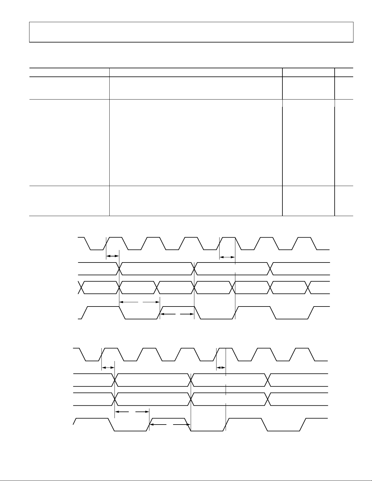
TIMING SPECIFICATIONS
Table 9.
Parameter Conditions Min Typ Max Unit
SYNC TIMING REQUIREMENTS
t
SYNC to the rising edge of CLK setup time 0.24 ns
SSYNC
t
SYNC to the rising edge of CLK hold time 0.4 ns
HSYNC
SPI TIMING REQUIREMENTS
tDS Setup time between the data and the rising edge of SCLK 2 ns
tDH Hold time between the data and the rising edge of SCLK 2 ns
t
Period of the SCLK 40 ns
CLK
tS Setup time between CSB and SCLK 2 ns
tH Hold time between CSB and SCLK 2 ns
t
Minimum period that SCLK should be in a logic high state 10 ns
HIGH
t
Minimum period that SCLK should be in a logic low state 10 ns
LOW
t
EN_SDIO
Time required for the SDIO pin to switch from an input to an output
relative to the SCLK falling edge
t
DIS_SDIO
Time required for the SDIO pin to switch from an output to an input
relative to the SCLK rising edge
SPORT TIMING REQUIREMENTS
t
Delay from rising edge of CLK+ to rising edge of SMI SCLK 3.2 4.5 6.2 ns
CSSCLK
t
Delay from rising edge of SMI SCLK to SMI SDO −0.4 0 +0.4 ns
SSLKSDO
t
Delay from rising edge of SMI SCLK to SMI SDFS −0.4 0 +0.4 ns
SSCLKSDFS
10 ns
10 ns
Timing Diagrams
CLK+
t
DCO
CHANNEL A/B
DATA BITS
CHANNEL A/B
FD BITS
CHANNEL A/B
CHANNEL A/B
FD BITS
DATA BITS
06709-109
DECIMATED
CMOS DATA
DECIMATED
FD DATA
DECIMATED
DCOA/DCOB
CHANNEL A/B
FD BITS
t
PD
CHANNEL A/B
FD BITS
t
S
CHANNEL A/B
DATA BITS
CHANNEL A/B
FD BITS
t
CHANNEL A/B
FD BITS
H
Figure 2. Decimated Noninterleaved CMOS Mode Data and Fast Detect Output Timing (Fast Detect Mode Select Bits = 000)
CLK+
t
PD
DECIMATED
CMOS DATA
DECIMATED
FD DATA
DECIMATED
DCOA/DCOB
CHANNEL A/B
CHANNEL A/B
t
S
DATA BITS
FD BITS
t
H
Figure 3. Decimated Noninterleav ed CMOS Mode Data and Fast Detect Output Ti ming (Fast Detect Mode Select Bits = 001 Th rough Fast Detect Mode Select Bits = 100)
t
DCO
CHANNEL A/B
DATA BITS
CHANNEL A/B
FD BITS
CHANNEL A/B
DATA BITS
CHANNEL A/B
FD BITS
06709-012
Rev. A | Page 15 of 88
AD6655
CLK+
t
PD
t
DCO
OUTPUT DATA
DECIMATED
INTERLEAVED
CMOS DATA
DECIMATED
INTERLEAVED
FD DATA
DECIMATED
DCO
CLK+
DECIMATED
CMOS IQ
CMOS FD
DATA
DECIMATED
DCOA/DCOB
CLK–
CHANNEL A:
DATA
CHANNEL A:
FD BITS
CHANNEL A/B:
Q DATA
CHANNEL A/B:
FD BITS
CHANNEL B:
DATA
CHANNEL B:
FD BITS
CHANNEL A:
DATA
CHANNEL A:
FD BITS
t
S
CHANNEL B:
DATA
CHANNEL B:
FD BITS
t
H
CHANNEL A:
DATA
CHANNEL A:
FD BITS
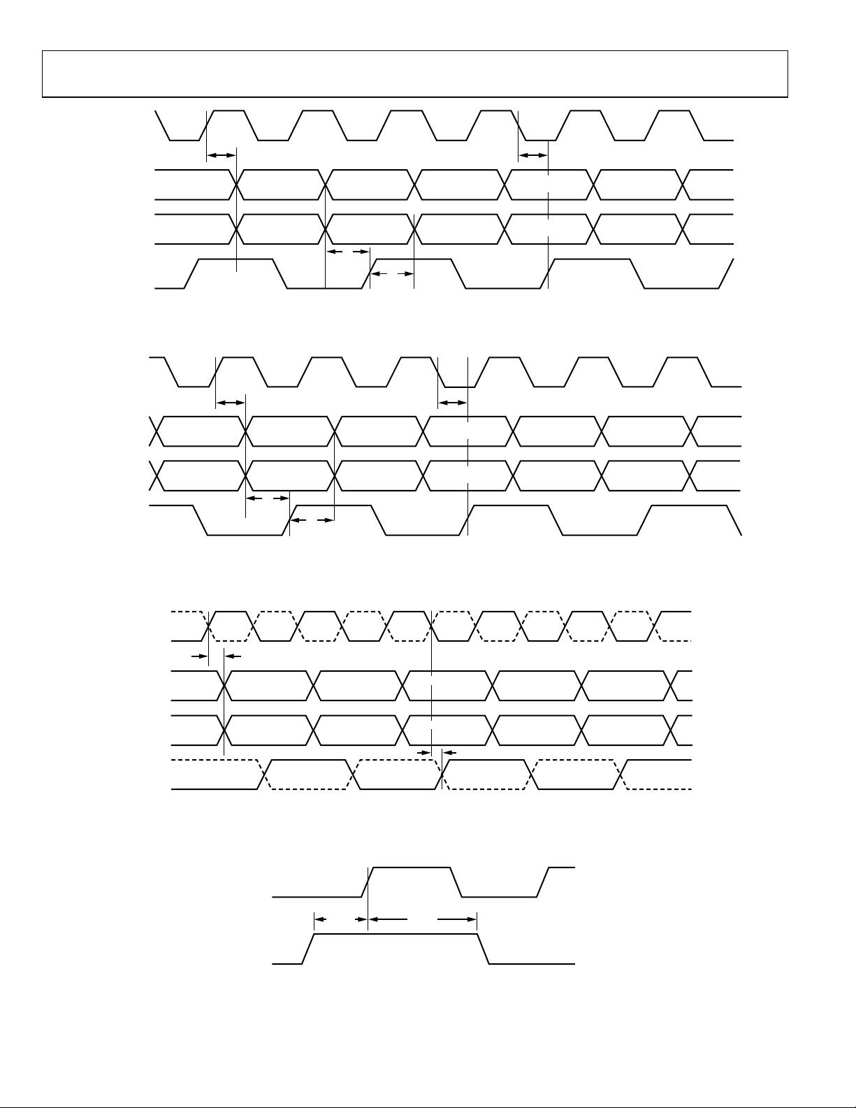
Figure 4. Decimated Interleaved CMOS Mode Data and Fast Detect Output Timing
t
PD
CHANNEL A/B:
I DATA
CHANNEL A/B:
FD BITS
t
S
t
H
CHANNEL A/B:
Q DATA
CHANNEL A/B:
FD BITS
t
DCO
CHANNEL A/B:
I DATA
CHANNEL A/B:
FD BITS
CHANNEL A/B:
Q DATA
CHANNEL A/B:
FD BITS
Figure 5. Decimated IQ Mode CMOS Data and Fast Detect Output Timing
CHANNEL B:
DATA
CHANNEL B:
FD BITS
CHANNEL A/B:
I DATA
CHANNEL A/B:
FD BITS
06709-013
06709-014
CLK+
LVDS
DATA
LVDS
FAST DET
DCO–
DCO+
t
PD
CHANNEL A:
DATA
CHANNEL A:
FD
CHANNEL B:
DATA
CHANNEL B:
FD
CHANNEL A:
DATA
CHANNEL A:
FD
t
DCO
CHANNEL B:
DATA
CHANNEL B:
FD
CHANNEL A:
DATA
CHANNEL A:
FD
06709-015
Figure 6. Decimated Interleaved LVDS Mode Data and Fast Detect Output Timing
CLK+
SYNC
t
SSYNC
t
HSYNC
06709-016
Figure 7. SYNC Timing Inputs
Rev. A | Page 16 of 88
AD6655
CLK+
CLK–
SMI SCLK
SMI SDFS
I SDO
SM
t
CSSCLK
t
SSCLKSDFS
t
SSCLKSDFS
DATA DATA
06709-017
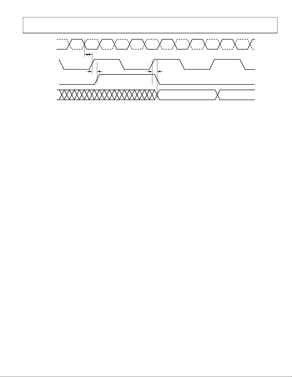
Figure 8. Signal Monitor SPORT Output Timing
Rev. A | Page 17 of 88
AD6655
ABSOLUTE MAXIMUM RATINGS
Table 10.
Parameter Rating
ELECTRICAL
AVDD, DVDD to AGND −0.3 V to +2.0 V
DRVDD to DRGND −0.3 V to +3.9 V
AGND to DRGND −0.3 V to +0.3 V
VIN+A/VIN+B, VIN-A/VIN−B to AGND −0.3 V to AVDD + 0.2 V
CLK+, CLK− to AGND −0.3 V to +3.9 V
SYNC to AGND −0.3 V to +3.9 V
VREF to AGND −0.3 V to AVDD + 0.2 V
SENSE to AGND −0.3 V to AVDD + 0.2 V
CML to AGND −0.3 V to AVDD + 0.2 V
RBIAS to AGND −0.3 V to AVDD + 0.2 V
CSB to AGND −0.3 V to +3.9 V
SCLK/DFS to DRGND −0.3 V to +3.9 V
SDIO/DCS to DRGND −0.3 V to DRVDD + 0.3 V
SMI SDO/OEB to DRGND −0.3 V to DRVDD + 0.3 V
SMI SCLK/PDWN to DRGND −0.3 V to DRVDD + 0.3 V
SMI SDFS to DRGND −0.3 V to DRVDD + 0.3 V
D0A/D0B through D13A/D13B
−0.3 V to DRVDD + 0.3 V
to DRGND
FD0A/FD0B through FD3A/FD3B to
−0.3 V to DRVDD + 0.3 V
DRGND
DCOA/DCOB to DRGND −0.3 V to DRVDD + 0.3 V
ENVIRONMENTAL
Operating Temperature Range
−40°C to +85°C
(Ambient)
Maximum Junction Temperature
150°C
Under Bias
Storage Temperature Range
−65°C to +125°C
(Ambient)
Stresses above those listed under Absolute Maximum Ratings
may cause permanent damage to the device. This is a stress
rating only; functional operation of the device at these or any
other conditions above those indicated in the operational
section of this specification is not implied. Exposure to absolute
maximum rating conditions for extended periods may affect
device reliability.
THERMAL CHARACTERISTICS
The exposed paddle must be soldered to the ground plane for
the LFCSP package. Soldering the exposed paddle to the
customer board increases the reliability of the solder joints,
maximizing the thermal capability of the package.
Table 11. Thermal Resistance
Airflow
Package
Typ e
64-Lead LFCSP
9 mm × 9 mm
(CP-64-3)
1
Per JEDEC 51-7, plus JEDEC 25-5 2S2P test board.
2
Per JEDEC JESD51-2 (still air) or JEDEC JESD51-6 (moving air).
3
Per MIL-Std 883, Method 1012.1.
4
Per JEDEC JESD51-8 (still air).
Veloc ity
(m/s) θ
1, 2
JA
1, 3
θ
JC
1, 4
θ
Unit
JB
0 18.8 0.6 6.0 °C/W
1.0 16.5 °C/W
2.0 15.8 °C/W
Typical θJA is specified for a 4-layer PCB with solid ground
plane. As shown, airflow increases heat dissipation, which
reduces θ
. In addition, metal in direct contact with the
JA
package leads from metal traces, through holes, ground, and
power planes, reduces the θ
.
JA
ESD CAUTION
Rev. A | Page 18 of 88

AD6655
PIN CONFIGURATIONS AND FUNCTION DESCRIPTIONS
DRGND
D5B
D4B
D3B
D2B
D1B
D0B (LSB)
DVDD
FD3B
FD2B
FD1B
FD0B
SYNC
CSB
CLK–
646362616059585756555453525150
CLK+
49
DRVDD
D6B
D7B
D8B
D9B
D10B
D11B
D12B
D13B (MSB)
DCOB
10
DCOA
D0A (LSB)
NOTES
1. THE EXPOSED THERMAL PAD ON THE BOTTO M OF THE PACKAGE PROVIDES T HE
GROUND FO R PROPER OPERATION.
11
12
D1A
13
D2A
14
D3A
15
D4A
16
ANALOG GRO UND FOR THE PART. THIS EXPOSED PAD MUST BE CONNECTE D TO
PIN 1
1
INDICATOR
2
3
4
5
6
7
8
9
EXPOSED PADDL E , PIN 0
(BOTTO M OF PACKAGE)
AD6655
PARALLEL CMO S
TOP VIEW
(Not to S cale)
171819202122232425262728293031
D5A
D6A
D7A
D8A
D9A
D10A
D11A
D12A
FD0A
DRGND
DRVDD
DVDD
FD1A
D13A (MSB)
48
SCLK/DFS
47
SDIO/DCS
46
AVDD
45
AVDD
44
VIN+B
43
VIN–B
42
RBIAS
41
CML
40
SENSE
39
VREF
38
VIN–A
37
VIN+A
36
AVDD
35
SMI SDFS
34
SMI SCLK/PDWN
33
SMI SDO/OEB
32
FD2A
FD3A
02
06709-0
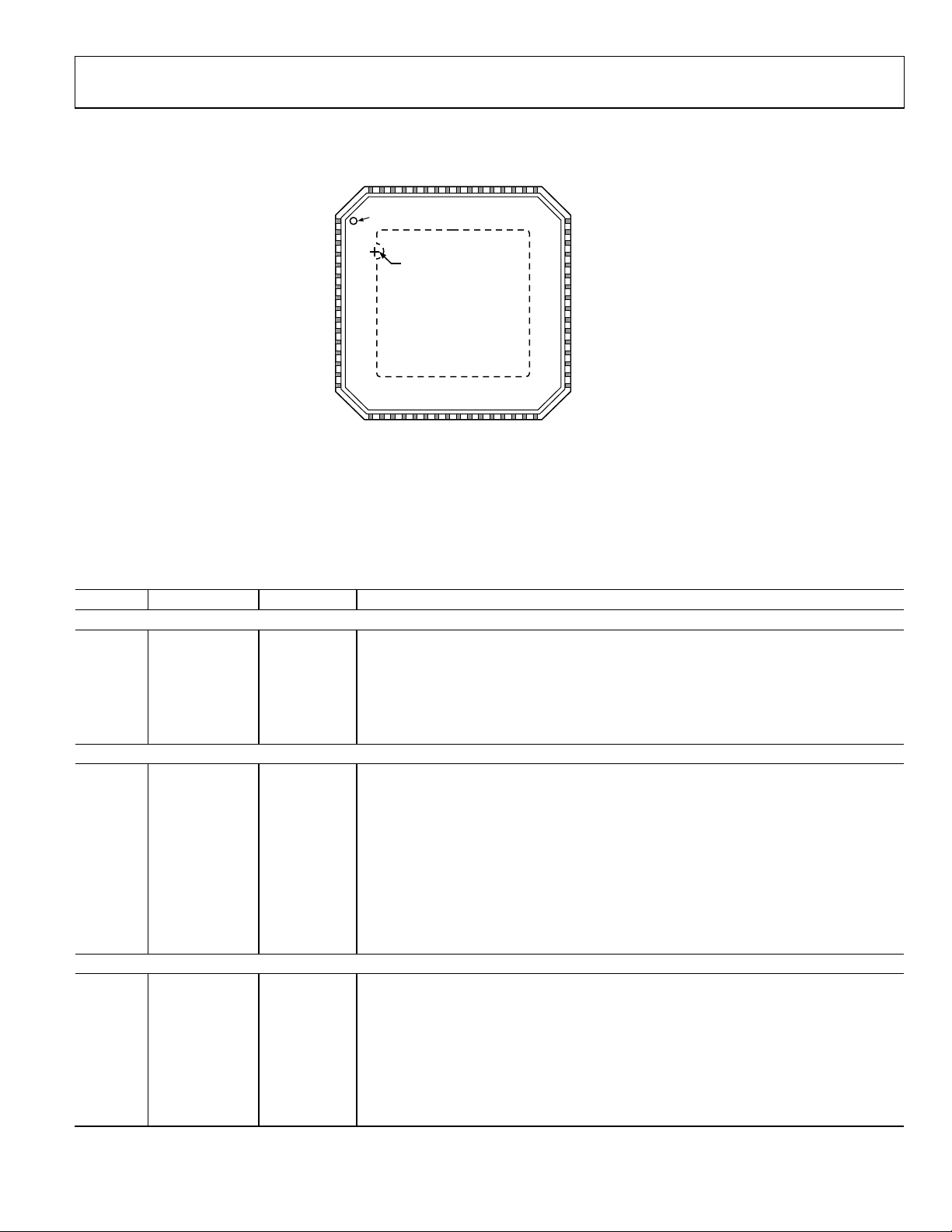
Figure 9. LFCSP Parallel CMOS Pin Configuration (Top View)
Table 12. Pin Function Descriptions (Parallel CMOS Mode)
Pin No. Mnemonic Type Description
ADC Power Supplies
20, 64 DRGND Ground Digital Output Ground.
1, 21 DRVDD Supply Digital Output Driver Supply (1.8 V to 3.3 V).
24, 57 DVDD Supply Digital Power Supply (1.8 V Nominal).
36, 45, 46 AVDD Supply Analog Power Supply (1.8 V Nominal).
0
AGND,
Exposed Pad
Ground
Analog Ground. The exposed thermal pad on the bottom of the package provides the
analog ground for the part. This pad must be connected to ground for proper operation.
ADC Analog
37 VIN+A Input Differential Analog Input Pin (+) for Channel A.
38 VIN−A Input Differential Analog Input Pin (−) for Channel A.
44 VIN+B Input Differential Analog Input Pin (+) for Channel B.
43 VIN−B Input Differential Analog Input Pin (−) for Channel B.
39 VREF Input/Output Voltage Reference Input/Output.
40 SENSE Input Voltage Reference Mode Select. (See Table 15 for details.)
42 RBIAS Input/Output External Reference Bias Resistor.
41 CML Output Common-Mode Level Bias Output for Analog Inputs.
49 CLK+ Input ADC Clock Input—True.
50 CLK− Input ADC Clock Input—Complement.
ADC Fast Detect Outputs
29 FD0A Output Channel A Fast Detect Indicator. (See Table 21 for details.)
30 FD1A Output Channel A Fast Detect Indicator. (See Table 21 for details.)
31 FD2A Output Channel A Fast Detect Indicator. (See Table 21 for details.)
32 FD3A Output Channel A Fast Detect Indicator. (See Table 21 for details.)
53 FD0B Output Channel B Fast Detect Indicator. (See Table 21 for details.)
54 FD1B Output Channel B Fast Detect Indicator. (See Table 21 for details.)
55 FD2B Output Channel B Fast Detect Indicator. (See Table 21 for details.)
56 FD3B Output Channel B Fast Detect Indicator. (See Table 21 for details.)
Rev. A | Page 19 of 88

AD6655
Pin No. Mnemonic Type Description
Digital Input
52 SYNC Input Digital Synchronization Pin. Slave mode only.
Digital Outputs
12 D0A (LSB) Output Channel A CMOS Output Data.
13 D1A Output Channel A CMOS Output Data.
14 D2A Output Channel A CMOS Output Data.
15 D3A Output Channel A CMOS Output Data.
16 D4A Output Channel A CMOS Output Data.
17 D5A Output Channel A CMOS Output Data.
18 D6A Output Channel A CMOS Output Data.
19 D7A Output Channel A CMOS Output Data.
22 D8A Output Channel A CMOS Output Data.
23 D9A Output Channel A CMOS Output Data.
25 D10A Output Channel A CMOS Output Data.
26 D11A Output Channel A CMOS Output Data.
27 D12A Output Channel A CMOS Output Data.
28 D13A (MSB) Output Channel A CMOS Output Data.
58 D0B (LSB) Output Channel B CMOS Output Data.
59 D1B Output Channel B CMOS Output Data.
60 D2B Output Channel B CMOS Output Data.
61 D3B Output Channel B CMOS Output Data.
62 D4B Output Channel B CMOS Output Data.
63 D5B Output Channel B CMOS Output Data.
2 D6B Output Channel B CMOS Output Data.
3 D7B Output Channel B CMOS Output Data.
4 D8B Output Channel B CMOS Output Data.
5 D9B Output Channel B CMOS Output Data.
6 D10B Output Channel B CMOS Output Data.
7 D11B Output Channel B CMOS Output Data.
8 D12B Output Channel B CMOS Output Data.
9 D13B (MSB) Output Channel B CMOS Output Data.
11 DCOA Output Channel A Data Clock Output.
10 DCOB Output Channel B Data Clock Output.
SPI Control
48 SCLK/DFS Input SPI Serial Clock/Data Format Select Pin in External Pin Mode.
47 SDIO/DCS Input/Output SPI Serial Data I/O/Duty Cycle Stabilizer Pin in External Pin Mode.
51 CSB Input SPI Chip Select. Active low.
Signal Monitor Port
33 SMI SDO/OEB Input/Output Signal Monitor Serial Data Output/Output Enable Input (Active Low) in External Pin Mode.
35 SMI SDFS Output Signal Monitor Serial Data Frame Sync.
34 SMI SCLK/PDWN Input/Output Signal Monitor Serial Clock Output/Power-Down Input (Active High) in External Pin Mode.
Rev. A | Page 20 of 88
AD6655
DRGND
D0+ (LSB)
D0– (LSB)
FD3+
FD3–
FD2+
FD2–
DVDD
FD1+
FD1–
FD0+
FD0–
SYNC
CSB
CLK–
646362616059585756555453525150
CLK+
49
DRVDD
D1–
D1+
D2–
D2+
D3–
D3+
D4–
D4+
DCO–
10
DCO+
11
D5–
12
D5+
13
D6–
14
D6+
15
D7–
16
NOTES
1. THE EXPOSED THERMAL PAD ON THE BOTTO M OF THE PACKAGE PROVIDES T HE
ANALOG GROUND FOR THE PART. THIS EXPOSE D PAD MUST BE CONNECT ED TO
GROUND FOR PROPER OPERATION.
PIN 1
1
INDICATOR
2
3
4
5
6
7
8
9
EXPOSED PADDLE, PIN 0
(BOTTOM OF PACKAGE)
AD6655
PARALLEL LVDS
TOP VIEW
(Not to S cale)
171819202122232425262728293031
D8–
D7+
D9–
D8+
D9+
D10–
D11–
D12–
D10+
D11+
DRGND
DVDD
DRVDD
D12+
48
SCLK/DFS
47
SDIO/DCS
46
AVDD
45
AVDD
44
VIN+B
43
VIN–B
42
RBIAS
41
CML
40
SENSE
39
VREF
38
VIN–A
37
VIN+A
36
AVDD
35
SMI SDFS
34
SMI SCLK/PDWN
33
SMI SDO/OEB
32
D13– (MSB)
D13+ (MSB)
06709-003
Figure 10. LFCSP Interleaved Parallel LVDS Pin Configuration (Top View)
Table 13. Pin Function Descriptions (Interleaved Parallel LVDS Mode)
Pin No. Mnemonic Type Description
ADC Power Supplies
20, 64 DRGND Ground Digital Output Ground.
1, 21 DRVDD Supply Digital Output Driver Supply (1.8 V to 3.3 V).
24, 57 DVDD Supply Digital Power Supply (1.8 V Nominal.)
36, 45, 46 AVDD Supply Analog Power Supply (1.8 V Nominal.)
0
AGND,
Exposed Pad
Ground
Analog Ground. The exposed thermal pad on the bottom of the package provides the analog
ground for the part. This exposed pad must be connected to ground for proper operation.
ADC Analog
37 VIN+A Input Differential Analog Input Pin (+) for Channel A.
38 VIN−A Input Differential Analog Input Pin (−) for Channel A.
44 VIN+B Input Differential Analog Input Pin (+) for Channel B.
43 VIN−B Input Differential Analog Input Pin (−) for Channel B.
39 VREF Input/Output Voltage Reference Input/Output.
40 SENSE Input Voltage Reference Mode Select. See Table 15 for details.
42 RBIAS Input/Output External Reference Bias Resistor.
41 CML Output Common-Mode Level Bias Output for Analog Inputs.
49 CLK+ Input ADC Clock Input—True.
50 CLK− Input ADC Clock Input—Complement.
ADC Fast Detect Outputs
54 FD0+ Output Channel A/Channel B LVDS Fast Detect Indicator 0—True. See Table 21 for details.
53 FD0- Output Channel A/Channel B LVDS Fast Detect Indicator 0—Complement. See Table 21 for details.
56 FD1+ Output Channel A/Channel B LVDS Fast Detect Indicator 1—True. See Table 21 for details.
55 FD1− Output Channel A/Channel B LVDS Fast Detect Indicator 1—Complement. See Table 21 for details.
59 FD2+ Output Channel A/Channel B LVDS Fast Detect Indicator 2—True See Table 21 for details.
58 FD2− Output Channel A/Channel B LVDS Fast Detect Indicator 2—Complement. See Table 21 for details.
61 FD3+ Output Channel A/Channel B LVDS Fast Detect Indicator 3—True. See Table 21 for details.
60 FD3− Output Channel A/Channel B LVDS Fast Detect Indicator 3—Complement. See Table 21 for details.
Rev. A | Page 21 of 88

AD6655
Pin No. Mnemonic Type Description
Digital Input
52 SYNC Input Digital Synchronization Pin. Slave mode only.
Digital Outputs
63 D0+ (LSB) Output Channel A/Channel B LVDS Output Data 0—True.
62 D0− (LSB) Output Channel A/Channel B LVDS Output Data 0—Complement.
3 D1+ Output Channel A/Channel B LVDS Output Data 1—True.
2 D1− Output Channel A/Channel B LVDS Output Data 1—Complement.
5 D2+ Output Channel A/Channel B LVDS Output Data 2—True.
4 D2− Output Channel A/Channel B LVDS Output Data 2—Complement.
7 D3+ Output Channel A/Channel B LVDS Output Data 3—True.
6 D3− Output Channel A/Channel B LVDS Output Data 3—Complement.
9 D4+ Output Channel A/Channel B LVDS Output Data 4—True.
8 D4− Output Channel A/Channel B LVDS Output Data 4—Complement.
13 D5+ Output Channel A/Channel B LVDS Output Data 5—True.
12 D5− Output Channel A/Channel B LVDS Output Data 5—Complement.
15 D6+ Output Channel A/Channel B LVDS Output Data 6—True.
14 D6− Output Channel A/Channel B LVDS Output Data 6—Complement.
17 D7+ Output Channel A/Channel B LVDS Output Data 7—True.
16 D7− Output Channel A/Channel B LVDS Output Data 7—Complement.
19 D8+ Output Channel A/Channel B LVDS Output Data 8—True.
18 D8− Output Channel A/Channel B LVDS Output Data 8—Complement.
23 D9+ Output Channel A/Channel B LVDS Output Data 9—True.
22 D9− Output Channel A/Channel B LVDS Output Data 9—Complement.
26 D10+ Output Channel A/Channel B LVDS Output Data 10—True.
25 D10− Output Channel A/Channel B LVDS Output Data 10—Complement.
28 D11+ Output Channel A/Channel B LVDS Output Data 11—True.
27 D11− Output Channel A/Channel B LVDS Output Data 11—Complement.
30 D12+ Output Channel A/Channel B LVDS Output Data 12—True.
29 D12− Output Channel A/Channel B LVDS Output Data 12—Complement.
32 D13+ (MSB) Output Channel A/Channel B LVDS Output Data 13—True.
31 D13− (MSB) Output Channel A/Channel B LVDS Output Data 13—Complement.
11 DCO+ Output Channel A/Channel B LVDS Data Clock Output—True.
10 DCO− Output Channel A/Channel B LVDS Data Clock Output—Complement.
SPI Control
48 SCLK/DFS Input SPI Serial Clock/Data Format Select Pin in External Pin Mode.
47 SDIO/DCS Input/Output SPI Serial Data I/O/Duty Cycle Stabilizer in External Pin Mode.
51 CSB Input SPI Chip Select (Active Low).
Signal Monitor Port
33 SMI SDO/OEB Input/Output Signal Monitor Serial Data Output/Output Enable Input (Active Low) in External Pin Mode.
35 SMI SDFS Output Signal Monitor Serial Data Frame Sync.
34 SMI SCLK/PDWN Input/Output Signal Monitor Serial Clock Output/Power-Down Input (Active High) in External Pin Mode.
Rev. A | Page 22 of 88

AD6655
V
EQUIVALENT CIRCUITS
VIN
06709-004
Figure 11. Equivalent Analog Input Circuit
AVDD
SCLK/DFS
Figure 15. Equivalent SCLK/DFS Input Circuit
26kΩ
1kΩ
06709-008
CLK+
1.2V
10kΩ 10kΩ
Figure 12. Equivalent Clock lnput Circuit
DRVDD
DRGND
06709-006
Figure 13. Equivalent Digital Output Circuit
DRVDD
DRVDD
26kΩ
SDIO/DCS
1kΩ
CLK–
SENSE
06709-005
1kΩ
06709-009
Figure 16. Equivalent SENSE Circuit
AVDD
26kΩ
CSB
1kΩ
06709-010
Figure 17. Equivalent CSB Input Circuit
AVDD
REF
6kΩ
06709-007
Figure 14. Equivalent SDIO/DCS Circuit or SMI SDFS Circuit
Figure 18. Equivalent VREF Circuit
06709-011
.
Rev. A | Page 23 of 88
AD6655
TYPICAL PERFORMANCE CHARACTERISTICS
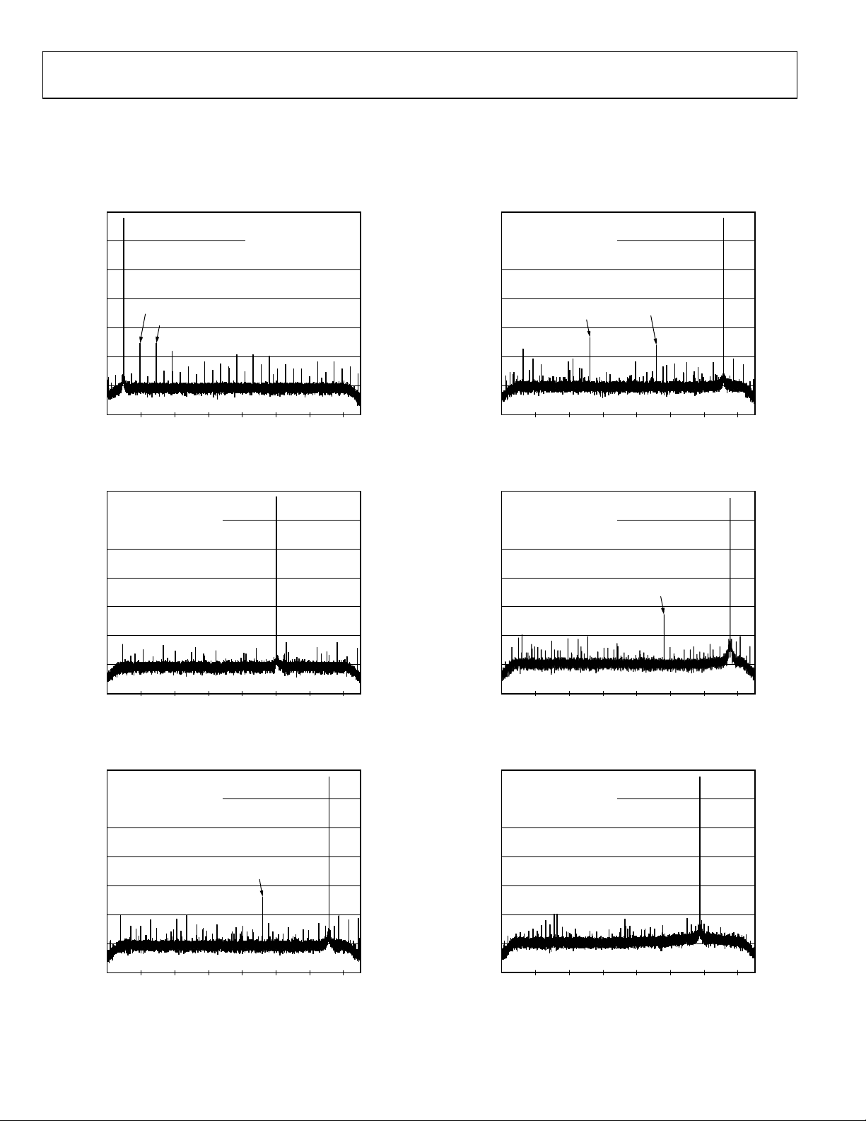
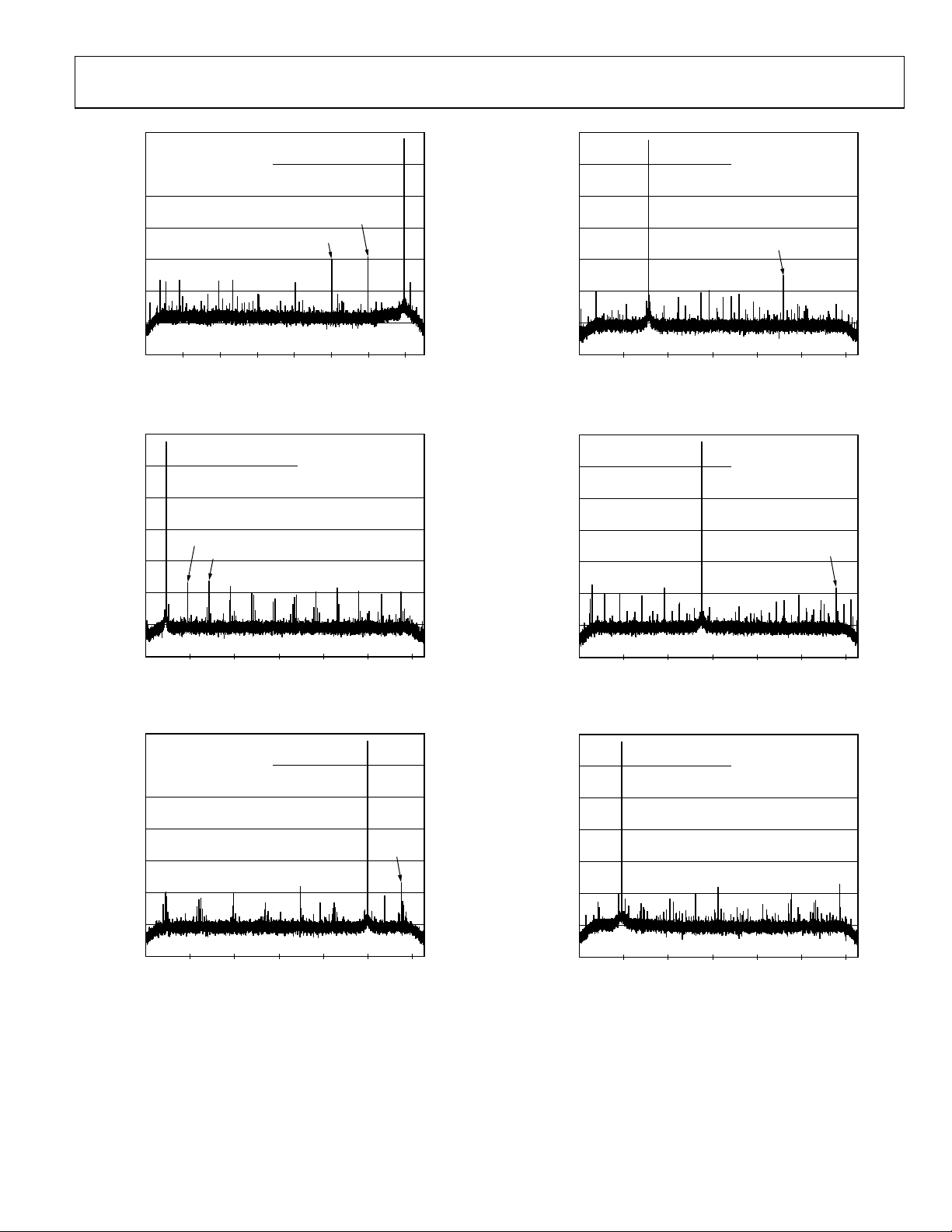
AVDD = 1.8 V, DVDD = 1.8 V, DRVDD = 1.8 V, sample rate = 150 MSPS, DCS enabled, 1.0 V internal reference, 2 V p-p differential
input, VIN = −1.0 dBFS, 64k sample, T
the location of the second and third harmonics is noted when they fall in the pass band of the filter.
0
–20
–40
= 25°C, NCO enabled, FIR filter enabled, unless otherwise noted. In the FFT plots that follow,
A
150MSPS
2.4MHz @ –1dBFS
SNR = 74.7dBc (75.7dBFS)
SFDR = 86.5dBc
f
= 18.75MHz
NCO
0
150MSPS
140.1MHz @ –1dBF S
SNR = 73.7dBc ( 7 4.7dBFS)
–20
SFDR = 82.8dBc
f
= 126MHz
NCO
–40
–60
–80
AMPLITUDE (dBFS)
–100
–120
–140
SECOND HARMONIC
THIRD HARMONIC
0330252015105
FREQUENCY (MHz)
Figure 19. AD6655-150 Single-Tone FFT with fIN = 2.4 MHz, f
0
150MSPS
30.3MHz @ –1dBFS
SNR = 74.8dBc ( 7 5.8dBFS)
–20
SFDR = 100dBc
f
= 24MHz
NCO
–40
–60
–80
AMPLITUDE (dBFS)
–100
–120
–140
0330252015105
FREQUENCY (MHz)
Figure 20. AD6655-150 Single-Tone FFT with fIN = 30.3 MHz, f
0
150MSPS
140.1MHz @ –1dBF S
SNR = 74.3dBc ( 7 5.3dBFS)
–20
SFDR = 83.3dBc
f
= 56MHz
NCO
–40
–60
–80
AMPLITUDE (dBFS)
–100
–120
–140
5
06709-018
= 18.75 MHz
NCO
5
06709-019
= 24 MHz
NCO
0330252015105
Figure 22. AD6655-150 Single-Tone FFT with fIN = 140.1 MHz,
0
150MSPS
220.1MHz @ –1dBF S
SNR = 71.8dBc ( 7 2.8dBFS)
–20
SFDR = 81.4dBc
f
NCO
–40
–60
–80
AMPLITUDE (dBFS)
–100
–120
–140
0330252015105
Figure 23. AD6655-150 Single-Tone FFT with fIN = 220.1 MHz,
0
150MSPS
332.1MHz @ –1dBF S
SNR = 71.7dBc ( 7 2.7dBFS)
–20
SFDR = 95.0dBc
f
NCO
–40
= 205MHz
= 321.5MHz
SECOND HARMONICTHIRD HARMONIC
FREQUENCY (MHz)
= 126 MHz
f
NCO
THIRD HARMONIC
FREQUENCY (MHz)
= 205 MHz
f
NCO
5
06709-021
5
06709-022
–60
–80
AMPLITUDE (dBFS)
–100
–120
–140
0330252015105
THIRD HARMONIC
FREQUENCY (MHz)
Figure 21. AD6655-150 Single-Tone FFT with fIN = 70.1 MHz, f
–60
–80
AMPLITUDE (dBFS)
–100
–120
–140
5
06709-020
= 56 MHz
NCO
0330252015105
Figure 24. AD6655-150 Single-Tone FFT with fIN = 332.1 MHz,
Rev. A | Page 24 of 88
FREQUENCY (MHz)
= 321.5 MHz
f
NCO
5
06709-023
AD6655
0
150MSPS
445.1MHz @ –1dBF S
SNR = 67.4dBc ( 6 5.4dBFS)
–20
SFDR = 74.1dBc
f
= 429MHz
NCO
–40
–60
–80
AMPLITUDE (dBFS)
–100
SECOND HARMONIC
THIRD HARMONIC
0
–20
–40
–60
–80
AMPLITUDE (dBFS)
–100
125MSPS
70.3MHz @ –1dBFS
SNR = 74.6dBc (75.6dBFS)
SFDR = 86.1dBc
f
= 78MHz
NCO
THIRD HARMONIC
–120
–140
0330252015105
FREQUENCY (MHz)
Figure 25. AD6655-150 Single-Tone FFT with fIN = 445.1 MHz, f
AMPLITUDE (dBFS)
0
–20
–40
–60
–80
–100
–120
–140
SECOND HARMONIC
THIRD HARMONIC
03252015105
FREQUENCY (MHz)
125MSPS
2.4MHz @ –1dBFS
SNR = 74.5dBc (75.5dBFS)
SFDR = 87.8dBc
f
= 15.75MHz
NCO
Figure 26. AD6655-125 Single-Tone FFT with fIN =2.4 MHz, f
0
125MSPS
30.3MHz @ –1dBFS
SNR = 74.7dBc ( 7 5.7dBFS)
–20
SFDR = 89.6dBc
f
= 21MHz
NCO
–40
–120
–140
AMPLITUDE (dBFS)
–20
–40
–60
–80
–100
–120
–140
–20
–40
03252015105
0
03252015105
0
5
06709-024
= 429 MHz
NCO
0
06709-025
= 15.75 MHz
NCO
Figure 28. AD6655-125 Single-Tone FFT with fIN = 70.3 MHz, f
Figure 29. AD6655-125 Single-Tone FFT with fIN = 140.1 MHz, f
FREQUENCY (MHz)
125MSPS
140.1MHz @ –1dBF S
SNR = 74.1dBc (75.1dBFS)
SFDR = 90.3dBc
f
NCO
FREQUENCY (MHz)
125MSPS
220.1MHz @ –1dBF S
SNR = 73.4dBc (74.4dBFS)
SFDR = 90.2dBc
f
NCO
NCO
= 142MHz
THIRD HARMONIC
NCO
= 231MHz
0
06709-027
= 78 MHz
0
06709-028
= 142 MHz
–60
HARMONIC
AMPLITUDE (dBFS)
–80
–100
–120
–140
03252015105
FREQUENCY (MHz)
Figure 27. AD6655-125 Single-Tone FFT with fIN = 30.3 MHz, f
THIRD
0
06709-026
= 21 MHz
NCO
–60
–80
AMPLITUDE (dBFS)
–100
–120
–140
03252015105
Figure 30. AD6655-125 Single-Tone FFT with fIN = 220.1 MHz, f
Rev. A | Page 25 of 88
FREQUENCY (MHz)
0
06709-029
= 231 MHz
NCO
AD6655
120
95
SNR/SFDR (d Bc AND d BFS)
100
80
60
40
20
0
–90 0–10–20–30–40–50–60–70–80
SNR (dBFS)
SFDR (dBc)
SFDR (dBFS)
85dB
REFERENCE LINE
SNR (dBc)
INPUT AMPLITUDE (dBFS)
06709-030
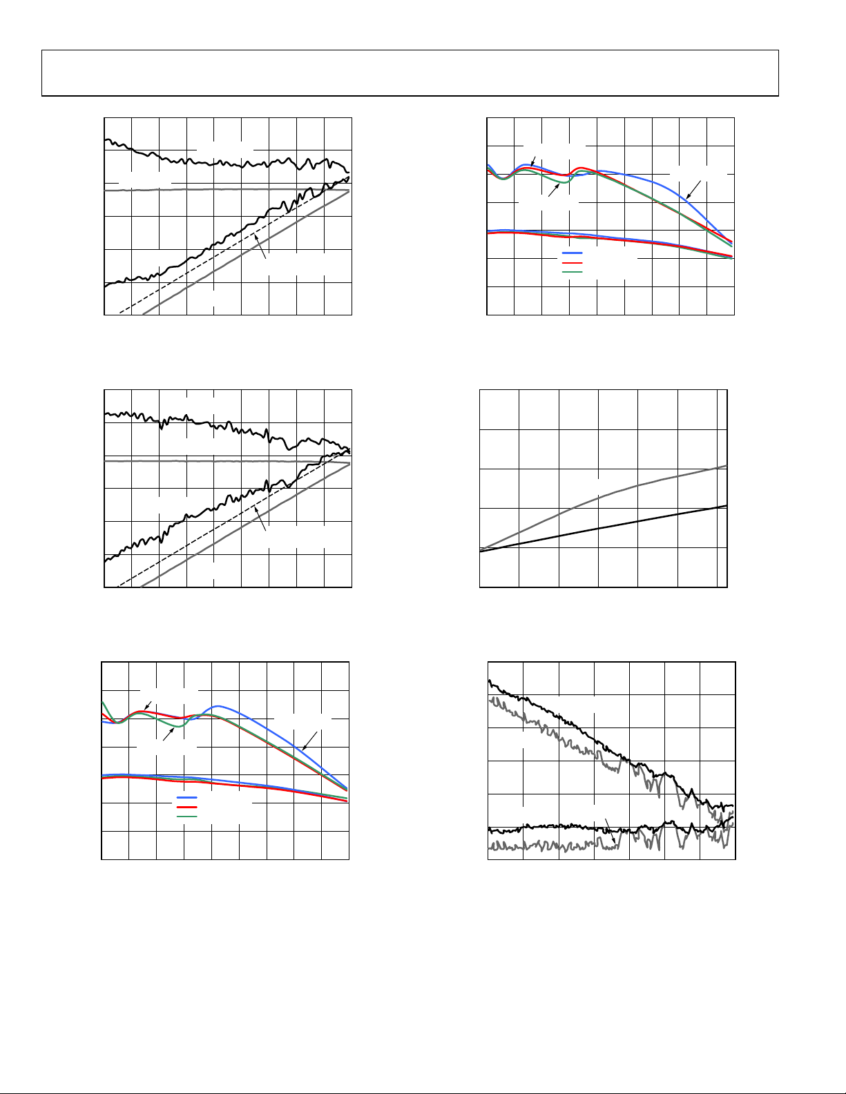
Figure 31. AD6655-150 Single-Tone SNR/SFDR vs. Input Amplitude (AIN) with
SNR/SFDR (d Bc AND d BFS)
120
100
80
60
40
20
0
–90 0–10–20–30–40–50–60–70–80
= 2.4 MHz, f
f
IN
SFDR (dBFS)
SNR (dBFS)
SFDR (dBc)
INPUT AMPLITUDE (dBFS)
NCO
SNR (dBc)
= 18.75 MHz
85dB
REFERENCE LINE
06709-031
Figure 32. AD6655-150 Single-Tone SNR/SFDR vs. Input Amplitude (AIN) with
= 98.12 MHz, f
f
IN
95
= 100.49 MHz
NCO
90
85
80
75
SNR/SFDR (dBc)
70
65
60
0440035030025020015010050
SFDR = +85°C
SFDR = –40°C
INPUT FREQ UENCY ( MHz )
SNR = +25°C
SNR = +85°C
SNR = –40°C
SFDR = +25°C
50
06709-033
Figure 34. AD6655-125 Single-Tone SNR/SFDR vs. Input Frequency (fIN) and
Temperature with DRVDD = 3.3 V
–1.5
–2.0
–2.5
–3.0
GAIN E RROR (%F SR)
–3.5
–4.0
–40 806040200–20
OFFSET
GAIN
TEMPERATURE (°C)
0.5
0.4
0.3
0.2
OFFSET ERROR (%FSR)
0.1
0
Figure 35. AD6655-150 Gain and Offset vs. Temperature
0
06709-034
90
85
80
75
SNR/SFDR (dBc)
70
65
60
045040035030025020015010050
SFDR = +85°C
SFDR = –40°C
INPUT FREQ UENCY ( MHz )
SNR = +25°C
SNR = +85°C
SNR = –40°C
SFDR = +25°C
06709-032
Figure 33. AD6655-125 Single-Tone SNR/SFDR vs. Input Frequency (fIN) and
Temperature with DRVDD = 1.8 V
Rev. A | Page 26 of 88
–20
–40
IMD3 (dBc)
–60
–80
SFDR (dBFS)
SFDR/IM D3 ( dBc AND dBFS)
–100
–120
–90 –78 –66 –54 –42 –30 –18 –6
SFDR (dBc)
IMD3 (dBFS )
INPUT AMPLITUDE (dBF S )
Figure 36. AD6655-150 Two-Tone SFDR/IMD3 vs. Input Amplitude (AIN) with
f
= 29.12 MHz, f
IN1
= 32.12 MHz, fS = 150 MSPS, f
IN2
= 22 MHz
NCO
06709-035
AD6655
0
–20
–40
IMD3 (dBc)
–60
–80
SFDR (dBFS)
SFDR/IM D3 ( dBc AND dBFS)
–100
SFDR (dBc)
IMD3 (dBFS )
0
–20
–40
–60
–80
AMPLITUDE (dBFS)
–100
–120
150MSPS
169.12MHz @ –7dBFS
172.12MHz @ –7dBFS
SFDR = 85.5d Bc (92.5dBFS )
f
= 177MHz
NCO
–120
–90 –78 –66 –54 –42 –30 –18 –6
INPUT AMPLITUDE (dBF S )
06709-036
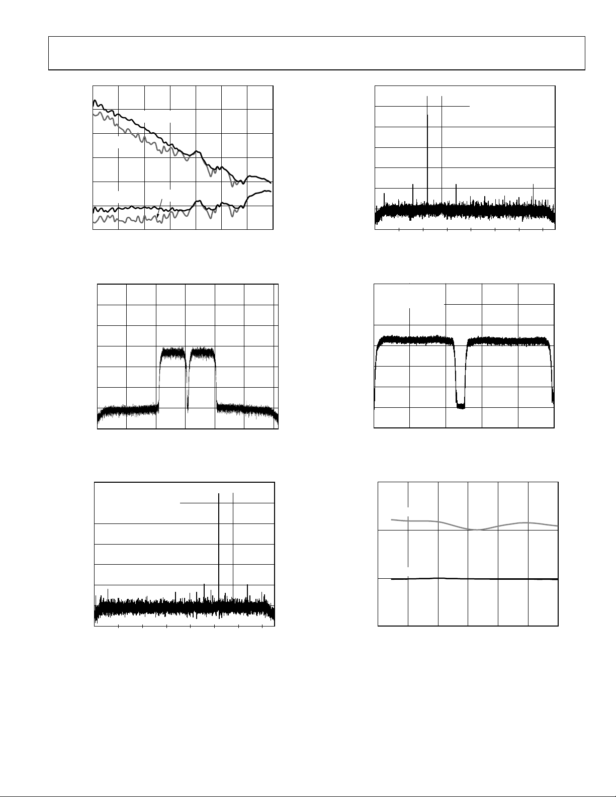
Figure 37. AD6655-150 Two-Tone SFDR/IMD3 vs. Input Amplitude (AIN) with
= 169.12 MHz, f
f
IN1
0
–20
–40
–60
–80
AMPLITUDE (dBFS)
–100
–120
–140
0 5 10 15 20 25 30
= 172.12 MHz, fS = 150 MSPS, f
IN2
FREQUENCY (MHz)
= 177 MHz
NCO
06709-037
Figure 38. AD6655-125, Two 64k WCDMA Carriers with fIN = 170 MHz,
= 122.88 MHz, f
f
S
0
150MSPS
29.12MHz @ –7dBF S
32.12MHz @ –7dBF S
–20
SFDR = 89.1d Bc ( 96.1dBFS)
f
= 22MHz
NCO
–40
–60
= 168.96 MHz
NCO
–140
0330252015105
FREQUENCY (MHz)
Figure 40. AD6655-150 Two Tone FFT with f
= 172.12 MHz, fS = 150 MSPS, f
f
IN2
0
NPR = 64.5dBc
NOTCH @ 18.5MHz
NOTCH WIDTH = 3MHz
–20
–40
–60
–80
AMPLITUDE (dBFS)
–100
–120
–140
0330.022.515.07.5
FREQUENCY (MHz )
Figure 41. AD6655-150 Noise Power Ratio (NPR)
95
SFDR (dBc)
85
= 169.12 MHz,
IN1
= 177 MHz
NCO
5
06709-039
7.5
06709-040
–80
AMPLITUDE (dBFS)
–100
–120
–140
0330252015105
FREQUENCY (MHz)
Figure 39. AD6655-150 Two-Tone FFT with f
= 150 MSPS, f
f
S
NCO
= 29.12 MHz, f
IN1
= 22 MHz
SNR/SFDR (dBc)
75
65
5
06709-038
= 32.12 MHz,
IN2
Figure 42. AD6655-150 Single-Tone SNR/SFDR vs. Sample Rate (fs) with
0 25 50 75 100 125 150
Rev. A | Page 27 of 88
SNR (dBc)
SAMPLE RATE (MSPS)
= 2.3 MHz
f
IN
06709-041
 Loading...