14-Bit, 92.16 MSPS, 4-/6-Channel
A
www.BDTIC.com/ADI
FEATURES
SNR = 90 dB in 1.25 MHz bandwidth to Nyquist
SNR = 87 dB in 1.25 MHz bandwidth to 200 MHz
Integrated 14-bit, 92.16 MSPS ADC
IF sampling frequencies to 200 MHz
Internal 2.4 V reference, 2.2 V p-p analog input range
Internal differential track-and-hold analog input
Processes 4/6 wideband carriers simultaneously
Fractional clock multiplier to 200 MHz
Programmable decimating FIR filters, interpolating
half-band filters and programmable AGC loops
with 96 dB range
Three 16-bit configurable parallel output ports
User-configurable built-in self-test (BIST) capability
8-/16-bit microport and SPORT/SPI® serial port control
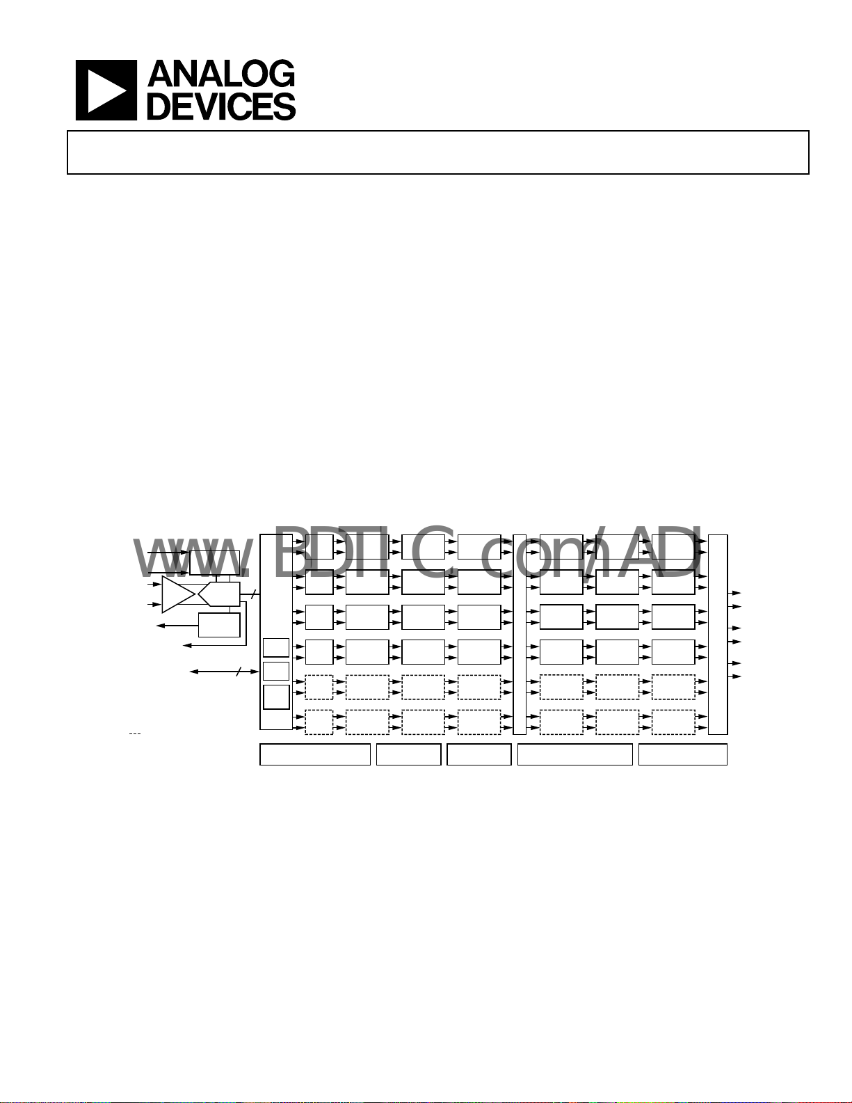
FUNCTIONAL BLOCK DIAGRAM
Wideband IF to Baseband Receiver
AD6654
APPLICATIONS
Multicarrier, multimode digital receivers
GSM, EDGE, PHS, UMTS, WCDMA, CDMA2000,
TD-SCDMA, WiMAX
Micro and pico cell systems, software radios
Wireless local loop
Smart antenna systems
In-building wireless telephony
Broadband data applications
Instrumentation and test equipment
14-BIT ADC FRONT END
ENC+
ENC–
AIN+
AIN–
V
REF
(ADC OVERRANGE)
(VGA LEVEL CONTROL)
(AVAILABLE IN
6-CHANNEL MODEL ONLY)
M = DECIMATION
L = INTERPOLATION
SHA
OVR
EXP
INTERNAL
TIMING
ADC
2.4V
V
REF
14
INPUT
MATRIX
PRN
GEN
3
EXP
BITS
PEAK/
RMS
MSMT
VDDCORE, VDDIO, GND
NCO
NCO
NCO
NCO
NCO
NCO
AVDD, DRVDD,
4-CHANNEL AND 6-CHANNEL DIGITAL DOWN CONVERTER
CIC5
M = 1–32
CIC5
M = 1–32
CIC5
M = 1–32
CIC5
M = 1–32
CIC5
M = 1–32
CIC5
M = 1–32
M = BYP, 2
M = BYP, 2
M = BYP, 2
M = BYP, 2
M = BYP, 2
M = BYP, 2
SYNC
0, 1, 2, 3
FIR1
HB1
FIR1
HB1
FIR1
HB1
FIR1
HB1
FIR1
HB1
FIR1
HB1
FIR2
HB2
M = BYP, 2
FIR2
HB2
M = BYP, 2
FIR2
HB2
M = BYP, 2
FIR2
HB2
M = BYP, 2
FIR2
HB2
M = BYP, 2
FIR2
HB2
M = BYP, 2
CLOCK
MULTIPLIER
MRCF
DRCF
M = 1–16
MRCF
DRCF
M = 1–16
MRCF
DRCF
M = 1–16
MRCF
DRCF
M = 1–16
DATA ROUTER MATRIX
MRCF
DRCF
M = 1–16
MRCF
DRCF
M = 1–16
8-BIT/16-BIT MICROPORT
INTERFACE
CRCF
M = 1–16
CRCF
M = 1–16
CRCF
M = 1–16
CRCF
M = 1–16
CRCF
M = 1–16
CRCF
M = 1–16
LHB
L = 1, 2
LHB
L = 1, 2
LHB
L = 1, 2
LHB
L = 1, 2
LHB
L = 1, 2
LHB
L = 1, 2
SPORT/
SPI INTERFACE
P
DATA ROUTING
AGC
PB
PC
PARALLEL PORTS
05156-001
Figure 1.
Rev. 0
Information furnished by Analog Devices is believed to be accurate and reliable.
However, no responsibility is assumed by Analog Devices for its use, nor for any
infringements of patents or other rights of third parties that may result from its use.
Specifications subject to change without notice. No license is granted by implication
or otherwise under any patent or patent rights of Analog Devices. Trademarks and
registered trademarks are the property of their respective owners.
One Technology Way, P.O. Box 9106, Norwood, MA 02062-9106, U.S.A.
Tel: 781.329.4700 www.analog.com
Fax: 781.461.3113 ©2005 Analog Devices, Inc. All rights reserved.

AD6654
www.BDTIC.com/ADI
TABLE OF CONTENTS
General Description......................................................................... 4
Input Crossbar Matrix ............................................................... 33
Product Highlights....................................................................... 5
Specifications..................................................................................... 6
Recommended Operating Conditions ...................................... 6
ADC DC Specifications............................................................... 6
ADC Digital Specifications ......................................................... 6
ADC Switching Specifications.................................................... 7
ADC AC Specifications ............................................................... 7
Electrical Characteristics............................................................. 8
Timing Characteristics ................................................................ 9
Microport Timing Characteristics ........................................... 10
Serial Port Timing Characteristics........................................... 11
Timing Diagrams............................................................................ 12
Absolute Maximum Ratings.......................................................... 18
Thermal Characteristics ............................................................ 18
Explanation of Test Levels......................................................... 18
Numerically Controlled Oscillator (NCO)................................. 34
NCO Frequency.......................................................................... 34
Mixer............................................................................................ 35
Bypass .......................................................................................... 35
Clear Phase Accumulator on Hop ........................................... 35
Phase Dither................................................................................ 35
Amplitude Dither....................................................................... 35
NCO Frequency Hold-Off Register ......................................... 35
Phase Offset................................................................................. 35
HOP Sync .................................................................................... 35
Fifth-Order CIC Filter ................................................................... 36
Bypass .......................................................................................... 36
CIC Rejection.............................................................................. 36
Example Calculations................................................................ 37
FIR Half-Band Block...................................................................... 38
ESD Caution................................................................................ 18
Pin Configuration and Function Descriptions........................... 19
Typical Performance Characteristics ........................................... 22
ADC Equivalent Circuits............................................................... 25
Te r mi n ol o g y .................................................................................... 26
Theory of Operation ...................................................................... 27
ADC Architecture ...................................................................... 27
Application information................................................................ 28
ADC Configuration Notes ........................................................ 28
DDC Configuration Notes........................................................ 29
ADC Input Port Monitor Function.............................................. 31
Peak Detector Mode................................................................... 31
Mean Power Mode ..................................................................... 31
Threshold Crossing Mode......................................................... 32
Additional Control Bits ............................................................. 32
3-Tap Fixed coefficient Filter (FIR1)....................................... 38
Decimate-by-2 Half-Band Filter (HB1) .................................. 38
6-Tap Fixed Coefficient Filter (FIR2)...................................... 39
Decimate-by-2 Half-Band Filter (HB2) .................................. 39
Intermediate Data Router.............................................................. 41
Mono-Rate RAM Coefficient Filter (MRCF)............................. 42
Symmetry .................................................................................... 42
Clock Rate................................................................................... 42
Bypass .......................................................................................... 42
Scaling.......................................................................................... 42
Decimating RAM Coefficient Filter (DRCF) ............................. 43
Bypass .......................................................................................... 43
Scaling.......................................................................................... 43
Symmetry .................................................................................... 43
Coefficient Offset ....................................................................... 43
Rev. 0 | Page 2 of 88

AD6654
www.BDTIC.com/ADI
Decimation Phase .......................................................................43
HOP ..............................................................................................58
Maximum Number of Taps Calculated....................................43
Programming DRCF Registers for
an Asymmetrical Filter ...............................................................44
Programming DRCF Registers for a Symmetric Filter ..........44
Channel RAM Coefficient Filter (CRCF) ....................................45
Bypass ...........................................................................................45
Scaling...........................................................................................45
Symmetry .....................................................................................45
Coefficient Offset........................................................................45
Decimation Phase .......................................................................45
Maximum Number of TAPS Calculated ..................................45
Programming CRCF Registers for an
Asymmetrical Filter ....................................................................46
Programming CRCF Registers for a Symmetrical Filter .......46
Interpolating Half-Band Filter.......................................................47
Output Data Router ........................................................................48
Interleaving Data.........................................................................48
Automatic Gain Control.................................................................49
AGC Loop ....................................................................................49
Desired Signal Level Mode ........................................................50
Desired Clipping Level Mode....................................................52
AGC Synchronization.................................................................52
SYNC Process ..............................................................................52
Parallel Port Output ........................................................................53
Interleaved I/Q Mode.................................................................53
Parallel IQ Mode .........................................................................53
Master/Slave PCLK Modes ........................................................55
Parallel Port Pin Functions ........................................................56
Serial Port Control..........................................................................60
Hardware Interface .....................................................................60
SPI Mode Timing ........................................................................62
SPORT Mode Timing.................................................................64
Programming Indirect Addressed Registers
Using Serial Port..........................................................................67
Connecting the AD6654 Serial Port to a Blackfin DSP.........69
Microport .........................................................................................70
Intel (Inm) Mode ........................................................................70
Motorola (MNM) Mode ............................................................70
Accessing Multiple AD6654 Devices .......................................71
Memory Map ...................................................................................72
Reading the Memory Map Table...............................................72
Bit Format ....................................................................................72
Open Locations ...........................................................................72
Default Values..............................................................................72
Logic Levels..................................................................................72
Global Register Map...................................................................74
Input Port Register Map.............................................................76
Channel Register Map................................................................78
MRCF Coefficient Memory.......................................................79
Output Port Register Map..........................................................82
DDC Design Notes .........................................................................85
Outline Dimensions........................................................................87
Ordering Guide...........................................................................87
REVISION HISTORY
4/05—Revision 0: Initial Version
User-Configurable Built-In Self-Test (BIST)...............................57
Chip Synchronization.....................................................................58
Start ...............................................................................................58
Rev. 0 | Page 3 of 88

AD6654
www.BDTIC.com/ADI
GENERAL DESCRIPTION
The AD6654 is a mixed-signal IF-to-baseband receiver
consisting of a 14-bit, 92.16 MSPS analog-to-digital converter
(ADC) and a 4-/6-channel, multimode digital down-converter
(DDC) capable of processing up to six WCDMA (wideband
code division multiple access) channels. The AD6654 has been
optimized for the demanding filtering requirements of wideband standards such as CDMA2000, UMTS, and TD-SCDMA,
but is flexible enough to support wider standards such as
WiMAX. It is typically used as part of a radio system that
digitally demodulates and filters IF sampled signals.
The ADC stage features a high performance track-and-hold
in
put amplifier (T/H), integrated voltage reference, and 14-bit
sampling resolution. Input signals up to 200 MHz can be
accurately digitized at encode rates up to 92.16 MSPS. The ADC
data outputs are internally routed directly into the DDC inputs,
where down-conversion, decimation and digital filtering are
performed. An overrange (OVR) output bit provides indication
of excessive ADC input levels. An ADC data-ready (DR) output
bit provides a synchronized clock for the integrated DDC.
Data from the ADC is evaluated for peak or mean power in the
in
put stage of the DDC, and the result is available to the user via
control register access. The DDC input stage also outputs 3-bit
level-indicator data (EXP) bits that can be used to control the
gain of the external DVGA in 6 dB steps (up to 48 dB) to
optimize signal amplitude into the ADC input.
The DDC stage has the following signal processing stages: six
W
CDMA-ready channels, each consisting of a frequency
translator, a fifth-order cascaded integrated comb filter, two sets
of cascaded fixed coefficient FIR and half-band filters, three
cascaded programmable sum of product FIR filters, an
interpolating half-band filter (IHB), and a digital automatic
gain control (AGC) block. Multiple modes are supported for
clocking data out of the chip. Programming is accomplished via
serial or microport interfaces.
Frequency translation is accomplished with a 32-bit complex
n
umerically controlled oscillator (NCO). The NCO has greater
than 110 dBc SDFR. This stage translates a real input signal
from an intermediate frequency (IF) to a baseband complex
digital output. Phase and amplitude dither can be enabled onchip to improve spurious performance of the NCO. A 16-bit
phase-offset word is available to create a known phase relationship between multiple AD6654 chips or channels. The NCO can
also be bypassed.
Following frequency translation is a fifth-order CIC filter with a
p
rogrammable decimation between 1 and 32. This filter is used
to efficiently lower the sample rate, while providing sufficient
alias rejection at frequencies at higher offsets from the signal
of interest.
Following the CIC5 are two sets of filters. Each filter set
in
cludes a nondecimating FIR filter and a decimate-by-2 halfband filter. The FIR1 filter provides about 30 dB of rejection,
while the HB1 provides about 77 dB of rejection. These two sets
of filters can be used together to achieve a 107 dB stop-band
alias rejection, or they can be individually bypassed to save
power.
The FIR2 filter provides about 30 dB of rejection, while the HB2
f
ilter provides about 65 dB of rejection. The filters can be used
together to achieve more than 95 dB stop-band alias rejection,
or they can be individually bypassed to save power. FIR1 and
HB1 filters can run at the maximum ADC data port rate. In
contrast, FIR2 and HB2 can run with a maximum input rate of
75 MSPS (input rate to FIR2 and HB2 filters).
The programmable filtering is divided into three cascaded RAM
c
oefficient filters (RCFs) for flexible and power-efficient
filtering. The first filter in the cascade is the MRCF, consisting
of a programmable nondecimating FIR. It is followed by
programmable FIR filters (DRCF) with decimation from 1 to
16. They can be used either together to provide high rejection
filters, or independently to save power. The maximum input
rate to the MRCF is one-fourth the PLL clock rate.
The CRCF (Channel RCF) is the last programmable FIR filter
wi
th programmable decimation from 1 to 16. It is typically used
to meet the spectral mask requirements for the air standard of
interest. This could be an RRC, antialiasing filter or any other
real data filter. Decimation in preceding blocks is used to keep
the input rate of this stage as low as possible for the best filter
performance.
The last filter stage in the chain is an interpolate-by-2 half-band
f
ilter, which is used to up-sample the CRCF output to produce
higher output oversampling. Signal rejection requirements for
this stage are relaxed, because preceding filters have already
filtered the blockers and adjacent carriers.
The DDC input port of the AD6654 has its own clock input
used
for latching the input data, as well as for providing the
input for an onboard PLL clock multiplier. The output of the
PLL clock is used for processing all filters and processing blocks
beyond the data router following CIC filter. The PLL clock can
be programmed to have a maximum clock rate of 200 MHz.
Typically, the DDC input clock is driven directly from the
integrated ADC’s data-ready (DR) output to ensure proper
synchronization.
A data routing block is used to distribute data from the CICs to
th
e various channel filters. This block allows multiple back-end
filter chains to work together to process high bandwidth signals
or to make even sharper filter transitions than a single channel
Rev. 0 | Page 4 of 88

AD6654
www.BDTIC.com/ADI
can perform. It can also allow complex filtering operations to be
achieved in the programmable filters.
The digital AGC provides the user with scaled digital outputs
ased on the rms level of the signal present at the output of the
b
digital filters. The user can set the requested level and time
constant of the AGC loop for optimum performance of the
postprocessor. This is a critical function in the base station for
CDMA application, where the power level must be well
controlled going into the RAKE receivers. It has programmable
clipping and rounding control to provide different output
resolutions.
Channel 5 are not available (see Figure 1). The 4-channel device
has the same DDC input port features, output ports, and
memory map as the 6-channel device. On the 4-channel
version, the memory map section for Channel 4 and Channel 5
can be programmed and read back, but the two extra channels
are disabled internally.
PRODUCT HIGHLIGHTS
1. Integrated 14-bit, 92.16 MSPS ADC.
2. T
rack-and-hold amplifier analog input for excellent IF
sampling up to 200 MHz.
The overall filter response for the AD6654 is the composite of
al
l the combined filter stages. Each successive filter stage is
capable of narrower transition bandwidths, but requires a
greater number of CLK cycles to calculate the output. The
AD6654 features a fractional clock multiplier that uses the ADC
clock (which is slower than the DDC’s processing speed) to
produce a DDC master clock up to 200 MHz. This feature
allows fractional multiplication of the input clock to allow the
DDC to function at maximum speed while maintaining edge
identity to the ADC clock.
More decimation in the first filter stage minimizes overall
p
ower consumption. Data from the device is interfaced to a
DSP/FPGA/baseband processor via high speed parallel ports
(preferred), or a DSP-compatible microprocessor interface.
The AD6654 is available in 4-channel and 6-channel versions.
The p
rimary focus of the data sheet is on the 6-channel part.
The only difference between the 6-channel and 4-channel
devices is that, on the 4-channel version, Channel 4 and
3. F
our or six independent digital filtering channels.
4. R
MS/peak power monitoring of the ADC data port and
96 dB range AGCs before the output ports.
5. Thr
6. C
7. T
8. Black
9. S
ee programmable RAM coefficient filters, three halfband filters, two fixed coefficient filters, and one fifthorder CIC filter per channel.
omplex filtering by combining filtering capability of
multiple channels.
hree 16-bit parallel output ports operating at up to
200 MHz clock.
fin®- and TigerSHARC®-compatible, 8-/16-bit
microprocessor port.
ynchronous serial communications port is compatible
with most serial interface standards: SPORT, SPI, and SSR.
Rev. 0 | Page 5 of 88

AD6654
www.BDTIC.com/ADI
SPECIFICATIONS
RECOMMENDED OPERATING CONDITIONS
Table 1.
Parameter (Conditions) Temp Test Level Min Typ Max Unit
1
AVDD
2
DRVDD
VDDCORE Full IV 1.65 1.8 1.95 V
2
VDDIO
T
AMBIENT
1
Specified for dc supplies with linear rise-time <250 ms.
2
DRVDD and VDDIO can be operated from the same supply.
ADC DC SPECIFICATIONS
AVDD = 5.0 V, DRVDD = 3.3 V, VDDCORE = 1.8 V, VDDIO = 3.3 V, maximum rated sample rate, differential ENC and AIN, unless
otherwise noted.
Table 2.
Parameter (Conditions) Temp Test Level Min Typ Max Unit
RESOLUTION Full IV 14 Bits
INTERNAL VOLTAGE REFERENCE (V
Output Voltage Full IV 2.4 V
ANALOG INPUTS
Differential Input Voltage Range Full IV 2.2 V p-p
Differential Input Capacitance Full V 1.5 pF
Differential Input Resistance Full V 1 kΩ
Power Supply Rejection (PSRR) 25°C V ±1.0 mV/V
1
V
is provided for setting the common-mode offset of a differential amplifier such as the AD8138 when a dc-coupled analog input is required. V
REF
if used to drive additional circuit functions.
REF
1
)
Full IV 4.75 5.0 5.25 V
Full IV 3.0 3.3 3.6 V
Full IV 3.0 3.3 3.6 V
IV −25 +25 +85 °C
should be buffered
REF
ADC DIGITAL SPECIFICATIONS
AVDD = 5.0 V, DRVDD = 3.3 V, VDDCORE = 1.8 V, VDDIO = 3.3 V, maximum rated sample rate, differential ADC input, unless
otherwise noted.
Table 3.
Parameter (Conditions) Temp Test Level Min Typ Max Unit
ENCODE INPUTS (ENC+, ENC−)
Differential Input Voltage Full IV 0.4 V p-p
Differential Input Resistance 25°C V 10 kΩ
Differential Input Capacitance 25°C V 2.5 pF
Rev. 0 | Page 6 of 88

AD6654
www.BDTIC.com/ADI
ADC SWITCHING SPECIFICATIONS
AVDD = 5.0 V, DRVDD = 3.3 V, VDDCORE = 1.8 V, VDDIO = 3.3 V, maximum rated sample rate, differential input, unless
otherwise noted.
Table 4.
Parameter (Conditions) Temp Test Level Min Typ Max Unit
SWITCHING PERFORMANCE
Maximum Conversion Rate Full II 92.16 MSPS
Minimum Conversion Rate Full IV 30 MSPS
ENC Pulse Width High1 (t
ENC Pulse Width Low1 (t
1
Several internal timing parameters are a function of t
ADC AC SPECIFICATIONS
AVDD = 5.0 V, DRVDD = 3.3 V, VDDCORE = 1.8 V, VDDIO = 3.3 V, maximum rated sample rate, differential input, unless
otherwise noted.
Table 5.
Parameter (Conditions) Temp Test Level Min Typ Max Unit
SIGNAL-TO-NOISE RATIO1 (WITHOUT HARMONICS)
Analog Input Frequency 37 MHz
ADC (46.08 MHz BW) 25°C V 74.5 dB
CDMA (1.25 MHz BW) Full II 88 90.0 dB
WCDMA (5.0 MHz BW) 25°C V 84 dB
Analog Input Frequency 70 MHz
ADC (46.08 MHz BW) 25°C V 73.5 dB
CDMA (1.25 MHz BW) Full II 87.5 89 dB
WCDMA (5.0 MHz BW) 25°C V 83 dB
Analog Input Frequency 150 MHz
ADC (46.08 MHz BW) 25°C V 73 dB
CDMA (1.25 MHz BW) 25°C V 88 dB
WCDMA (5.0 MHz BW) 25°C V 82 dB
Analog Input Frequency 200 MHz
ADC (46.08 MHz BW) 25°C V 72 dB
CDMA (1.25 MHz BW) 25°C V 87 dB
WCDMA (5.0 MHz BW) 25°C V 81 dB
WORST HARMONIC2 (ANALOG INPUT @ −1 dBFS)
37 MHz Full II 85 93 dBc
70 MHz Full V 91 dBc
150 MHz Full V 71 dBc
200 MHz Full V 63 dBc
INTERMODULATION DISTORTION (TWO-TONES SEPARATED BY 1 MHz)
Analog Input = 55/56 MHz 25°C V 90 dBc
ANALOG INPUT BANDWIDTH 25°C V 270 MHz
1
Analog input = −1 dB below full scale.
2
Includes Harmonic 2 through Harmonic 6.
3
Analog input = each −7 dB below full scale.
) Full IV 5.154 5.425 ns
ENCH
) Full IV 5.154 5.425 ns
ENCL
and t
ENCL
, optimum performance will be achieved with 50/50 duty cycle.
ENCH
3
Rev. 0 | Page 7 of 88

AD6654
www.BDTIC.com/ADI
ELECTRICAL CHARACTERISTICS
AVDD = 5.0 V, DRVDD = 3.3 V, VDDCORE = 1.8 V, VDDIO = 3.3 V, maximum rated sample rate, differential input, unless
otherwise noted.
Table 6.
Parameter (Conditions) Temp Test Level Min Typ Max Unit
LOGIC INPUTS (NOT 5 V TOLERANT)
Logic Compatibility Full IV 3.3 V CMOS
Logic 1 Voltage Full IV 2.0 3.6 V
Logic 0 Voltage Full IV −0.3 +0.8 V
Logic 1 Current Full IV 1 10 µA
Logic 0 Current Full IV 1 10 µA
Logic 1 Current (Inputs With Pull-Down) Full IV
Logic 0 Current (Inputs With Pull-Up) Full IV
Input Capacitance 25°C V 4 pF
LOGIC OUTPUTS
Logic Compatibility Full IV 3.3 V CMOS
Logic 1 Voltage (IOH = 0.25 mA) Full IV 2.4 VDDIO − 0.2 V
Logic 0 Voltage (IOL = 0.25 mA) Full IV 0.2 0.4 V
SUPPLY CURRENTS
WCDMA (92.16 MSPS) EXAMPLE
I
25°C V 275 mA
AVDD
I
25°C V 32 mA
DRVDD
I
25°C V 460 mA
VDD
I
25°C V 60 mA
VDDIO
CDMA2000 (92.16 MSPS) EXAMPLE1
I
25°C V 275 mA
AVDD
I
25°C V 32 mA
DRVDD
I
25°C V 435 mA
VDD
I
25°C V 25 mA
VDDIO
TDS-CDMA (76.8 MSPS) EXAMPLE
I
25°C V 275 mA
AVDD
I
25°C V 32 mA
DRVDD
I
VDD
I
25°C V 15 mA
VDDIO
TOTAL POWER DISSIPATION
WCDMA (92.16 MSPS)1 25°C V 2.5 W
CDMA2000 (92.16 MSPS)1 25°C V 2.3 W
TDS-CDMA (76.8 MSPS)
1
ADC input port, all six DDC channels, and the relevant signal processing blocks are active.
2
PLL is turned off for power savings.
1
1, 2
25°C V 250 mA
1, 2
25°C V 2.0 W
Rev. 0 | Page 8 of 88

AD6654
www.BDTIC.com/ADI
TIMING CHARACTERISTICS
Table 7.
Parameter
CLK TIMING REQUIREMENTS
t
t
t
INPUT WIDEBAND DATA TIMING REQUIREMENTS
t
PARALLEL OUTPUT PORT TIMING REQUIREMENTS (MASTER)
t
t
t
t
t
t
t
PARALLEL OUTPUT PORT TIMING REQUIREMENTS (SLAVE)
t
t
t
t
t
t
t
t
t
t
MISC PINS TIMING REQUIREMENTS
t
t
t
t
1
All timing specifications are valid over the VDDCORE range of 1.7 V to 1.9 V, and the VDDIO range of 3.0 V to 3.6 V.
2
C
LOAD
3
These timing parameters are derived from the ADC ENC rate with DDC CLK driven directly from ADC DR output.
1, 2, 3
CLK Period Full IV 10.85 ns
CLK
CLKL
CLKH
DEXP ↑CLK to EXP[2:0] Delay
DPREQ
DPP ↑PCLK to Px[15:0] Delay (x = A, B, C)
DPIQ
DPCH
DPGAIN
SPA
HPA
PCLK
PCLK Low Period Full IV 1.7 0.5 × t
PCLKL
PCLK High Period Full IV 0.7 0.5 × t
PCLKH
DPREQ
DPP ↑PCLK to Px[15:0] Delay (x = A, B, C)
DPIQ
DPCH
DPGAIN
SPA
HPA
RESET
DIRP
SSYNC
HSYNC SYNC(0, 1, 2, 3) to ↑CLK Hold Time
= 40 pF on all outputs, unless otherwise noted.
Temp Test Level Min Typ Max Unit
CLK Width Low Full IV 5.154 0.5 × t
CLK Width High Full IV 5.154 0.5 × t
CLK
CLK
ns
ns
Full IV 5.98 10.74 ns
↑PCLK to ↑
Px REQ Delay (x = A, B, C)
Full IV 1.77 3.86 ns
Full IV 2.07 5.29 ns
↑PCLK to Px IQ Delay (x = A, B, C)
↑PCLK to Px CH[2:0] Delay (x = A, B, C)
↑PCLK to Px Gain Delay (x = A, B, C)
Px ACK to ↑PCLK Setup Time (x = A, B, C)
Px ACK to ↑PCLK Hold Time (x = A, B, C)
Full IV 0.48 5.49 ns
Full IV 0.38 5.35 ns
Full IV 0.23 4.95 ns
Full IV 4.59 ns
Full IV 0.90 ns
PCLK Period Full IV 5.0 ns
ns
ns
↑PCLK to ↑
Px REQ Delay (x = A, B, C)
PCLK
PCLK
Full IV 4.72 8.87 ns
Full IV 4.8 8.48 ns
↑PCLK to Px IQ Delay (x = A, B, C)
↑PCLK to Px CH[2:0] Delay (x = A, B, C)
↑PCLK to Px Gain Delay (x = A, B, C)
Px ACK to ↓PCLK Setup Time (x = A, B, C)
Px ACK to ↓PCLK Hold Time (x = A, B, C)
Width Low
RESET
CPUCLK/SCLK to
SYNC(0, 1, 2, 3) to ↑
IRP
Delay
CLK Setup Time
Full IV 4.83 10.94 ns
Full IV 4.88 10.09 ns
Full IV 5.08 11.49 ns
Full IV 6.09 ns
Full IV 1.0 ns
Full IV 30 ns
Full V 7.5 ns
Full IV 0.87 ns
Full IV 0.67 ns
Rev. 0 | Page 9 of 88

AD6654
www.BDTIC.com/ADI
MICROPORT TIMING CHARACTERISTICS
Table 8.
Parameter
MICROPORT CLOCK TIMING REQUIREMENTS
t
t
t
INM MODE WRITE TIMING (MODE = 0)
t
t
t
t
t
t
INM MODE READ TIMING (MODE = 0)
t
tHC
t
t
tDD
t
t
MNM MODE WRITE TIMING (MODE = 1)
tSC
t
t
t
t
t
MNM MODE READ TIMING (MODE = 1)
tSC
t
t
t
t
t
t
1
All timing specifications are valid over the VDDCORE range of 1.7 V to 1.9 V, and the VDDIO range of 3.0 V to 3.6 V.
2
C
LOAD
3
Specification pertains to control signals: R/W, (WR), DS, (RD), and CS.
1, 2
Temp Test Level Min Typ Max Unit
CPUCLK
CPUCLKL
CPUCLKH
SC Control
HC Control
SAM Address/Data to ↑CPUCLK Setup Time
HAM Address/Data to ↑CPUCLK Hold Time
DRDY ↑CPUCLK to RDY (DTACK) Delay
ACC
SC Control
SAM
HAM Address to ↑CPUCLK Hold Time
DRDY ↑CPUCLK to RDY (DTACK) Delay
ACC
HC Control
SAM Address/Data to ↑CPUCLK Setup Time
HAM Address/Data to ↑CPUCLK Hold Time
DDTACK ↑CPUCLK to DTACK (RDY) Delay
Write Access Time Full IV 3 × t
ACC
HC Control
SAM Address to ↑CPUCLK Setup Time
HAM Address to ↑CPUCLK Hold Time
DD
DDTACK ↑CPUCLK to DTACK (RDY) Delay
ACC
= 40 pF on all outputs, unless otherwise noted.
CPUCLK Period Full IV 10.0 ns
CPUCLK Low Time Full IV 1.53 0.5 × t
CPUCLK High Time Full IV 1.70 0.5 × t
3
to ↑CPUCLK Setup Time
3
to ↑CPUCLK Hold Time
Full IV 0.80 ns
Full IV 0.09 ns
Full IV 0.76 ns
Full IV 0.20 ns
Full IV 3.51 6.72 ns
Write Access Time Full IV 3 × t
3
to ↑CPUCLK Setup Time
3
Control
to ↑CPUCLK Hold Time
Address to ↑CPUCLK Setup Time
Full IV 1.00 ns
Full IV 0.03 ns
Full IV 0.80 ns
Full IV 0.20 ns
↑CPUCLK to Data Delay
Full V 5.0 ns
Full IV 4.50 6.72 ns
Read Access Time Full IV 3 × t
Control
3
to ↑CPUCLK Setup Time
3
to ↑CPUCLK Hold Time
Full IV 1.00 ns
Full IV 0.00 ns
Full IV 0.00 ns
Full IV 0.57 ns
Full IV 4.10 5.72 ns
Control
3
to ↑CPUCLK Setup Time
3
to ↑CPUCLK Hold Time
Full IV 1.00 ns
Full IV 0.00 ns
Full IV 0.00 ns
Full IV 0.57 ns
CPUCLK to Data Delay Full V 5.0 ns
Full IV 4.20 6.03 ns
Read Access Time Full IV 3 × t
CPUCLK
CPUCLK
CPUCLK
CPUCLK
CPUCLK
CPUCLK
ns
ns
9 × t
9 × t
9 × t
9 × t
CPUCLK
CPUCLK
CPUCLK
CPUCLK
ns
ns
ns
ns
Rev. 0 | Page 10 of 88
AD6654
www.BDTIC.com/ADI
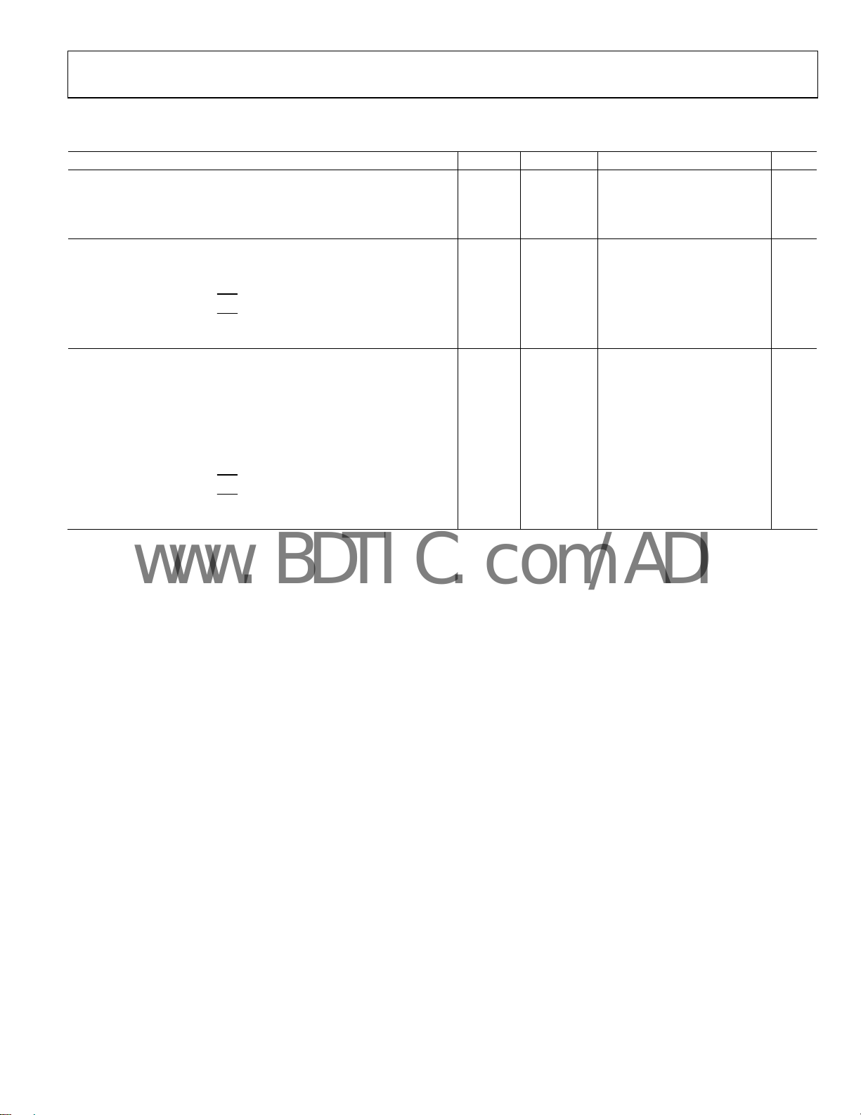
SERIAL PORT TIMING CHARACTERISTICS
Table 9.
Parameter
SERIAL PORT CLOCK TIMING REQUIREMENTS
t
t
t
SPI PORT CONTROL TIMING REQUIREMENTS (MODE = 0)
t
t
t
t
t
SPORT MODE CONTROL TIMING REQUIREMENTS (MODE = 1)
t
t
t
t
t
t
t
t
t
1
All timing specifications are valid over the VDDCORE range of 1.7 V to 1.9 V and the VDDIO range of 3.0 V and 3.6 V.
2
C
LOAD
3
SCLK rise/fall time should be 3 ns maximum.
1, 2, 3
SCLK
SCLKL
SCLKH
SSDI SDI to ↑SCLK Setup Time
HSDI SDI to ↑SCLK Hold Time
SSCS SCS to ↑SCLK Setup Time
HSCS SCS to ↑SCLK Hold Time
DSDO ↑SCLK to SDO Delay Time
SSDI SDI to ↑SCLK Setup Time
HSDI SDI to ↑SCLK Hold Time
SSRFS SRFS to ↓SCLK Setup Time
HSRFS SRFS to ↓SCLK Hold Time
SSTFS STFS to ↓SCLK Setup Time
HSTFS STFS to ↓SCLK Hold Time
SSCS SCS to ↑SCLK Setup Time
HSCS SCS to ↑SCLK Hold Time
DSDO ↑SCLK to SDO Delay Time
= 40 pF on all outputs, unless otherwise noted.
Temp Test Level Min Typ Max Unit
SCLK Period Full IV 10.0 ns
SCLK Low Time Full IV 1.60 0.5 × t
SCLK High Time Full IV 1.60 0.5 × t
SCLK
SCLK
ns
ns
Full IV 1.30 ns
Full IV 0.40 ns
Full IV 4.12 ns
Full IV −2.78 ns
Full IV 4.28 7.96 ns
Full IV 0.80 ns
Full IV 0.40 ns
Full IV 1.60 ns
Full IV −0.13 ns
Full IV 1.60 ns
Full IV −0.30 ns
Full IV 4.12 ns
Full IV −2.76 ns
Full IV 4.29 7.95 ns
Rev. 0 | Page 11 of 88
AD6654
C
K
S
www.BDTIC.com/ADI
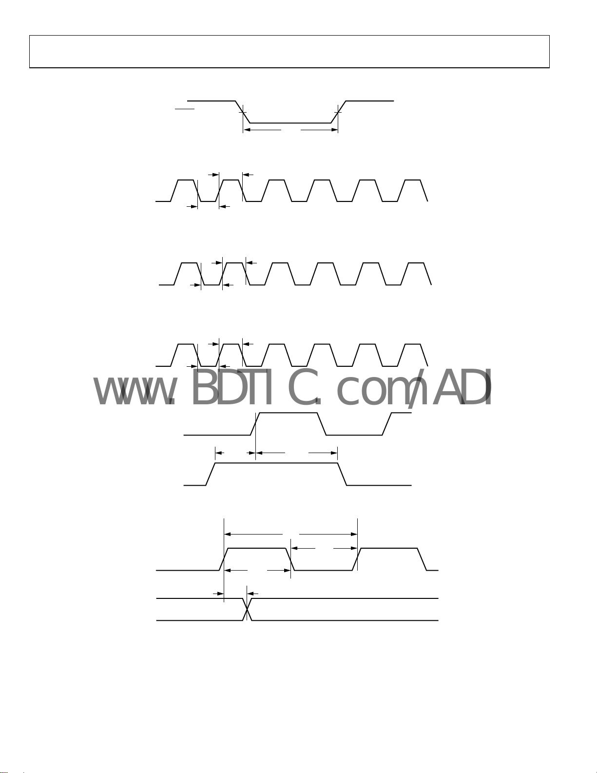
TIMING DIAGRAMS
CLK
PUCL
RESET
t
t
RESL
Figure 2. Reset Timing Requirements
t
CLKH
CLKL
Figure 3. CLK Switching Characteristics
t
CPUCLKH
05156-002
05156-003
SCLK
CLK
CLK
YNC [3:0]
t
CPUCLKL
Figure 4. CPUCLK Switching Characteristics
t
SCLKH
t
SCLKL
Figure 5. SCLK Switching Characteristics
t
SSYNC
t
HSYNC
Figure 6. SYNC Tim ing Inputs
t
CLK
t
CLKH
t
CLKL
05156-006
05156-004
05156-005
t
DEXP
EXPx [2:0]
Figure 7. Gain Control Word Output Switching Characteristics
Rev. 0 | Page 12 of 88
05156-007
AD6654
www.BDTIC.com/ADI
PCLK
PxACK
t
DPREQ
PxREQ
Px [15:0]
t
SPA
t
DPP
I [15:0] Q [15:0]
t
DPP
t
DPP
RSSI [11:0]
t
DPP
I [15:0] Q [15:0]
t
HPA
t
DPP
t
DPP
RSSI [11:0]
PxIQ
PxCH [2:0]
PxGAIN
PCLK
PxACK
PxREQ
Px [15:0]
PxIQ
PxCH [2:0]
PxGAIN
t
DPIQ
t
DPIQ
t
DPCH
PxCH [2:0] = CHANNEL NO.
t
DPGAIN
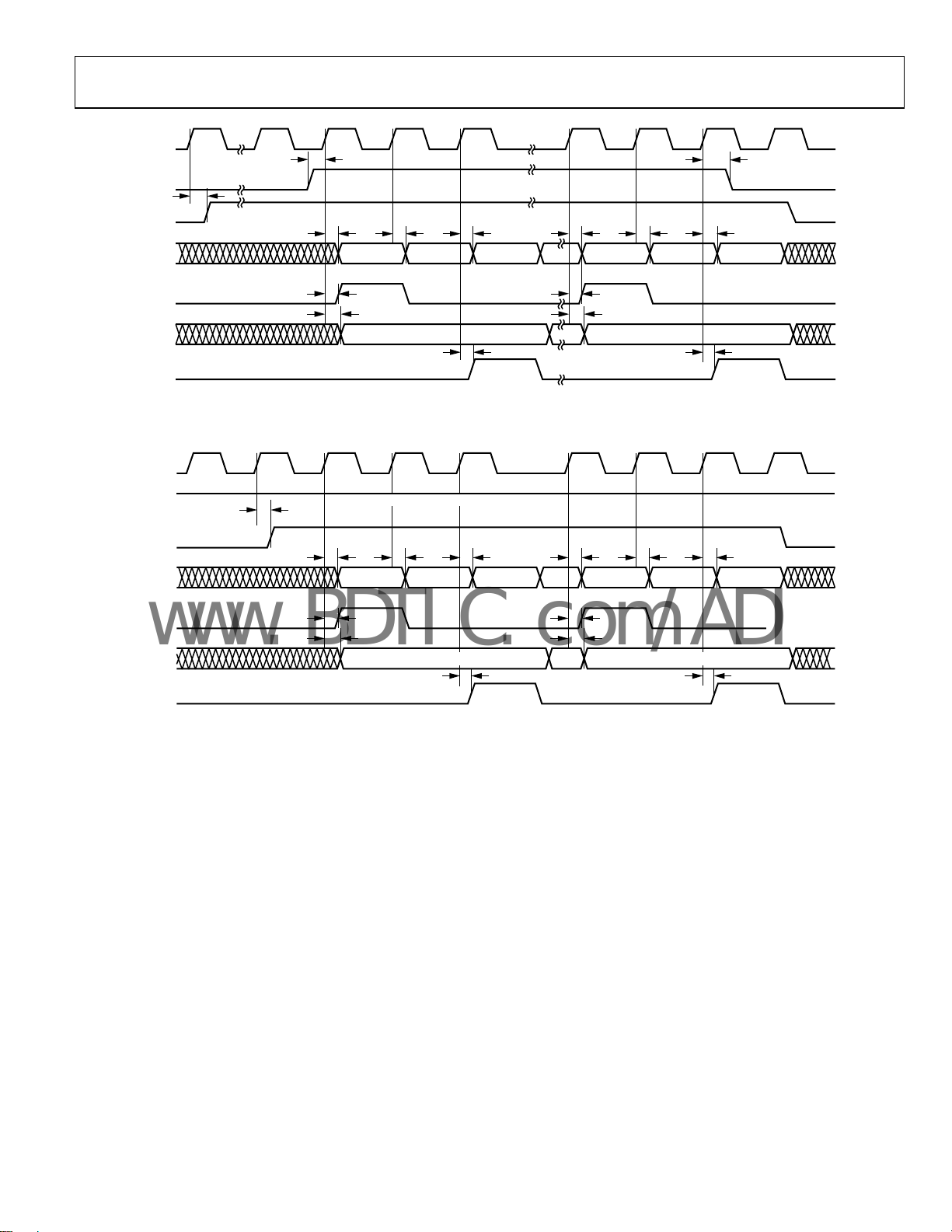
Figure 8. Master Mode PxACK to PCLK Switching Characteristics
t
DPREQ
TIED LOGIC HIGH ALL THE TIME
t
DPP
I [15:0] Q [15:0]
t
DPCH
t
DPP
PxCH [2:0] = CHANNEL NO.
t
DPGAIN
t
DPP
RSSI [11:0] RSSI [11:0]
Figure 9. Master Mode PxREQ to PCLK Switching Characteristics
t
DPIQ
t
DPCH
PxCH [2:0] = CHANNEL NO.
t
DPGAIN
t
DPP
I [15:0] Q [15:0]
t
DPIQ
t
DPCH
t
DPP
PxCH [2:0] = CHANNEL NO.
t
DPGAIN
05156-008
t
DPP
05156-009
Rev. 0 | Page 13 of 88
AD6654
K
t
www.BDTIC.com/ADI
CPUCLK
RD
t
SC
WR
t
SC
CS
t
SAM
A [7:0]
t
SAM
D [15:0]
RDY
NOTE:
t
ACCESS TIME DEPENDS ON THE ADDRESS ACCESSED. IT CAN VARY FROM 3 TO 9 CPUCLK CYCLES.
ACC
t
DRDY
VALID ADDRESS
VALID DATA
t
ACC
t
t
t
HC
HC
HAM
t
HAM
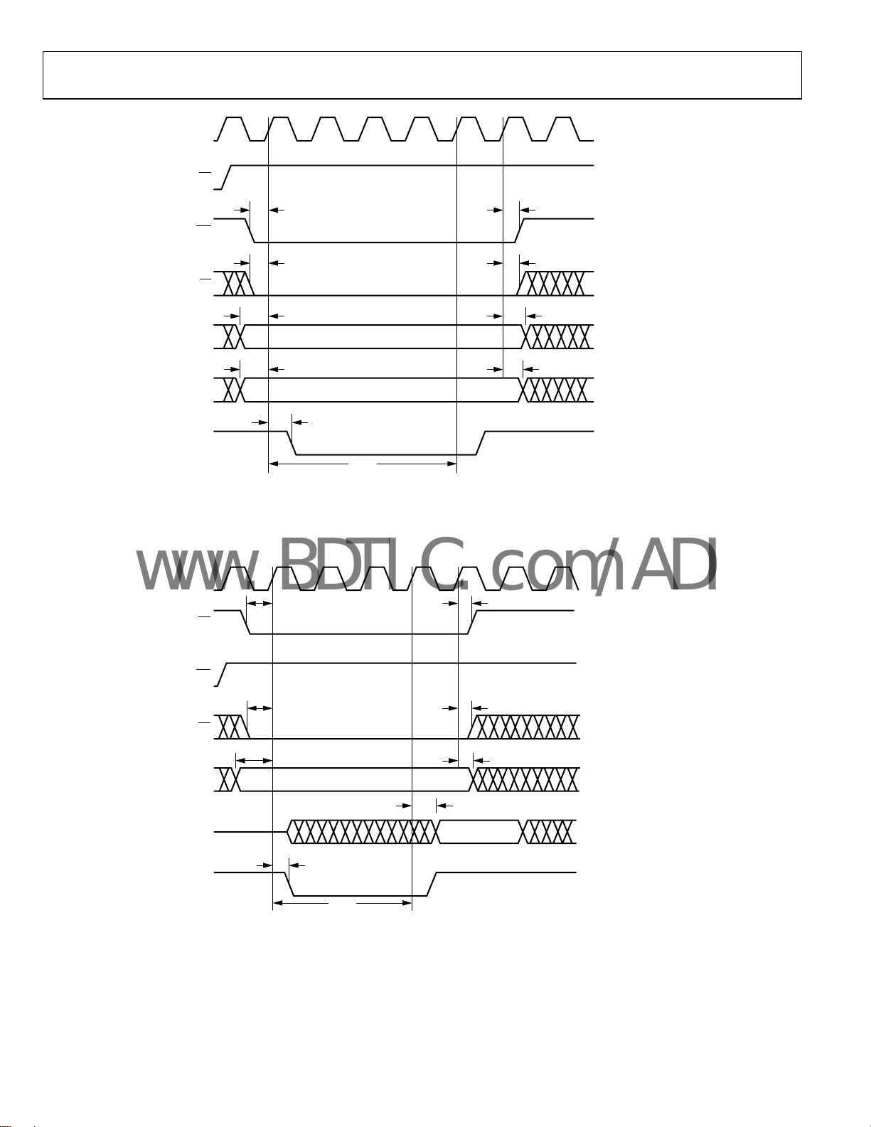
Figure 10. INM Microport Write Timing Requirements
CPUCL
t
HC
RD
t
SC
05156-010
WR
t
t
t
SAM
SC
VALID ADDRESS
t
DRDY
t
ACC
CS
A [7:0]
D [15:0]
RDY
NOTE:
ACCESS TIME DEPENDS ON THE ADDRESS ACCESSED. IT CAN VARY FROM 3 TO 9 CPUCLK CYCLES.
ACC
HC
t
t
DD
VALID DATA
HAM
Figure 11. INM Microport Read Timing Requirements
Rev. 0 | Page 14 of 88
05156-011
AD6654
www.BDTIC.com/ADI
CPUCLK
t
DDTACK
t
t
t
t
HC
HC
HC
HAM
t
HAM
t
SC
DS
t
SC
R/W
t
SC
CS
t
SAM
A [7:0]
t
SAM
D [15:0]
DTACK
NOTE:
t
ACCESS TIME DEPENDS ON THE ADDRESS ACCESSED. IT CAN VARY FROM 3 TO 9 CPUCLK CYCLES.
ACC
VALID ADDRESS
VALID DATA
t
ACC
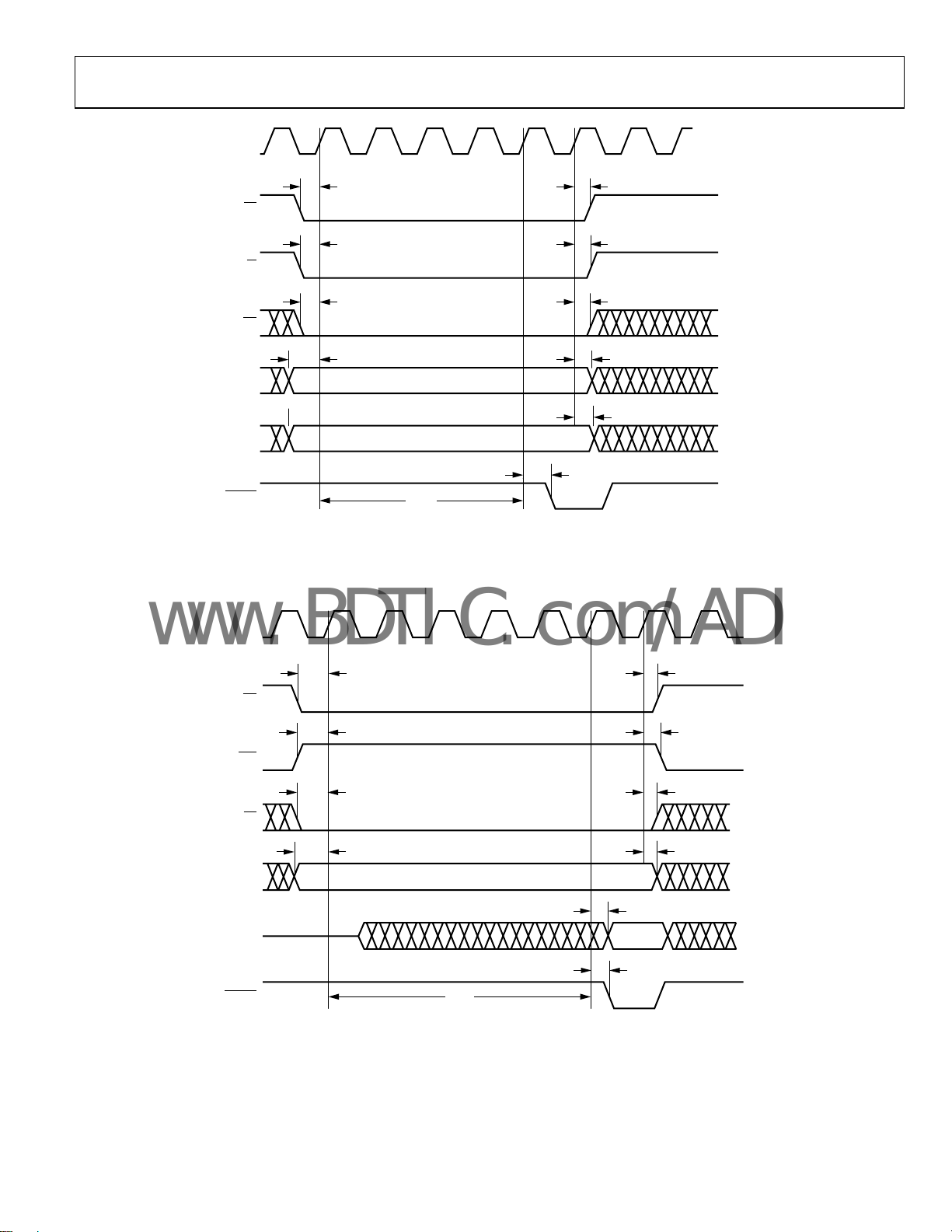
Figure 12. MNM Microport Write Timing Requirements
CPUCLK
05156-012
t
SC
DS
t
SC
R/W
t
SC
CS
t
SAM
A [7:0]
D [15:0]
DTACK
NOTE:
t
ACCESS TIME DEPENDS ON THE ADDRESS ACCESSED. IT CAN VARY FROM 3 TO 9 CPUCLK CYCLES.
ACC
VALID ADDRESS
t
ACC
t
DD
VALID
DATA
t
DDTACK
Figure 13. MNM Microport Read Timing Requirements
t
t
t
HC
t
HC
HC
HAM
05156-013
Rev. 0 | Page 15 of 88
AD6654
www.BDTIC.com/ADI
SCLK
SCS
t
SSCS
t
HSCS
SMODE
SDI
SRFS
MODE
SCLK
SCS
SMODE
SDO
STFS
t
SSCS
t
SSRFS
t
SSTFS
t
SSDI
t
HSDI
D0 D1 D2 D3 D4 D5 D6 D7
t
HSRFS
LOGIC 1
LOGIC 1
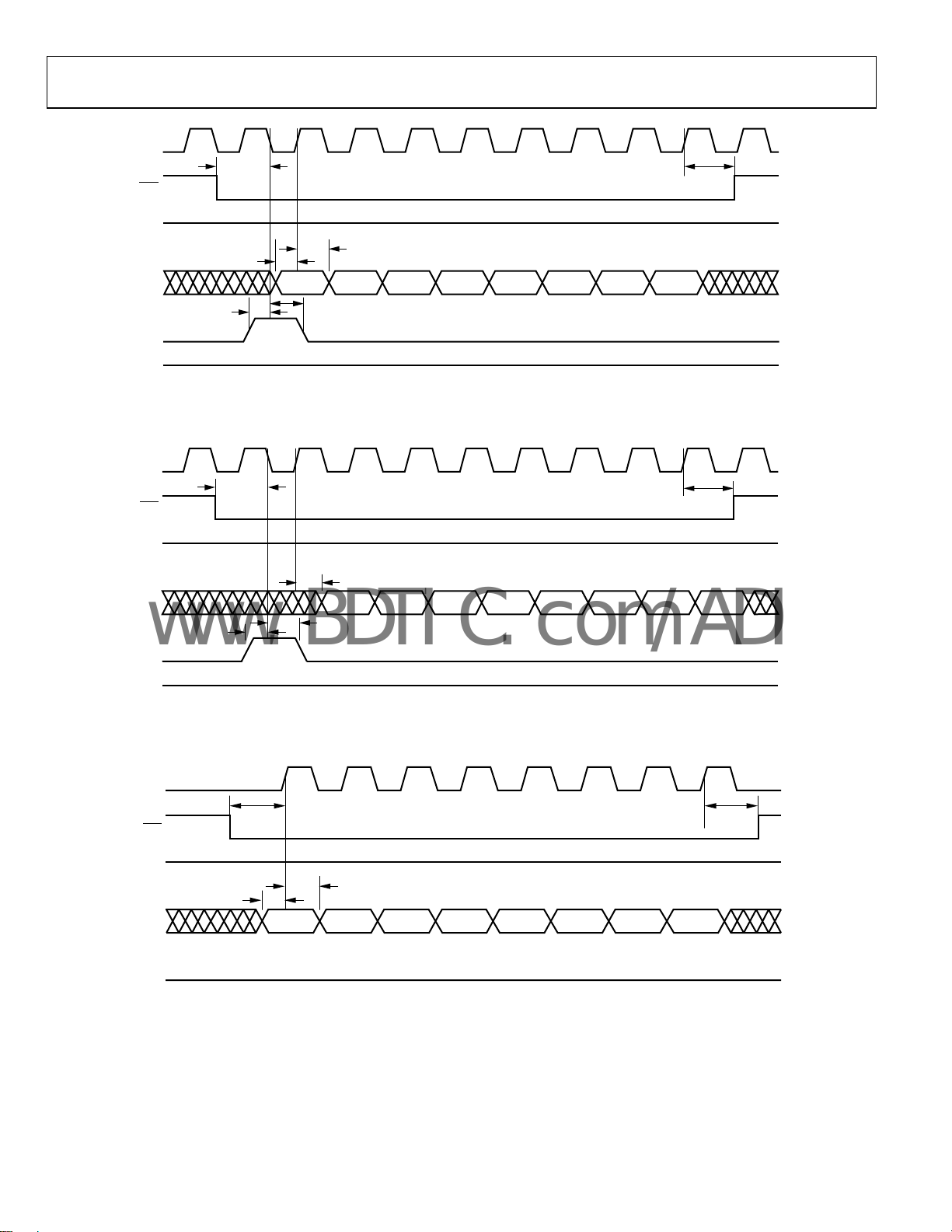
Figure 14. SPORT Mode Write Timing Characteristics
LOGIC 1
t
DSDO
D0 D1 D2 D3 D4 D5 D6 D7
t
HSTFS
t
HSCS
05156-014
MODE
SCLK
SCS
SMODE
SDI
MODE
t
SSDI
LOGIC 1
Figure 15. SPORT Mode Read Timing Characteristics
t
SSCS
t
HSDI
D0 D1 D2 D3 D4 D5 D6 D7
LOGIC 1
LOGIC 0
Figure 16. SPI Mode Write Timing Characteristics
t
HSCS
05156-015
05156-016
Rev. 0 | Page 16 of 88
AD6654
www.BDTIC.com/ADI
SCLK
SCS
SMODE
SDO
MODE
t
SSCS
t
HSCS
LOGIC 0
t
DSDO
D0 D1 D2 D3 D4 D5 D6 D7
LOGIC 0
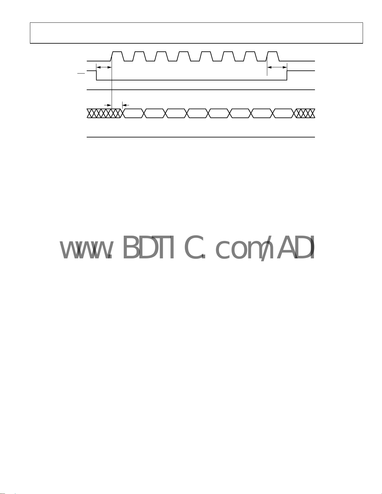
Figure 17. SPI Mode Read Timing Characteristics
05156-017
Rev. 0 | Page 17 of 88

AD6654
www.BDTIC.com/ADI
ABSOLUTE MAXIMUM RATINGS
Table 10.
Parameter Rating
AVDD 0 to +7.0 V
DRVDD 0 to +4.0 V
VDDCORE −0.3 V to +2.2 V
VDDIO 0 to +4.0 V
Analog/Encode Input Voltage 0 to AVDD
Analog Input Current 25 mA
Digital Input Voltage
Digital Output Voltage −0.3 V to VDDIO + 0.3 V
Operating Temperature Range
(Ambient)
Junction Temperature Under Bias 150°C
Storage Temperature Range −65°C to +150°C
−0.3 V to + 3.6 V (not 5 V
tolerant)
−25°C to +85°C
Stresses above those listed under Absolute Maximum Ratings
may cause permanent damage to the device. This is a stress
rating only; functional operation of the device at these or any
other conditions above those indicated in the operational
section of this specification is not implied. Exposure to absolute
maximum rating conditions for extended periods may affect
device reliability.
THERMAL CHARACTERISTICS
256 BGA, 17 mm sq.
= 21°C/W, no airflow.
θ
JA
Estimate based on JEDEC JC51-2 model using horizontally
positioned 4-layer board.
EXPLANATION OF TEST LEVELS
Test Level Description
I 100% production tested.
II 100% production tested at 25°C.
III Sample tested only.
IV Parameter guaranteed by design and analysis.
V Parameter is typical value only.
ESD CAUTION
ESD (electrostatic discharge) sensitive device. Electrostatic charges as high as 4000 V readily accumulate on
the human body and test equipment and can discharge without detection. Although this product features
proprietary ESD protection circuitry, permanent damage may occur on devices subjected to high energy
electrostatic discharges. Therefore, proper ESD precautions are recommended to avoid performance
degradation or loss of functionality.
Rev. 0 | Page 18 of 88
AD6654
www.BDTIC.com/ADI
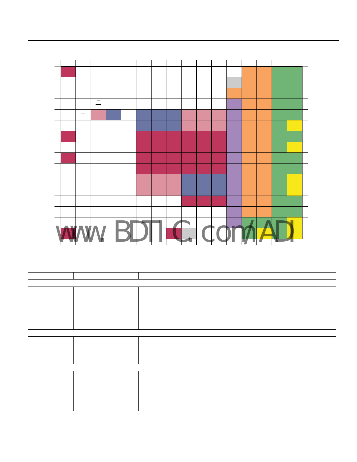
PIN CONFIGURATION AND FUNCTION DESCRIPTIONS
12345678910111213141516
DTACK
(RDY,
SDO)
CS
(SCS)
CPUCLK
PC3 PCCH1 PA12 PAIQ PAGAIN PB6 CLK OVR AVDD AVDD AGND AGND A
(SCLK)
DS
PC5 PA5 PA15 PAACK PB2 PB4 EXPC2 DNC AVDD AVDD AGND AGND B
(RD,
SRFS)
R/W
PC0 PA3 PA9 PACH2 PB9 EXPC1 AVDD AVDD AVDD AGND AGND C
(WR,
STFS)
PC6 PC2 PA1 PA7 PACH0 PB15 EXPC0 DRVDD AVDD AVDD AGND AGND D
VDD
CORE
PCACK
VDD
CORE
VDD
CORE
VDD
CORE
VDD
CORE
VDD
CORE
VDD
CORE
PB3
PB0
VDDIO VDDIO DRVDD AVDD AVDD AGND AGND E
VDDIO
VDDIO VDDIO DRVDD AVDD AVDD AGND C2 F
VDDIO
A DGND D14 D12
B D7 CHIPID3 CHIPID2
C CHIPID0 MODE
_
MSB
FIRST
_
EXT
D
FILTER
E CHIPID1 IRP VDDIO
F SMODE D13 D15 RESET D1
G DGND D8 D9 D2 D5 DGND DGND DGND DGND DGND DGND DRVDD AVDD AVDD AGND AGND G
H D3 D11 D4 D10 A6 DGND DGND DGND DGND DGND DGND DRVDD AVDD AVDD AGND C1 H
J DGND D6 D0 A7 A1 DGND DGND DGND DGND DGND DGND DRVDD AVDD AVDD AGND AGND J
K A5 A0 (SDI) A2 PC8 DGND DGND DGND DGND DGND DGND DRVDD AVDD AVDD AGND AGND K
L A3 PC11 PC15 PC10 VDDIO VDDIO VDDIO
M PC14 PC13 PC9 PC7 PCCH0 VDDIO VDDIO VDDIO
N PC1 PC4 PA13 PA8 PA0 PAREQ PB1 PB REQ DGND DGND DGND DRVDD AVDD AVDD AGND AGND N
P PCIQ PCREQ PA14 PA10 PB10 PB7 PB8 PBCH1 PBACK PBCH0 SYNC2 DRVDD AVDD AVDD AGND AGND P
R PCCH2 PCGAIN PA6 PA2 PACH1 PB13 PB11 PBCH2 PB14 PBGAIN SYNC1 DRVDD AGND AGND AGND ENC–R
T DGND PA11 PA4 PCLK PB5 PB12 PBIQ DGND DNC SYNC0 SYNC3 DR AGND V
DNC = DO NOT CONNECT
A4
VDD
VDD
VDD
PC12
12345678910111213141516
CORE
VDD
CORE
CORE
VDD
CORE
DRVDD AVDD AVDD AGND AIN–L
CORE
VDD
DRVDD AVDD AVDD AGND AIN+ M
CORE
REF
AGND ENC+ T
05156-018
Figure 18. 256 BGA Configuration (Top View)
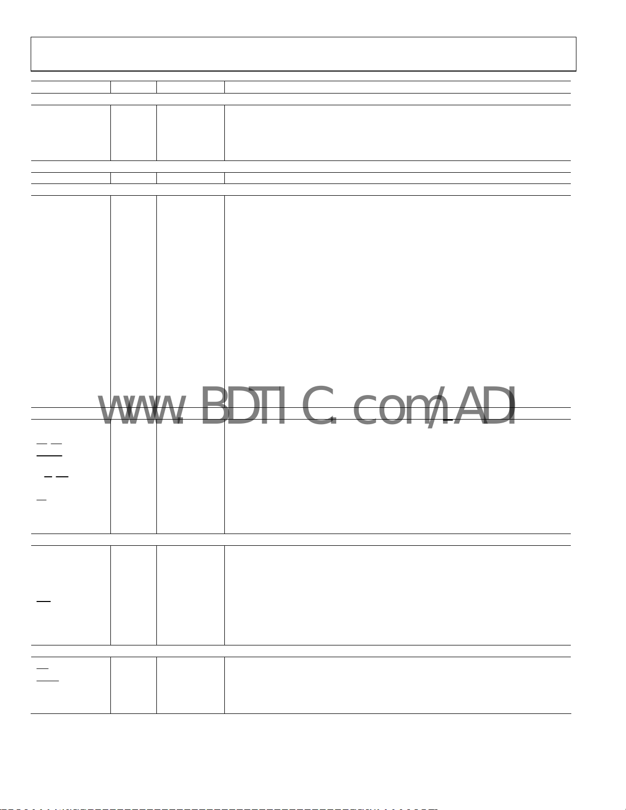
Table 11. Pin Function Descriptions
Name Type Pin Number Function
POWER SUPPLY
AVDD Power
DRVDD Power
VDDCORE Power
VDDIO Power
DGND Ground
AGND Ground
See
See
See
See
See
See
Table 12
Table 12
Table 12
Table 12
Table 12
Table 12
ADC INPUTS
AIN+ Input M16 Differential Analog Input.
AIN− Input L16 Differential Analog Input.
ENC+ Input T16 Differential Encode Input. Conversion initiated on rising edge.
ENC− Input R16 Differential Encode Input.
ADC OUTPUTS
DR Output T12 Data Ready. Inverted and delayed representation of ENC+ used for driving the DDC CLK
OVR Output A12 Overange Bit. A logic high indicates analog input exceeds ±FS.
V
Output T14 2.4 V Fixed Internal Voltage Reference. Bypass to AGND with 0.1 µF chip capacitor.
REF
C1 Output H16 Compensation Pin for ADC Voltage Reference. Bypass to AGND with 0.1 µF chip capacitor.
C2 Output F16 Compensation Pin for ADC Voltage Reference. Bypass to AGND with 0.1 µF chip capacitor.
5 V Analog ADC Core Supply.
3.3 V ADC Output Driver Supply.
1.8 V Digital DDC Core Supply.
3.3 V Digital DDC I/O Supply.
Digital Core and I/O Ground.
Analog ADC Ground.
input.
Rev. 0 | Page 19 of 88
AD6654
www.BDTIC.com/ADI
Name Type Pin Number Function
DDC INPUTS
CLK Input A11 DDC Clock Input.
SYNC0 Input T10 Synchronization Input 0. SYNC pins are independent of channels.
SYNC1 Input R11 Synchronization Input 1.
SYNC2 Input P11 Synchronization Input 2.
SYNC3 Input T11 Synchronization Input 3.
DDC OUTPUTS
EXPC [2:0] Output D11, C11, B11 External VGA Gain Control Bits. GND all pins if not used.
DDC OUTPUT PORTS
PCLK Bi-dir T4 Parallel Output Port Clock. PCLK is bi-directional: master mode = output, slave mode = input.
PADATA[15:0] Output
PACH[2:0] Output D8, R5, C8 Channel Indicator Output Port A.
PAIQ Output A8 Parallel Port A I/Q Data Indicator. Logic 1 indicates I data on data bus.
PAGAIN Output A9 Parallel Port A Gain Word Output Indicator. Logic 1 indicates gain word on data bus.
PAACK Input B8 Parallel Port A Acknowledge (Active High).
PAREQ Output N6 Parallel Port A Request (Active High).
PBDATA[15:0] Output
PBCH[2:0] Output P10, P8, R8 Channel Indicator Output Port B.
PBIQ Output T7 Parallel Port B I/Q Data Indicator. Logic 1 indicates I data on data bus.
PBGAIN Output R10 Parallel Port B Gain Word Output Indicator. Logic 1 indicates gain word on data bus.
PBACK Input P9 Parallel Port B Acknowledge (Active High).
PBREQ Output N8 Parallel Port B Request (Active High)
PCDATA[15:0] Output
PCCH[2:0] Output M5, A6, R1 Channel Indicator Output Port C.
PCIQ Output P1 Parallel Port C I/Q Data Indicator. Logic 1 indicates I data on data bus.
PCGAIN Output R2 Parallel Port C Gain word Output Indicator. Logic 1 indicates gain word on data bus.
PCACK Input E5 Parallel Port C Acknowledge (Active High).
PCREQ Output P2 Parallel Port C Request (Active High).
MICROPORT CONTROL
D[15:0] Bi-Dir
A[7:0] Input
DS
(RD)
DTACK
(RDY)1
R/W (WR)
MODE Input C2 Mode Select. Logic 0 = Intel® mode, Logic 1 = Motorola mode.
CS
CPUCLK Input A4 Microport CLK Input. (Input only.)
CHIPID[3:0] Input C1, E1, B3, B2 Chip ID Input Pins.
SERIAL PORT CONTROL
SCLK Input A4 Serial Clock. Should have a rise/fall time of 3ns max.
1
SDO
SDI2 Input K3 Serial Port Data Input.
STFS Input C4 Serial Transmit Frame Sync.
SRFS Input B4 Serial Receive Frame Sync.
SCS Input D3 Serial Chip Select.
MSB_FIRST Input D2 Most Significant Bit_First. Selects MSB_FIRST into SDI pin, and MSB_FIRST out of SDO pin.
SMODE Input F1 Serial Mode Select.
MISC PINS
DNC ------- B12, T9 Do Not Connect.
1
IRP
RESET Input F4 Master Reset, Active Low.
EXT_FILTER Input D1 PLL Loop Filter (Analog Pin). Connect to VDDCORE through series 250 Ω and 0.01 µF
1
Pins with internal pull-up resistor of nominal 70 kΩ.
2
Pins with internal pull-down resistor of nominal 70 kΩ.
Input B4 Active Low Data Strobe, MODE = 1. Active lo
Output C3 Active Low Data Acknowledge, MODE = 1. Micro
Input C4 Read/Write Strobe, MODE = 1. Ac
Input D3 Active Low Chip Select. Logic 1 th
Output C3 Serial Port Data Output. Terminate to VDDIO through external 1 kΩ pull-up resistor.
Output E2 Interrupt Pin (Active Low). Terminate to VDDIO through external 1 kΩ pull-up resistor.
See
See
See
See
See
Table 12
Table 12
Table 12
Table 12
Table 12
Parallel Output Port A Data Bus.
Parallel Output Port B Data Bus.
Parallel Output Port C Data Bus.
Bidirectional Microport Data. This bus is three-stated when
Microport Address Bus.
w read strobe when MODE = 0.
port status pin when MODE = 0. Terminate
to VDDIO through external 1 kΩ pull-up resistor.
tive low write strobe when MODE = 0.
ree-states the microport data bus.
Logic 1 = MSB_FIRST; Logic 0 = LSB_FIRST
capacitor.
CS
is high.
Rev. 0 | Page 20 of 88

AD6654
www.BDTIC.com/ADI
Table 12. Pin Listing for Power, Ground, and Data Buses
Name Pin Number
AVDD
AGND
DRVDD D12, E12, F12, G12, H12, J12, K12, L12, M12, N12, P12, R12
VDDIO E3, E9, E10, E11, F9, F10, F11, L6, L7, L8, M6, M7, M8
VDDCORE E4, E6, E7, E8, F6, F7, F8, L9, L10, L11, M9, M10, M11
DGND
PADATA[15:0] N5, D6, R4, C6,T3, B6, R3, D7, N4, C7, P4, T2, A7, N3, P3, B7
PBDATA[15:0] D9, N7, B9, C9, B10, T5, A10, P6, P7, C10, P5, R7, T6, R6, R9, D10
PCDATA[15:0] C5, N1, D5, A5, N2, B5, D4, M4, K5, M3, L5, L3, L2, M2, M1, L4
D[15:0] J3, F5, G4, H1, H3, G5, J2, B1, G2, G3, H4, H2, A3, F2, A2, F3
A[7:0] K3, J5, K4, L1, K2, K1, H5, J4
A13, A14, B13, B14, C12, C13, C14, D13, D14, E13, E14, F13, F14,
M14, N13, N14, P13, P14
A15, A16, B15, B16, C15, C16, D15, D16, E15, E16, F15, G15, G16,
R13, R14, R15, T13, T15
A1, G1, G6, G7, G8, G9, G10, G11, H6, H7, H8, H9, H10, H11, J1, J6, J7, J8, J9, J10, J11, K6, K7, K8, K9, K10, K11, N9, N10,
N11, T1,
T8
G13, G14, H13, H14, J13, J14, K13, K14, L13, L14, M13,
H15, J15, J16, K15, K16, L15, M15, N15, N16, P15, P16,
Rev. 0 | Page 21 of 88
AD6654
www.BDTIC.com/ADI
TYPICAL PERFORMANCE CHARACTERISTICS
76
75
+25°C
74
73
SNR (dB)
72
71
ENCODE = 92.16MSPS
AIN = –1dBFS
70
10
30 50 70 90 110 130 150 170 190
+85°C
AIN FREQUENCY (MHz)
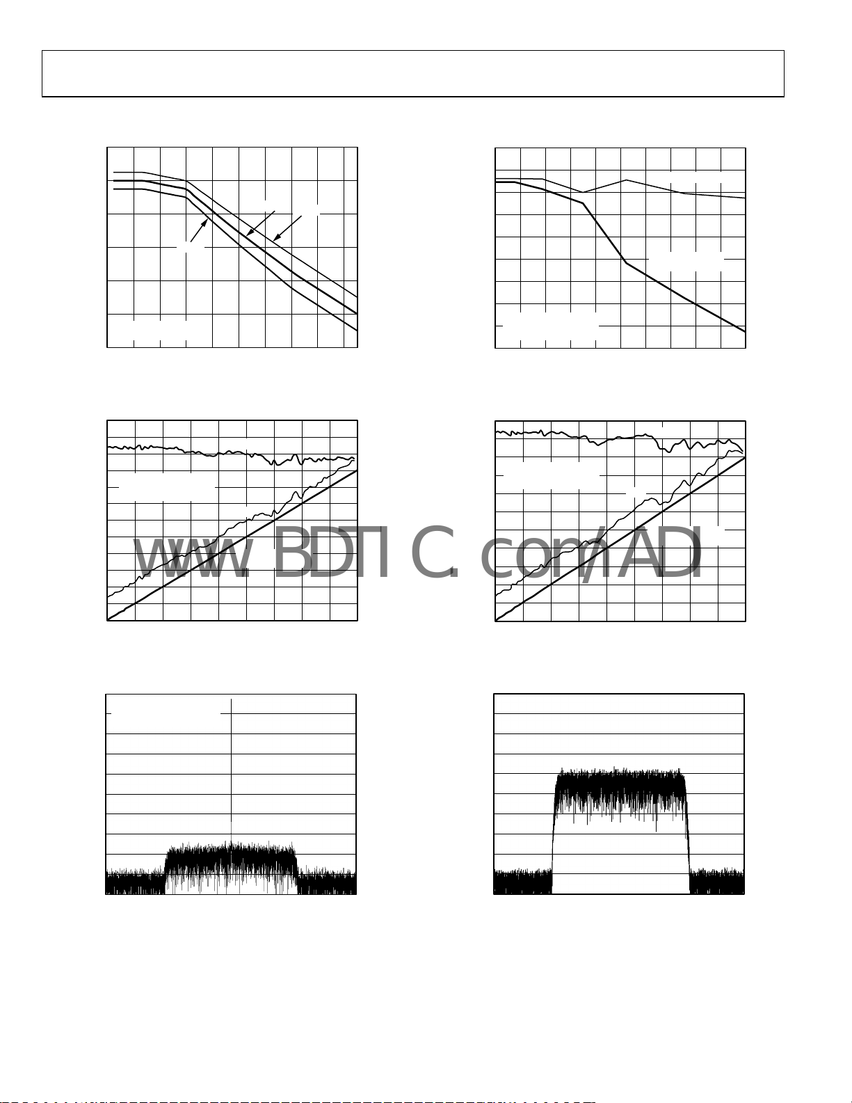
Figure 19. ADC Noise vs. Analog Frequency (46.08 MHz BW)
–25°C
05156-073
105
100
95
90
85
80
75
70
WORST CASE HARMONIC (dBc)
ENCODE = 92.16MSPS
65
AIN = –1dBFS
TEMPERATURE = 25
60
200 40 60 80 100 120 140 160 180 200
°
C
ANALOG INPUT FREQUENCY (MHz)
WORST OTHER SPUR
HARMONICS
(SECOND, THIRD)
05156-074
Figure 22. Harmonics vs. Analog Frequency (IF)
120
110
100
90
ENCODE = 92.16MSPS
AIN = 37.7MHz
80
TEMPERATURE = 25°C
70
60
50
40
30
20
WORST CASE SPURIOUS (dBFS and dBc)
10
0
–80 –70 –60 –50 –40 –30 –20 –10
ANALOG INPUT POWER LEVEL (dBFS)
dBFS
dBc
SFDR = 90dB
REFERENCE LINE
Figure 20. Single Tone SFDR at 37.7 MHz
0
AIN = –1dBFS
SNR = 89dB (1.25MHz BW)
–15
32k FFT
–30
–45
–60
–75
(dBFS)
–90
–105
–120
–135
–150
–1.25M
–1.00M
–750k
–500k
0
–250k
FREQUENCY (Hz)
250k
500k
750k
Figure 21. CDMA Single Tone AIN = 70 MHz; ENC = 92.16 MSPS
1.00M
0–90
1.25M
05156-071
05156-064
110
100
90
ENCODE = 92.16MSPS
80
AIN = 70MHz
TEMPERATURE = 25
70
60
50
40
30
20
WORST CASE SPURIOUS (dBFS and dBc)
10
0
–80 –70 –60 –50 –40 –30 –20 –10
ANALOG INPUT POWER LEVEL (dBFS)
°
C
dBFS
dBc
SFDR = 90dB
REFERENCE LINE
Figure 23. Single Tone SFDR at 70 MHz
0
32k FFT
–15
–30
–45
–60
–75
(dBFS)
–90
–105
–120
–135
–150
–1.25M
–1.00M
–750k
–500k
0
–250k
FREQUENCY (Hz)
250k
500k
Figure 24. CDMA Carrier AIN = 70 MHz; ENC = 92.16 MSPS
750k
1.00M
0–90
1.25M
05156-072
05156-066
Rev. 0 | Page 22 of 88
AD6654
www.BDTIC.com/ADI
0
AIN = –1dBFS
–15
SNR = 88dB (1.25MHz BW)
32k FFT
–30
–45
–60
–75
(dBFS)
–90
–105
–120
–135
–150
–1.25M
–1.00M
–750k
–500k
0
–250k
FREQUENCY (Hz)
250k
500k
750k
1.00M
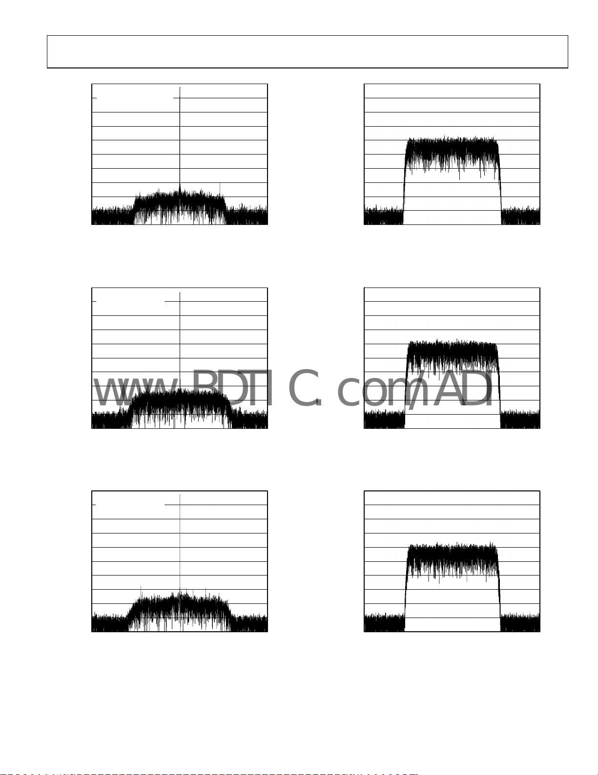
Figure 25. CDMA Single Tone AIN = 151.5 MHz; ENC = 92.16 MSPS
05156-065
1.25M
0
32k FFT
–15
–30
–45
–60
–75
(dBFS)
–90
–105
–120
–135
–150
–1.25M
–1.00M
–750k
–500k
0
–250k
FREQUENCY (Hz)
250k
500k
750k
Figure 28. CDMA Carrier AIN = 151.5 MHz; ENC = 92.16 MSPS
1.00M
05156-083
1.25M
0
AIN = –1dBFS
SNR = 83dB (5MHz BW)
–15
32k FFT
–30
–45
–60
–75
(dBFS)
–90
–105
–120
–135
–150
–3.5M
–2.8M
–2.1M
–1.4M
0
–700k
FREQUENCY (Hz)
700k
1.4M
2.1M
2.8M
3.5M
Figure 26. WCDMA Single Tone AIN = 70 MHz; Encode = 92.16 MSPS
0
AIN = –1dBFS
SNR = 82dB (5MHz BW)
–15
32k FFT
–30
–45
–60
–75
(dBFS)
–90
–105
–120
–135
–150
–3.5M
–2.8M
–2.1M
–1.4M
0
–700k
FREQUENCY (Hz)
700k
1.4M
2.1M
2.8M
3.5M
Figure 27. WCDMA Single Tone AIN = 151.5 MHz; Encode = 92.16 MSPS
05156-067
05156-068
0
32k FFT
–15
–30
–45
–60
–75
(dBFS)
–90
–105
–120
–135
–150
–3.5M
–2.8M
–2.1M
–1.4M
0
–700k
FREQUENCY (Hz)
700k
1.4M
2.1M
2.8M
3.5M
Figure 29. WCDMA Carrier AIN = 70 MHz; Encode = 92.16 MSPS
0
32k FFT
–15
–30
–45
–60
–75
(dBFS)
–90
–105
–120
–135
–150
–3.5M
–2.8M
–2.1M
–1.4M
0
–700k
FREQUENCY (Hz)
700k
1.4M
2.1M
2.8M
3.5M
Figure 30. WCDMA Carrier AIN = 151.5 MHz; Encode = 92.16 MSPS
05156-069
05156-084
Rev. 0 | Page 23 of 88
AD6654
www.BDTIC.com/ADI
0
AIN = –7dBFS
–15
32k FFT
–30
–45
–60
–75
(dBFS)
–90
–105
–120
–135
–150
–1.25M
–1.00M
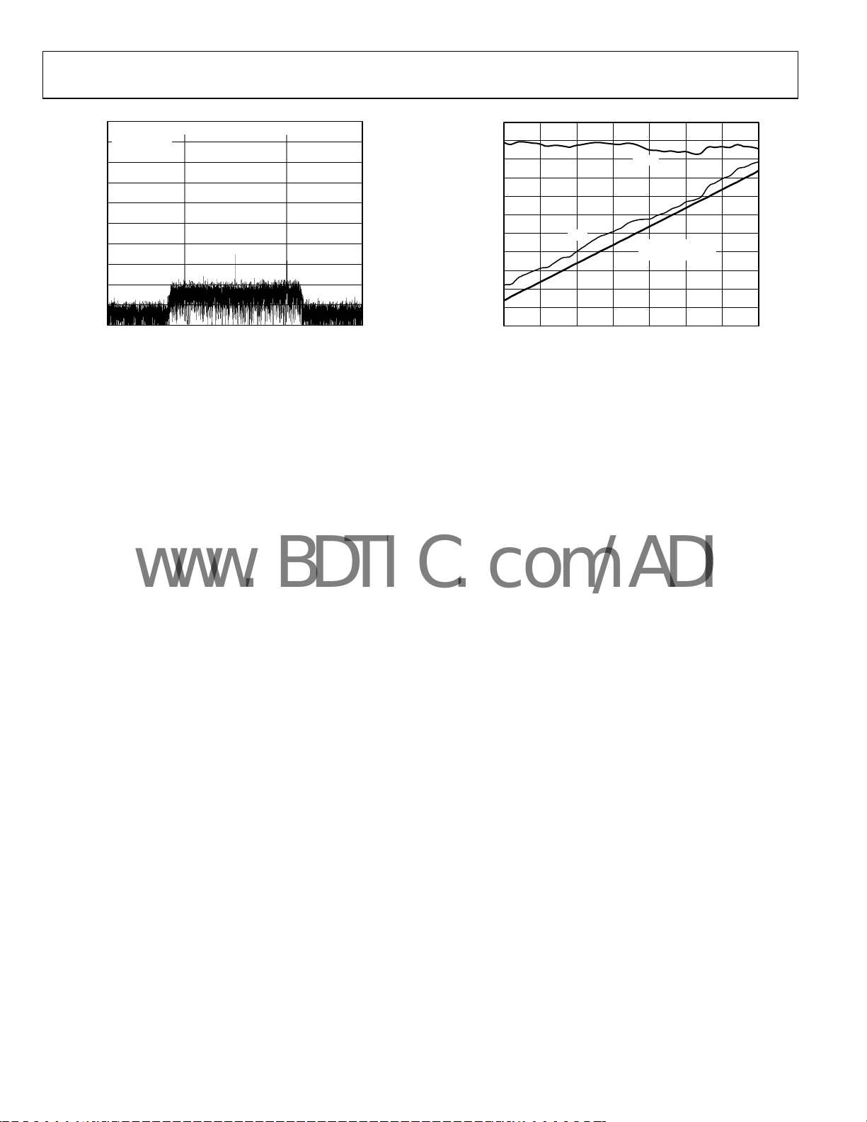
Figure 31. CDMA Two Tones at 55 MHz and 56 MHz; ENC = 92.16 MSPS
F1 F2
–750k
–500k
–250k
FREQUENCY (Hz)
0
250k
500k
750k
1.00M
05156-063
1.25M
110
100
90
80
70
60
50
40
30
20
WORST CASE SPURIOUS (dBFS and dBc)
10
0
dBc
–67 –57 –47 –37 –27 –17
INPUT POWER LEVEL (F1 = F2 (dBFS))
dBFS
SFDR = 90dB
REFERENCE LINE
–7–77
05156-070
Figure 32. Two Tone SFDR at 55 MHz and 56 MHz
Rev. 0 | Page 24 of 88
AD6654
A
A
www.BDTIC.com/ADI
ADC EQUIVALENT CIRCUITS
ENC+
AVDD
2.4V
100µA
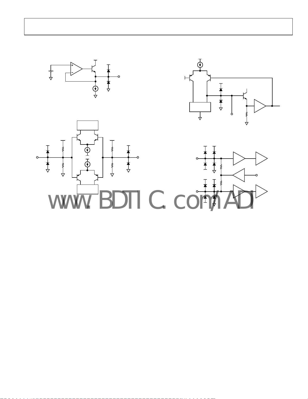
Figure 33. ADC 2.4 V Reference
LOADS
AVDD
10kΩ
10kΩ
LOADS
Figure 34. ADC Encode Inputs
AVDD
AVDD
AVDD
10kΩ
10kΩ
V
REF
AVDD
05156-023
ENC–
05156-024
AVDD
V
REF
CURRENT
MIRROR
AVDD
C1, C2
AVDD
05156-025
Figure 35. ADC Compensation Pins, C1 and C2
V
AVDD
CH
IN+
IN–
BUF
AVDD
500Ω
BUF
500Ω
BUF
V
CL
V
CH
V
CL
T/H
T/H
V
REF
05156-026
Figure 36. ADC Analog Input Stage
Rev. 0 | Page 25 of 88

AD6654
www.BDTIC.com/ADI
TERMINOLOGY
Analog Bandwidth
The analog input frequency at which the spectral power of the
fundamental frequency (as determined by the FFT analysis) is
reduced by 3 dB.
Differential Analog Input Resistance,
Capacitance, and Impedance
The real and complex impedances measured at each analog
input port. The resistance is measured statically, and the
capacitance and differential input impedances are measured
with a network analyzer.
Differential Analog Input Voltage Range
The peak-to-peak differential voltage that must be applied to
the converter to generate a full-scale response. Peak differential
voltage is computed by observing the voltage on a single pin
and subtracting the voltage from the other pin, which is 180°
out of phase. Peak-to-peak differential is computed by rotating
the inputs phase 180° and taking the peak measurement again.
Then the difference is computed between both peak
measurements.
Encode Pulse Width/Duty Cycle
Pulse width high is the minimum amount of time that the
ENCODE pulse should be left in Logic 1 state to achieve the
rated performance. Pulse width low is the minimum time
ENCODE pulse should be left in the low state. Several internal
timing parameters are a function of t
performance will be achieved with 50/50 duty cycle.
Harmonic Distortion, Second
The ratio of the rms signal amplitude to the rms value of the
second harmonic component, reported in dBc.
Harmonic Distortion, Third
The ratio of the rms signal amplitude to the rms value of the
third harmonic component, reported in dBc.
Full-Scale Input Power
Expressed in dBm. Computed using the following equation:
⎛
⎜
⎜
Power
=
SCALEFULL
⎜
log10
⎜
⎜
⎜
⎝
Minimum Conversion Rate
The encode rate at which the SNR of the lowest analog signal
frequency drops by no more than 3 dB below the guaranteed
limit.
Maximum Conversion Rate
Encode rate at which parametric testing is performed.
and t
ENCL
2
V
Z
SCALEFULL
INPUT
001.0
, optimum
ENCH
RMS
⎞
⎟
⎟
⎟
⎟
⎟
⎟
⎠
Noise for Any Range Within the ADC
−−
⎛
⎜
⎝
×=
10
NOISE
Z is the input impedance, FS is the full scale of the device
where
for the frequency in question,
input level, and
ZV
SNR is the value for the particular
SIGNAL is the signal level within the ADC
SIGNALSNRFS
10
⎞
dBFSdBcdBm
⎟
⎠
reported in dB below full scale. This value includes both
thermal and quantization noise.
Power-Supply Rejection Ratio
The ratio of a change in input offset voltage to a change in
power-supply voltage.
Power-Supply Rise Time
The time from when the dc supply is initiated until the supply
output reaches the minimum specified operating voltage for the
AD6654, measured at the supply pin(s) of the AD6654.
Processing Gain
When the tuned channel occupies less bandwidth than the
input signal, this rejection of out-of-band noise is referred to as
processing gain. By using large decimation factors, processing
gain can improve the SNR of the ADC by 15 dB or more. Use
the following equation to estimate processing gain:
GainProcessing
log10_
⎢
⎣
⎡
=
RateSample
BandwidthFilter
_
⎤
2/_
⎥
⎦
Signal-to-Noise Ratio (Without Harmonics)
The ratio of the rms signal amplitude (set at 1 dB below full
scale) to the rms value of the sum of all other spectral
components, excluding the first five harmonics and dc.
Spurious-Free Dynamic Range (SFDR)
The ratio of the rms signal amplitude to the rms value of the
peak spurious spectral component. The peak spurious component might, or might not be, a harmonic. SFDR can be reported
in dBc (degrades as signal level is lowered), or dBFS (always
related back to converter full scale).
Two-Tone Intermodulation Distortion Rejection
The ratio of the rms value of either input tone to the rms value
of the worst third-order intermodulation product, in dBc.
Two -Tone SFDR
Ratio of the rms value of either input tone to the rms value of
the peak spurious component. The peak spurious component
might, or might not be, an IMD product. SFDR can be reported
in dBc (degrades as signal level is lowered), or in dBFS (always
related back to converter full scale).
Worst Other Spur
Ratio of the rms signal amplitude to the rms value of the worst
spurious component (excluding the second and third harmonic)
reported in dBc.
Rev. 0 | Page 26 of 88

AD6654
www.BDTIC.com/ADI
THEORY OF OPERATION
ADC ARCHITECTURE
The AD6654 analog-to-digital converter (ADC) front end
employs a 3-stage subrange architecture. This design approach
achieves the required accuracy and speed, while maintaining
low power consumption.
The AD6654 front end has complementary analog input pins,
AIN+ an
centered at 2.4 V and should swing ±0.55 V around this
reference (see Figure 36). Because AIN+ and AIN− are 180°
out of phase, the differential full-scale analog input signal is
2.2 V p-p.
Both analog inputs are buffered prior to the first track-andh
hold mode. The held value of TH1 is applied to the input of a
5-bit coarse ADC1. The digital output of ADC1 drives a 5-bit
digital-to-analog converter, DAC1. DAC1 requires 14 bits of
precision that is achieved through laser trimming.
d AIN−, as shown in Figure 1. Each analog input is
old, TH1. The high state of the ENCODE pulse places TH1 in
The output of DAC1 is subtracted from the delayed analog
nal at the input of TH3 to generate a first residue signal. TH2
sig
provides an analog pipeline delay to compensate for the digital
delay of ADC1.
The first residue signal is applied to a second conversion stage
nsisting of a 5-bit ADC2, 5-bit DAC2, and pipeline TH4. The
co
second DAC requires 10 bits of precision, which is met by the
process with no trim. The input to TH5 is a second residue
signal generated by subtracting the quantized output of DAC2
from the first residue signal held by TH4. TH5 drives a final
6-bit ADC3.
The digital outputs from ADC1, ADC2, and ADC3 are added
ogether and corrected in the digital error correction logic to
t
generate the final output data. The latency of the ADC core is
four CLK cycles. The resulting 14-bit ADC data is internally
routed directly to the integrated DDC for processing by the
4/6 independent DDC channels.
Rev. 0 | Page 27 of 88
 Loading...